EP0433458B1 - Systeme d'elimination des deteriorations de signaux de circuits - Google Patents
Systeme d'elimination des deteriorations de signaux de circuits Download PDFInfo
- Publication number
- EP0433458B1 EP0433458B1 EP90908639A EP90908639A EP0433458B1 EP 0433458 B1 EP0433458 B1 EP 0433458B1 EP 90908639 A EP90908639 A EP 90908639A EP 90908639 A EP90908639 A EP 90908639A EP 0433458 B1 EP0433458 B1 EP 0433458B1
- Authority
- EP
- European Patent Office
- Prior art keywords
- phase jitter
- phase
- equaliser
- interference
- signal
- Prior art date
- Legal status (The legal status is an assumption and is not a legal conclusion. Google has not performed a legal analysis and makes no representation as to the accuracy of the status listed.)
- Expired - Lifetime
Links
- 230000006866 deterioration Effects 0.000 title claims abstract description 34
- 230000005540 biological transmission Effects 0.000 claims description 26
- 238000007476 Maximum Likelihood Methods 0.000 claims description 5
- 238000003780 insertion Methods 0.000 claims description 4
- 230000037431 insertion Effects 0.000 claims description 4
- 238000010586 diagram Methods 0.000 description 12
- 238000000034 method Methods 0.000 description 6
- 238000006243 chemical reaction Methods 0.000 description 3
- 230000000694 effects Effects 0.000 description 2
- 238000012545 processing Methods 0.000 description 2
- 230000001427 coherent effect Effects 0.000 description 1
- 230000008030 elimination Effects 0.000 description 1
- 238000003379 elimination reaction Methods 0.000 description 1
- 238000011156 evaluation Methods 0.000 description 1
- 239000000284 extract Substances 0.000 description 1
- 230000006872 improvement Effects 0.000 description 1
- 238000011835 investigation Methods 0.000 description 1
- 238000010606 normalization Methods 0.000 description 1
- 230000010363 phase shift Effects 0.000 description 1
- 230000008569 process Effects 0.000 description 1
- 230000004044 response Effects 0.000 description 1
- 230000007704 transition Effects 0.000 description 1
Images


Classifications
-
- H—ELECTRICITY
- H04—ELECTRIC COMMUNICATION TECHNIQUE
- H04L—TRANSMISSION OF DIGITAL INFORMATION, e.g. TELEGRAPHIC COMMUNICATION
- H04L27/00—Modulated-carrier systems
- H04L27/18—Phase-modulated carrier systems, i.e. using phase-shift keying
- H04L27/22—Demodulator circuits; Receiver circuits
- H04L27/233—Demodulator circuits; Receiver circuits using non-coherent demodulation
- H04L27/2332—Demodulator circuits; Receiver circuits using non-coherent demodulation using a non-coherent carrier
-
- H—ELECTRICITY
- H04—ELECTRIC COMMUNICATION TECHNIQUE
- H04L—TRANSMISSION OF DIGITAL INFORMATION, e.g. TELEGRAPHIC COMMUNICATION
- H04L1/00—Arrangements for detecting or preventing errors in the information received
- H04L1/20—Arrangements for detecting or preventing errors in the information received using signal quality detector
- H04L1/205—Arrangements for detecting or preventing errors in the information received using signal quality detector jitter monitoring
-
- H—ELECTRICITY
- H04—ELECTRIC COMMUNICATION TECHNIQUE
- H04L—TRANSMISSION OF DIGITAL INFORMATION, e.g. TELEGRAPHIC COMMUNICATION
- H04L27/00—Modulated-carrier systems
- H04L27/0014—Carrier regulation
- H04L2027/0024—Carrier regulation at the receiver end
- H04L2027/0026—Correction of carrier offset
- H04L2027/003—Correction of carrier offset at baseband only
-
- H—ELECTRICITY
- H04—ELECTRIC COMMUNICATION TECHNIQUE
- H04L—TRANSMISSION OF DIGITAL INFORMATION, e.g. TELEGRAPHIC COMMUNICATION
- H04L27/00—Modulated-carrier systems
- H04L27/0014—Carrier regulation
- H04L2027/0044—Control loops for carrier regulation
- H04L2027/0053—Closed loops
- H04L2027/0057—Closed loops quadrature phase
Definitions
- the present invention relates to a system for detecting and cancelling transmission line deterioration factors and particularly to a line signal deterioration removing system, to be employed for a data modem, which effectively removes a phase jitter factor.
- a so-called modem usually affording a modulator for sending and a demodulator for receiving, is provided, and various line deterioration factors generated in a line between modems provided at the sending side and the receiving side are removed by such modems.
- Fig. 11 is a structural diagram of an algorithm of operations within a modem on the receiving side, in accordance with the prior art. Such an algorithm is executed by programs using digital signal processing LSIs and microprocessors.
- 10 is an automatic equaliser (AEQ) which is, for example, formed by a transversal filter.
- a base band signal after demodulation or a pass band signal before demodulation, received from the transmission line, is input to the automatic equaliser as coordinate data (vector data) corresponding to signal points in a complex plane.
- An equalised output is provided by removing the intersymbol interference element (the line deterioration factor 1 mentioned above) from such an input signal.
- a carrier phase controller comprising a carrier automatic phase control circuit (CAPC) 12 and a hard decision circuit 26 is provided.
- CAPC 12 foresees frequency offset and phase error included in the equalised output of equaliser 10 using an integral operation of quadratic form.
- An output of CAPC 12 is vector multiplied (a) with the equalised output of equaliser 10 and (b) with a feedback signal to the equaliser 10 at the position where a conjugate vector * is indicated by a multiplication symbol ⁇ .
- Multiplication with the output of automatic equaliser 10 means that phase rotation is stopped, namely demodulation, whilst multiplication with the feedback signal to the automatic equaliser 10 means the addition of phase rotation, namely modulation.
- the principle of removing carrier frequency offset with such a structure is based on the principle that the phase of the output of automatic equaliser 10 rotates at a constant angular velocity due to the influence of carrier frequency offset but that this rotation can be stopped by multiplying with an output of CAPC 12.
- CAPC 12 computes the frequency offset and phase error element included in the output of equaliser 10 based on such hard decision error. The computation result is multiplied with the equaliser output.
- This structure is known as the non-probabilistic decision error feedback system because of the non-probabilistic decision error obtained from the decision output of the non-probabilistic decision circuit 26.
- phase jitter remover including a prediction filter circuit 14 is provided.
- the prediction filter circuit 14 predicts a phase jitter element by means of a prediction filter. An output thereof is multiplied with an output value of the carrier phase controller in a part of circuit 14 for multiplication of code in order to remove the phase jitter element from the output of the carrier phase controller.
- Respective line deterioration factors such as intersymbol interference, frequency offset, phase error and phase jitter are removed and the receiving point information after such processing is finally applied to a soft (probabilistic) decision circuit or non-probabilistic decision circuit 16.
- a probabilistic decision circuit decides, based on the input value, the most likely signal point taken by the received signal, by the well-known Viterbi decoding.
- a non-probabilistic decision circuit makes a non-probabilistic decision in which, as for the above-mentioned non-probabilistic decision, signal points corresponding to the regions assigned to each complex space are decided using tables corresponding to the values of respective regions.
- Decision error given as an error between the decision point of the probabilistic decision circuit or non-probabilistic decision circuit 16 and the signal point, is fed back to the prediction filter circuit 14 as a normalised output, for optimisation control of the prediction filter circuit 14. Moreover, this error is also fed back to the automatic equaliser 10 through a couple of multipliers.
- the conventional modem does not require very accurate demodulation and phase compensation because the transmission rate is low.
- signal deterioration factors cannot be removed perfectly, resulting in a problem that phase errors become numerous.
- the conventional structure explained above allows high trackability for distortion of phase error to be obtained. This is achieved by using a non-probabilistic decision circuit which can suppress delay within the loop to zero for the control of CAPC 12 by feedback of non-probabilistic decision error.
- IBM Technical Disclosure Bulletin, Vol.18, No.8, Jan. 1976, pages 2548 to 2552 discloses a system for phase jitter attenuation using a Kalman predictor, having the features of the preamble of accompanying claim 1.
- the Kalman predictor is used to provide an estimate of the phase jitter, which is subtracted from the received phase signal.
- US-A-3 727 134 discloses an auto equalizer apparatus for detecting and measuring distortion components in a received differentially coherent phase shift keyed signal, and for altering the amplitude and phase of the received signal by a corresponding amount.
- a line signal deterioration removing system comprising:- an automatic equaliser for removing intersymbol interference from a received signal on a transmission line; a phase jitter removing means for removing a phase jitter element included in the received signal; and a deciding means which is provided after at least said automatic equaliser and phase jitter removing means to assist in removal of intersymbol interference and phase jitter in the received signal by deciding the maximum-likelihood signal point; characterised in that: a phase jitter interference removing means is provided for compensating for phase jitter interference between phase jitters generated when said phase jitter element is supplied to said automatic equaliser, said deciding means being provided after said phase jitter interference removing means and using the signal from which the phase jitter interference is removed.
- An embodiment of the present invention may provide a method and an apparatus for realising highly accurate phase compensation with a structure for phase compensation of a received signal.
- An embodiment of the present invention may provide a line signal deterioration compensating system using an automatic equaliser, namely a method and an apparatus for making decisions with high accuracy in respect of signals after removal of phase jitter interference through preceding equalisation by an automatic equaliser.
- An embodiment of the present invention may provide a method and an apparatus for realising a high S/N characteristic by removing phase jitter and improving the frequency offset and phase error removing function.
- An embodiment of the present invention may provide a data modem which may also be applied to a maximum likelihood encoding transmission system such as a Viterbi encoding system, a multidimensional trellis encoding system, etc., and which is capable of making decisions with high phase accuracy in relation to data.
- a maximum likelihood encoding transmission system such as a Viterbi encoding system, a multidimensional trellis encoding system, etc.
- the inventors of the present invention have found as a result of analysis for the uncompensated element that in an automatic equaliser formed by a transversal-type filter, signals are shifted from tap to tap, from the past to the future, in order to compensate for intersymbol interference.
- the phase jitter element included in one of a plurality of received signals is partly uncompensated because such element has an effect on the output signal while it exists on the taps.
- phase jitter can be reliably compensated by removing or suppressing influence on the phase jitter during compensation for intersymbol interference with a predetermined removing circuit, before removing phase jitter using a prediction filter.
- a response time constant of a CAPC is set to a large value in order to stabilise operations of the CAPC.
- the trackability for phase jitter of lower frequencies may be reduced.
- This phase jitter is removed by predicting it with the prediction filter.
- the prediction filter since the prediction filter is formed by a transversal-type filter providing a limited number of taps for shifting signals, it shows remarkably low trackability for lower frequencies.
- a frequency shift means for multiplying the input signal of operation frequency of the prediction filter with a predetermined frequency, may be provided at the stage preceding the prediction filter. Thereby, the prediction filter can process the high-frequency signal and has sufficient ability to remove low frequency phase jitter.
- an automatic equalising means 10 removes an intersymbol interference element from the signal point information on the complex plane or pass band signal demodulated from the received signal of the transmission line.
- a carrier automatic phase control means (CAPC) 12 removes a phase error and frequency offset element included in the equalised output of the automatic equalising means 10.
- a phase jitter removing means 14 removes a phase jitter element included in the output of the CAPC 12.
- a decision means 16 decides on a most likely signal point in the complex plane. In the case of a probabilistic decision, this is done using redundancy added at the sending side, based on an output of the phase jitter removing means 14. In the case of a non-probabilistic decision, the decision means 16 makes a direct decision by using a table. In either case, an error is generated between the ideal receiving point and the actual receiving point.
- phase jitter interference removing means 18 is additionally provided at a stage after the automatic equalising means 10 and CAPC 12.
- a phase jitter interference removing means 18 receives phase jitter influenced by compensation for intersymbol interference and frequency offset in the automatic equalising means 10 and CAPC 12.
- the phase jitter interference removing means 18 filters such received signals with a filter having a characteristic approximated to the line characteristic, such as a fixed filter, and amplifies and extracts only the transmitted signal and phase jitter as outputs.
- phase jitter interference removing means 18 An output of the phase jitter interference removing means 18 is supplied to the phase jitter removing means 14.
- This phase jitter removing means 14 removes the amplified phase jitter and phase jitter element from the combined transmitted signals and then supplies the phase-jitter-free signal to the deciding means 16.
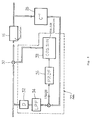
- Fig. 2 is a structural diagram of an embodiment of the present invention.
- Fig. 2 10 is an automatic equaliser (AEQ), which effects equalised compensation for removing intersymbol interference, included in the received point co-ordinate data obtained by demodulating signal points on the complex plane from the received signal of the transmission line (telephone line).
- AEQ automatic equaliser
- phase jitter interference removing circuit 18 designates a carrier automatic phase control circuit (CAPC), which removes phase error and frequency offset which are line deterioration factors included in an output of the automatic equaliser 10.
- CAPC carrier automatic phase control circuit
- a phase jitter interference removing circuit 18 is newly provided in accordance with the present invention and this phase jitter interference removing circuit 18 is realised by a first fixed equaliser 20. Details of the circuit 18 will be given later.
- phase jitter removing circuit 14 Disposed to follow the phase jitter interference removing circuit 18 is a phase jitter removing circuit 14, which is provided with a phase jitter prediction circuit 22 and second and third fixed equalisers 24, 26. These circuits will be explained later.
- phase jitter interference removing circuit 18 is provided after the CAPC 12 and before the phase jitter removing circuit 14 as shown in Fig. 2. The reason for this will now be explained.
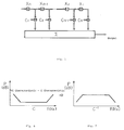
- Fig. 3 indicates the correspondence between cancelling functions on the receiving side and each of the deterioration factors intersymbol interference, phase error/frequency offset, phase jitter interference and phase jitter, these being the major deterioration factors in the transmission line.
- the right hand side of the Figure indicates the necessity for cancelling other deterioration factors before a certain deterioration factor is cancelled.
- phase jitter interference cancellation newly provided by the present invention first to cancel intersymbol interference and phase error/frequency offset, but it does not matter if phase jitter is not first cancelled.
- phase jitter removal first to cancel intersymbol interference, phase error/frequency offset and phase jitter interference.
- phase jitter interference removing circuit 18 of the present invention is located after the CAPC 12 and before the phase jitter removing circuit 14 as shown in Fig. 2.
- phase jitter interference can be removed by supplying an output signal, from which intersymbol interference is removed with the automatic equaliser 10 and phase error and frequency offset are removed with the CAPC 12, to the phase jitter interference removing circuit 18.
- Phase jitter interference depends on the characteristics of the part of the transmission line after an insertion point of the phase jitter.
- a line model shown in Fig. 4 can be used to model the transmission line for the purposes of removing phase jitter interference.
- a typical line model as shown in Fig. 4 can be obtained by considering the above conditions (1) to (3).
- X indicates a transmitted signal, which becomes a signal R under the influence of line characteristic D, 1 becomes a signal K due to the influence of phase jitter exp(j ⁇ ) at the phase jitter inserting point 28, and then becomes an equalised output signal Y as a result of line characteristic C.
- phase jitter interference element to be removed by the present invention of the model shown in Fig. 4 will be investigated as follows.
- this signal changes to the K signal due to the influence of deterioration factors by phase jitter exp(j ⁇ ) at the phase jitter inserting point 28.
- the K signal changes to a Y signal due to the influence of deterioration factors by line characteristic C.
- R ⁇ exp(j ⁇ ) - 1 ⁇ ⁇ C in the final term of formula (4) indicates (phase jitter) + (phase jitter interference element); these coupled deterioration factors of phase jitter and phase jitter interference always exist in a line where phase jitter exists.
- phase jitter interference is cancelled on the basis of the results of computations for the phase jitter interference element, using the final term of formula (4).
- phase jitter interference removing circuit 18 As an input of the phase jitter interference removing circuit 18, there is used a signal from which intersymbol interference and phase frequency offset have been eliminated by the automatic equaliser 10 and CAPC 12.
- This output signal includes only the (phase jitter) + (phase jitter interference element) indicated by the second term in the right hand side of the formula (4).
- the phase jitter interference removing circuit 18 comprises a first equaliser 20 in which is set the line equalising characteristic C ⁇ 1 for the line characteristic C of the phase jitter inserting point 28 and successive points shown in Fig. 4.
- Elimination of the phase jitter interference element by the first equaliser 20 also newly generates intersymbol interference,but such intersymbol interference newly generated by the first equaliser 20 may be cancelled, if necessary, by providing an additional equaliser at the stage preceding the decision circuit 16.
- an output from which the phase jitter interference element is removed in the first equaliser 20 is applied to the phase jitter prediction circuit 22 provided in the phase jitter removing circuit 14 in the next stage, and thereby the phase jitter element exp(-j ⁇ ) is computed.
- the output exp(-j ⁇ ) of prediction circuit 22 is applied to the multiplying point 30 to obtain R by removing phase jitter exp(-j ⁇ ) from the output of first equaliser 20.
- a second equaliser 24 is provided in view of the provision of the first equaliser 20 for removing phase jitter interference.
- the line characteristic C which is the inverse characteristic of the line characteristic C ⁇ 1 of the first equaliser 20, is set in the second equaliser 24.
- the output X from the phase jitter removing circuit 14 thus obtained is sent to the decision circuit 16 to decide the most likely signal point by Viterbi decoding, and this deciding point is output as the final receiving point.
- the receiving point is converted, as is well known, into a bit train corresponding to the co-ordinates on the complex plane of the decided point using a bit map circuit (not illustrated).
- a probabilistic decision error from the decision circuit 16 is fed back, after normalisation, to the phase jitter prediction circuit 22 provided in the phase jitter removing circuit 14, and the normalised output of decision circuit 16 receives equalised compensation by a third equaliser 26 provided in the feedback loop. That is, a line equalising characteristic C which is the same as that of the first equaliser 20 for removing phase jitter interference is set in the third equaliser 26.
- the prediction circuit 22 can be optimised by obtaining the output R by conducting equalised compensation based on the line equalising characteristic C ⁇ 1 upon the normalised output from the decision circuit 16, and then feeding back such output R to the prediction circuit 22.
- a transversal type fixed equaliser is used as the first, second and third equalisers 20, 24, 26 and fixed constants are set, from an experimental viewpoint, as the counting numbers C1 to Cn of the fixed equalisers.
- this unconditioned characteristic of Fig. 6 is considered as the line characteristic C ⁇ 1 of the phase jitter inserting point 28 and the successive points shown in Fig. 4.
- the coefficients C1 to Cn of the transversal type fixed equalisers shown in Fig. 5 are set in the first equaliser 20 and third equaliser 26 so that the inverse characteristic C ⁇ 1 of the unconditioned characteristic of Fig. 6 shown in Fig. 7 can be obtained. Meanwhile, the coefficients C1 to Cn of the fixed equalisers of Fig. 5 are set in the second equaliser 24 of Fig. 2 so that the unconditioned characteristic of Fig. 6 can be obtained.
- the line equalising characteristics C ⁇ 1, C to be set in the equalisers 20, 24, 26 of Fig. 2 are not limited just to the unconditioned characteristic, and an equalising characteristic based on other adequate typical line characteristics can be set instead.
- Fig. 8 indicates a practical structure of an embodiment of the phase jitter prediction circuit 22 provided in the phase jitter removing circuit 14.
- phase jitter prediction circuit 22 shown in Fig. 8
- an output from the first equaliser 20 shown in Fig. 2 is multiplied by the normalised output which is equalised and compensated by the third equaliser through a delay circuit 32 and a low-pass filter 34, and thereafter supplied to the prediction filter 36 after conversion into a scalar value in order to predict the phase jitter element.
- the output of prediction filter 36 is converted back to vector data by a cos/sin converter 38, and multiplied at the multiplying point 30 to remove the phase jitter element.
- a delay circuit 32 shown in Fig. 8 is necessary in the case where the decision circuit 16 makes a probabilistic decision through Viterbi decoding, but is unnecessary for non-probabilistic decision in the decision circuit 16, namely for deciding the nearest signal point on the complex plane for the demodulation receiving point without using a transition rule by trellis encoding in the transmitting side.
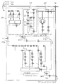
- Fig. 9 is a diagram of the entire structure of an embodiment of the present invention.
- reference numeral 10 designates an automatic equaliser (AEQ) which receives as input co-ordinate data of the receiving point demodulated from the received signal of the transmission line, i.e. the receiving point vector data or pass band signal, and provides an equalised output which is compensated for intersymbol interference in the input vector data.
- AEQ automatic equaliser
- a carrier phase controller 12a is provided following the automatic equaliser 10.
- This carrier phase controller 12a includes a carrier automatic phase control circuit 120 which computes a frequency offset and phase error element included in the equalised output of automatic equaliser 10, and these elements are removed from the equalised output by applying them to a multiplying circuit 121.
- This carrier phase controller 12a is already disclosed by the drawings of specifications, for example, of Japanese Published Patent Application No. 55-33203 or U.S. Patent No. 4,097,807.
- the carrier automatic phase control circuit 120 is known as a secondary CAPC circuit because it is provided following the automatic equaliser 10.
- phase jitter interference remover 18 described previously is provided to remove and suppress the elements, other than the true phase jitter element in the line, from whatever phase jitter is not removed perfectly in the carrier phase controller 12a.
- phase jitter removing means 14 is provided. This removes the phase jitter element from an output, in which the phase jitter element is amplified, of the phase jitter interference remover 18.
- a decision circuit 16 is provided.
- the decision circuit 16 is provided with a probabilistic or non-probabilistic decision circuit 160, which decides, in the case of a probabilistic decision, the most likely signal point on the complex plane and corrects an error in the receiving signal point by utilising a degree of redundancy added at the transmitting side. That is, since a redundant bit is added for controlling errors by a trellis encoding circuit provided in the data modem in the transmitting side, the most likely signal point is decided by Viterbi decoding utilising single redundant bits added by trellis encoding. On the other hand, in the case of a non-probabilistic decision, the decision is made directly by using a table.
- the receiving decision point determined by the probabilistic or non-probabilistic decision circuit 160 is given to a co-ordinates/bit train converting circuit (not illustrated) provided in the successive stage, and is then converted to the bit train corresponding to the signal points.
- the decided output of the decision circuit 160 is applied to one input of an adder 162, and an input to the decision circuit 160 is applied through a delay circuit 161 to the other input of adder 162, in order to extract a difference between the decision point and the receiving point obtained through the delay circuit 161, namely the probabilistic or non-probabilistic decision error.
- the decision error obtained from the adder 162 is fed back to the phase jitter remover 14 and is then used for optimisation of a prediction filter as explained later.
- the time constants of controller 12a are set larger for this purpose.
- a degree of feedback to the multiplier 121 in the CAPC 120 of Fig. 9 is set to smaller value. As a result, the trackability of low speed jitter (low frequency jitter) by the carrier automatic phase control circuit is lowered and the carrier phase controller 12a can no longer sufficiently remove low frequency jitter.
- the low frequency jitter which is not sufficiently removed by the carrier phase controller 12a has to be removed by the phase jitter remover 14 in the next and successive stages; however, the prediction filter 22 provided in the phase jitter remover 14 has very weak trackability for low frequency because a number of taps thereof is finite. Accordingly, even when the prediction filter 22 of phase jitter remover 14 is operated directly, it cannot follow low frequency jitter and therefore cannot remove phase jitter sufficiently.
- phase jitter remover 14 is explained in detail as follows.
- the receiving point data namely receiving point vector data from which the intersymbol interference, frequency offset and phase error have been removed by the automatic equaliser 10 and carrier phase controller 12a
- the delay circuit 141 is multiplied with a normalised signal NOR in the multiplier 142.
- the vector elements namely the co-ordinate value R on the real number axis and the co-ordinate value I on the imaginary number axis in the complex plane based on the input vector data, are generated by the Hilbert filters 143-1, 143-2.
- the vector elements R, I generated by the Hilbert filters 143-1, 143-2, are input to the prediction filter 22 after frequency-modulation by frequency fc in the modulation circuit 140a. That is, the frequency is shifted to the right (increased) by +fc.
- the vector elements R, I indicating computed phase jitter elements, are applied to the demodulation circuit 140b provided in the output stage, where they are returned to the original frequency through demodulation by frequency fc, then applied to the multiplier 30 after conversion back to vector data by the ⁇ - sin ⁇ , cos ⁇ conversion circuit 144.
- the phase jitter element included in the output given via the carrier phase controller 12 and phase jitter interference remover 18 is removed.
- the probabilistic or non-probabilistic decision error from the adder 162 provided in the decision part 16 is normalised by NOR (normalised data) of a multiplier 145, given to the third equaliser 26 as explained previously, and thereafter converted to the vector elements R, I, by the Hilbert filters 146-1, 146-2.
- This error signal as a normalised vector element is applied to the modulation circuit 140c and is frequency-modulated by the frequency fc as in the case of modulation circuit 140a, and thereafter applied as the error signal for optimising the prediction filter 22.
- the operation frequency region of prediction filter 22 is changed, by the modulation circuits 140a, 140c and demodulation circuit 140b provided at the input/output ends of prediction filter 22, to a higher frequency operation region in which the frequency is shifted by the modulation frequency fc.
- This frequency shift of the operation region allows the prediction filters 14-2, which provide only weak tracking at lower frequencies, to follow lower frequency jitter satisfactorily.
- low frequency jitter which has not yet been removed by the carrier phase controller 12a is also predicted accurately by the prediction filter 22 and can be removed by the multiplier 30.
- the automatic equaliser 10, carrier phase controller 12a, phase jitter interference remover 18, phase jitter remover 14 and decision circuit 16 shown in Fig. 9 can be implemented using a digital signal processor (DSP).
- DSP digital signal processor
- Fig. 10 is a structural diagram of an embodiment indicating the algorithm, realised by a DSP, of the phase jitter prediction circuit 22 of Fig. 8 provided in the phase jitter removing circuit 14.
- T indicates a tap register; ⁇ , multiplication; ⁇ , addition and ⁇ , summing (totalisation).
- the arrow mark without any coefficient code denotes a constant value.
- a vector input and a scalar input are given to the phase jitter prediction circuit.
- the scalar input is given to the prediction filter 22 through a low-pass filter 34.
- the normalised vector input is applied, after equalisation with the line equalising characteristic C ⁇ 1 to the prediction filter 22.
- a predicted signal of the prediction filter 22 is frequency-shifted by the demodulating computation 140b, then converted into vector data by the cos/sin converting circuit 144, normalised in its amplitude in the amplitude normalising circuit 144′, and is then input to the multiplying point 30 to cancel the phase jitter element included in the vector input.
- the present invention is capable of substantially removing deterioration factors of a transmission line by removing phase jitter interference generated in the line after the phase jitter factor inserting point, and is capable of realising high-quality data transmission for a super-high-speed modem by improving the S/N error rate and also extending the application range.
- a next-stage prediction filter which was previously inferior in tracking at lower frequencies can be made to follow low-frequency jitter satisfactorily, by operating the filter in a shifted frequency operation region.
- Low-frequency jitter left through the carrier phase control by feedback of probabilistic or non-probabilistic decision error can also be suppressed and removed by effectively utilising the prediction filter.
Landscapes
- Engineering & Computer Science (AREA)
- Computer Networks & Wireless Communication (AREA)
- Signal Processing (AREA)
- Quality & Reliability (AREA)
- Cable Transmission Systems, Equalization Of Radio And Reduction Of Echo (AREA)
- Digital Transmission Methods That Use Modulated Carrier Waves (AREA)
- Dc Digital Transmission (AREA)
Abstract
Claims (6)
- Système d'élimination de détérioration de signaux de ligne comprenant :
un égaliseur automatique (10) pour éliminer une interférence entre symboles d'un signal reçu sur une ligne de transmission ;
un dispositif d'élimination d'instabilité de phase (14) pour éliminer un élément d'instabilité de phase compris dans le signal reçu ;
un dispositif de décision (16) qui est placé après au moins ledit égaliseur automatique (10) et un dispositif d'élimination d'instabilité de phase (14) pour contribuer à l'élimination de l'interférence entre symboles et de l'instabilité de phase dans le signal reçu en décidant du point de signal de vraisemblance maximum ; caractérisé en ce que :
un dispositif d'élimination d'interférence d'instabilité de phase (18) est prévu pour compenser une interférence d'instabilité de phase entre des instabilités de phase générées lorsque ledit élément d'instabilité de phase est appliqué audit égaliseur automatique (10), ledit dispositif de décision (16) étant placé après ledit dispositif d'élimination d'interférence d'instabilité de phase (18) et en utilisant le signal à partir duquel l'interférence d'instabilité de phase est éliminée. - Système d'élimination de détérioration de signal de ligne selon la revendication 1, dans lequel ledit dispositif d'élimination d'interférence d'instabilité de phase (18) comprend un premier égaliseur (20) ayant une caractéristique d'égalisation de ligne pour un point d'insertion d'instabilité de phase (28) et des points successifs sur la ligne de transmission, pour éliminer une interférence d'instabilité de phase comprise dans le signal d'entrée fourni audit dispositif d'élimination d'interférence d'instabilité de phase (18).
- Système d'élimination de détérioration de signal de ligne selon la revendication 1 ou 2, dans lequel ledit dispositif d'élimination d'instabilité de phase (14) comprend un second égaliseur (24) ayant la caractéristique de ligne inverse à celle dudit premier égaliseur (20), de sorte qu'un signal sans ledit élément d'instabilité de phase est fourni audit dispositif de décision (16) après égalisation par ledit second égaliseur (24).
- Système d'élimination de détérioration de signal de ligne selon la revendication 2 ou 3, dans lequel ledit dispositif d'élimination instabilité de phase (14) comprend en outre un troisième égaliseur (26) ayant une caractéristique d'égalisation de ligne identique à celle dudit premier égaliseur (20), de sorte que ledit troisième égaliseur réalise une égalisation sur la sortie normalisée dudit dispositif de décision (16) et renvoie ensuite le signal égalisé pour une optimisation dudit dispositif d'élimination d'instabilité de phase (14).
- Système d'élimination de détérioration de signal de ligne selon la revendication 2, 3, et 4, dans lequel un égaliseur fixe du type à filtre transversal est utilisé comme lesdits premier, second, et troisième égaliseurs (20, 24, 26).
- Système d'élimination de détérioration de signal de ligne selon l'une quelconque des revendications précédentes, dans lequel un dispositif d'égalisation pour éliminer une interférence entre symboles générée pendant l'élimination de l'interférence d'instabilité de phase par ledit dispositif d'élimination d'élément d'interférence d'instabilité de phase (18) est fourni additionnellement à un étage précédent ledit dispositif de décision (16).
Priority Applications (1)
| Application Number | Priority Date | Filing Date | Title |
|---|---|---|---|
| EP94106754A EP0621712B1 (fr) | 1989-06-13 | 1990-06-06 | Annulateur de distortion pour récepteur de ligne |
Applications Claiming Priority (5)
| Application Number | Priority Date | Filing Date | Title |
|---|---|---|---|
| JP151274/89 | 1989-06-13 | ||
| JP15127389A JP2965999B2 (ja) | 1989-06-13 | 1989-06-13 | データモデム |
| JP1151274A JP2966000B2 (ja) | 1989-06-13 | 1989-06-13 | データモデム |
| JP151273/89 | 1989-06-13 | ||
| PCT/JP1990/000735 WO1990016117A1 (fr) | 1989-06-13 | 1990-06-06 | Systeme d'elimination des deteriorations de signaux de circuits |
Related Child Applications (2)
| Application Number | Title | Priority Date | Filing Date |
|---|---|---|---|
| EP94106754A Division EP0621712B1 (fr) | 1989-06-13 | 1990-06-06 | Annulateur de distortion pour récepteur de ligne |
| EP94106754.8 Division-Into | 1994-04-29 |
Publications (3)
| Publication Number | Publication Date |
|---|---|
| EP0433458A1 EP0433458A1 (fr) | 1991-06-26 |
| EP0433458A4 EP0433458A4 (en) | 1991-11-21 |
| EP0433458B1 true EP0433458B1 (fr) | 1995-03-29 |
Family
ID=26480575
Family Applications (2)
| Application Number | Title | Priority Date | Filing Date |
|---|---|---|---|
| EP94106754A Expired - Lifetime EP0621712B1 (fr) | 1989-06-13 | 1990-06-06 | Annulateur de distortion pour récepteur de ligne |
| EP90908639A Expired - Lifetime EP0433458B1 (fr) | 1989-06-13 | 1990-06-06 | Systeme d'elimination des deteriorations de signaux de circuits |
Family Applications Before (1)
| Application Number | Title | Priority Date | Filing Date |
|---|---|---|---|
| EP94106754A Expired - Lifetime EP0621712B1 (fr) | 1989-06-13 | 1990-06-06 | Annulateur de distortion pour récepteur de ligne |
Country Status (5)
| Country | Link |
|---|---|
| US (1) | US5189684A (fr) |
| EP (2) | EP0621712B1 (fr) |
| CA (1) | CA2028820C (fr) |
| DE (1) | DE69018211T2 (fr) |
| WO (1) | WO1990016117A1 (fr) |
Families Citing this family (6)
| Publication number | Priority date | Publication date | Assignee | Title |
|---|---|---|---|---|
| JPH08172464A (ja) * | 1994-12-20 | 1996-07-02 | Fujitsu Ltd | キャリア位相制御回路 |
| JP3351642B2 (ja) * | 1994-12-20 | 2002-12-03 | 富士通株式会社 | 位相ジッタ抽出回路及び位相ジッタキャンセル回路 |
| JP3396318B2 (ja) * | 1994-12-20 | 2003-04-14 | 富士通株式会社 | 自動等化器 |
| US7577192B2 (en) * | 2001-03-29 | 2009-08-18 | Applied Wave Research, Inc. | Method and apparatus for characterizing the distortion produced by electronic equipment |
| TWI452880B (zh) * | 2009-09-03 | 2014-09-11 | Realtek Semiconductor Corp | 等化裝置 |
| US11239991B2 (en) * | 2020-04-28 | 2022-02-01 | Marvell Asia Pte, Ltd. | Systems and methods for timing recovery with bandwidth extension |
Family Cites Families (10)
| Publication number | Priority date | Publication date | Assignee | Title |
|---|---|---|---|---|
| US3727134A (en) * | 1971-03-29 | 1973-04-10 | Collins Radio Co | Auto equalizer apparatus |
| US3887874A (en) * | 1974-05-10 | 1975-06-03 | Rockwell International Corp | Low pass filter apparatus |
| US3962637A (en) * | 1974-11-11 | 1976-06-08 | Hycom Incorporated | Ultrafast adaptive digital modem |
| JPS5182548A (en) | 1974-12-27 | 1976-07-20 | Fujitsu Ltd | Jidotokaki |
| JPS5533203A (en) | 1978-08-30 | 1980-03-08 | Hitachi Ltd | Graphic generator of raster-scanning type display unit |
| JPS59105741A (ja) * | 1982-12-09 | 1984-06-19 | Nec Corp | 8相位相復調器 |
| JPS5962228A (ja) * | 1982-10-01 | 1984-04-09 | Nec Corp | 自動等化器 |
| US4669096A (en) * | 1984-09-17 | 1987-05-26 | Heimbuch William G | Differential data line selector |
| JPS6211326A (ja) * | 1985-07-09 | 1987-01-20 | Hitachi Ltd | 自動等化器再設定方式 |
| NL8700125A (nl) * | 1987-01-20 | 1988-08-16 | Philips Nv | Inrichting voor het bestrijden van intersymboolinterferentie en ruis. |
-
1990
- 1990-06-06 DE DE69018211T patent/DE69018211T2/de not_active Expired - Fee Related
- 1990-06-06 WO PCT/JP1990/000735 patent/WO1990016117A1/fr active IP Right Grant
- 1990-06-06 EP EP94106754A patent/EP0621712B1/fr not_active Expired - Lifetime
- 1990-06-06 US US07/582,207 patent/US5189684A/en not_active Expired - Lifetime
- 1990-06-06 EP EP90908639A patent/EP0433458B1/fr not_active Expired - Lifetime
- 1990-06-06 CA CA002028820A patent/CA2028820C/fr not_active Expired - Fee Related
Also Published As
| Publication number | Publication date |
|---|---|
| CA2028820C (fr) | 1995-06-13 |
| US5189684A (en) | 1993-02-23 |
| EP0621712A2 (fr) | 1994-10-26 |
| EP0433458A1 (fr) | 1991-06-26 |
| CA2028820A1 (fr) | 1990-12-14 |
| WO1990016117A1 (fr) | 1990-12-27 |
| DE69018211D1 (de) | 1995-05-04 |
| EP0621712B1 (fr) | 2001-03-07 |
| EP0621712A3 (fr) | 1994-12-07 |
| DE69018211T2 (de) | 1995-07-27 |
| EP0433458A4 (en) | 1991-11-21 |
Similar Documents
| Publication | Publication Date | Title |
|---|---|---|
| EP0684708B1 (fr) | Egaliseur a adaptation automatique | |
| US5465276A (en) | Method of forming a channel estimate for a time-varying radio channel | |
| EP0601855A2 (fr) | Egaliseur adaptatif, capable de compenser un décalage de la fréquence porteuse | |
| EP0366160A1 (fr) | Analyseur non intrusif des distorsions introduites par le canal de transmission | |
| EP1168744A1 (fr) | Dispositif de reproduction de temporisation et demodulateur | |
| US6628926B1 (en) | Method for automatic frequency control | |
| US7016404B2 (en) | Automatic frequency correction for mobile radio receivers | |
| JP3237827B2 (ja) | 無線データ通信端末 | |
| EP0453814B1 (fr) | Système adaptatif d'estimation de réponses impulsionnelles de canal au moyen d'estimation de séquence ayant un maximum de vraisemblance | |
| EP0692895A2 (fr) | Démodulateur utilisant une détection différentielle | |
| JPH03133218A (ja) | ディジタル信号受信方式及び受信装置 | |
| EP0433458B1 (fr) | Systeme d'elimination des deteriorations de signaux de circuits | |
| JP3160453B2 (ja) | データ受信装置 | |
| US5517526A (en) | Timing recovery device in a receiver circuit for modems | |
| US4330861A (en) | Digital equalizer for signal receiver in QPSK data-transmission system | |
| US7315587B2 (en) | Demodulation method and apparatus based on differential detection system for π/4 shifted QPSK modulated wave | |
| JP4315549B2 (ja) | 信号キャリア回復処理方法 | |
| TWI237452B (en) | Reducing phase noise in phase-encoded communications signals | |
| JP3851143B2 (ja) | 変調方式識別回路、これを備えた受信装置、無線局、及び変調方式識別方法 | |
| EP1060601B1 (fr) | Demodulateur a dispositif de rotation pour correction de decalage de frequence | |
| JP2965999B2 (ja) | データモデム | |
| US5926511A (en) | Process for the coherent demodulation of a reception signal | |
| US20010019582A1 (en) | Frequency modulation method and modem unit employing such method | |
| KR100524934B1 (ko) | 버스트 모드 수신기를 위한 프레임 동기 장치 및 그 방법 | |
| JPH0951295A (ja) | データ受信装置 |
Legal Events
| Date | Code | Title | Description |
|---|---|---|---|
| PUAI | Public reference made under article 153(3) epc to a published international application that has entered the european phase |
Free format text: ORIGINAL CODE: 0009012 |
|
| 17P | Request for examination filed |
Effective date: 19901221 |
|
| AK | Designated contracting states |
Kind code of ref document: A1 Designated state(s): DE FR GB |
|
| A4 | Supplementary search report drawn up and despatched |
Effective date: 19910927 |
|
| AK | Designated contracting states |
Kind code of ref document: A4 Designated state(s): DE FR GB |
|
| 17Q | First examination report despatched |
Effective date: 19931112 |
|
| GRAA | (expected) grant |
Free format text: ORIGINAL CODE: 0009210 |
|
| AK | Designated contracting states |
Kind code of ref document: B1 Designated state(s): DE FR GB |
|
| XX | Miscellaneous (additional remarks) |
Free format text: TEILANMELDUNG 94106754.8 EINGEREICHT AM 06/06/90. |
|
| REF | Corresponds to: |
Ref document number: 69018211 Country of ref document: DE Date of ref document: 19950504 |
|
| ET | Fr: translation filed | ||
| PLBE | No opposition filed within time limit |
Free format text: ORIGINAL CODE: 0009261 |
|
| STAA | Information on the status of an ep patent application or granted ep patent |
Free format text: STATUS: NO OPPOSITION FILED WITHIN TIME LIMIT |
|
| 26N | No opposition filed | ||
| REG | Reference to a national code |
Ref country code: GB Ref legal event code: IF02 |
|
| PGFP | Annual fee paid to national office [announced via postgrant information from national office to epo] |
Ref country code: GB Payment date: 20050601 Year of fee payment: 16 |
|
| PGFP | Annual fee paid to national office [announced via postgrant information from national office to epo] |
Ref country code: DE Payment date: 20050602 Year of fee payment: 16 |
|
| PGFP | Annual fee paid to national office [announced via postgrant information from national office to epo] |
Ref country code: FR Payment date: 20050608 Year of fee payment: 16 |
|
| PG25 | Lapsed in a contracting state [announced via postgrant information from national office to epo] |
Ref country code: GB Free format text: LAPSE BECAUSE OF NON-PAYMENT OF DUE FEES Effective date: 20060606 |
|
| PG25 | Lapsed in a contracting state [announced via postgrant information from national office to epo] |
Ref country code: DE Free format text: LAPSE BECAUSE OF NON-PAYMENT OF DUE FEES Effective date: 20070103 |
|
| GBPC | Gb: european patent ceased through non-payment of renewal fee |
Effective date: 20060606 |
|
| REG | Reference to a national code |
Ref country code: FR Ref legal event code: ST Effective date: 20070228 |
|
| PG25 | Lapsed in a contracting state [announced via postgrant information from national office to epo] |
Ref country code: FR Free format text: LAPSE BECAUSE OF NON-PAYMENT OF DUE FEES Effective date: 20060630 |