EP0433458A1 - Systeme d'elimination des deteriorations de signaux de circuits - Google Patents
Systeme d'elimination des deteriorations de signaux de circuits Download PDFInfo
- Publication number
- EP0433458A1 EP0433458A1 EP90908639A EP90908639A EP0433458A1 EP 0433458 A1 EP0433458 A1 EP 0433458A1 EP 90908639 A EP90908639 A EP 90908639A EP 90908639 A EP90908639 A EP 90908639A EP 0433458 A1 EP0433458 A1 EP 0433458A1
- Authority
- EP
- European Patent Office
- Prior art keywords
- phase jitter
- phase
- equalizer
- signal
- jitter
- Prior art date
- Legal status (The legal status is an assumption and is not a legal conclusion. Google has not performed a legal analysis and makes no representation as to the accuracy of the status listed.)
- Granted
Links
- 230000006866 deterioration Effects 0.000 title claims abstract description 34
- 230000005540 biological transmission Effects 0.000 claims description 26
- 238000005457 optimization Methods 0.000 claims description 4
- 238000010606 normalization Methods 0.000 claims description 3
- 238000007476 Maximum Likelihood Methods 0.000 claims description 2
- 238000010586 diagram Methods 0.000 description 11
- 238000000034 method Methods 0.000 description 7
- 238000006243 chemical reaction Methods 0.000 description 3
- 238000003780 insertion Methods 0.000 description 2
- 230000037431 insertion Effects 0.000 description 2
- 238000012545 processing Methods 0.000 description 2
- 230000000694 effects Effects 0.000 description 1
- 230000008030 elimination Effects 0.000 description 1
- 238000003379 elimination reaction Methods 0.000 description 1
- 238000011156 evaluation Methods 0.000 description 1
- 239000000284 extract Substances 0.000 description 1
- 230000006872 improvement Effects 0.000 description 1
- 238000011835 investigation Methods 0.000 description 1
- 230000008569 process Effects 0.000 description 1
- 230000004044 response Effects 0.000 description 1
- 230000007480 spreading Effects 0.000 description 1
- 230000007704 transition Effects 0.000 description 1
Images


Classifications
-
- H—ELECTRICITY
- H04—ELECTRIC COMMUNICATION TECHNIQUE
- H04L—TRANSMISSION OF DIGITAL INFORMATION, e.g. TELEGRAPHIC COMMUNICATION
- H04L27/00—Modulated-carrier systems
- H04L27/18—Phase-modulated carrier systems, i.e. using phase-shift keying
- H04L27/22—Demodulator circuits; Receiver circuits
- H04L27/233—Demodulator circuits; Receiver circuits using non-coherent demodulation
- H04L27/2332—Demodulator circuits; Receiver circuits using non-coherent demodulation using a non-coherent carrier
-
- H—ELECTRICITY
- H04—ELECTRIC COMMUNICATION TECHNIQUE
- H04L—TRANSMISSION OF DIGITAL INFORMATION, e.g. TELEGRAPHIC COMMUNICATION
- H04L1/00—Arrangements for detecting or preventing errors in the information received
- H04L1/20—Arrangements for detecting or preventing errors in the information received using signal quality detector
- H04L1/205—Arrangements for detecting or preventing errors in the information received using signal quality detector jitter monitoring
-
- H—ELECTRICITY
- H04—ELECTRIC COMMUNICATION TECHNIQUE
- H04L—TRANSMISSION OF DIGITAL INFORMATION, e.g. TELEGRAPHIC COMMUNICATION
- H04L27/00—Modulated-carrier systems
- H04L27/0014—Carrier regulation
- H04L2027/0024—Carrier regulation at the receiver end
- H04L2027/0026—Correction of carrier offset
- H04L2027/003—Correction of carrier offset at baseband only
-
- H—ELECTRICITY
- H04—ELECTRIC COMMUNICATION TECHNIQUE
- H04L—TRANSMISSION OF DIGITAL INFORMATION, e.g. TELEGRAPHIC COMMUNICATION
- H04L27/00—Modulated-carrier systems
- H04L27/0014—Carrier regulation
- H04L2027/0044—Control loops for carrier regulation
- H04L2027/0053—Closed loops
- H04L2027/0057—Closed loops quadrature phase
Definitions
- the present invention relates to a data modem for detecting and cancelling line deterioration factor and particularly to a line signal deterioration removing system to be employed for data modem which effectively removes phase jitter factor.
- the data transmission utilizing the telephone line having the transmission band in the voice frequency range is recently spreading.
- a so-called modem usually providing a modulator in the sending side and a demodulator in the receiving side is provided and various line deterioration factors generated in the line between the modems are removed by such modems provided in the sending side and receiving side.
- the recent modulation system since the recent modulation system has improved the data transmission rate through introduction of multiphase modulation system, it is requested to equalize, with high accuracy, various kinds of signal deteriorations in relation to the phases of the signals to be transmitted such as intersymbol interferences effectuated on the line, frequency offset generated due to difference of carrier frequencies for modulation and demodulation and phase jitter generated due to fluctuation of power source voltage.
- Fig. 11 is a structural diagram of algorithm within the modem of receiving side of the prior art. Such structure is executed by programs using digital signal processing LSIs and microprocessors.
- reference numeral 10 designates an automatic equalizer (AEQ) which is for exmaple formed by a transversal filter.
- AEQ automatic equalizer
- the base band signal after the demodulation or the pass band signal before demodulation which is received from the transmission line is input as the coordinates data (vector data) of signal points on the complex plane.
- vector data vector data
- the equalized output obtained by removing the intersymbol interference element as the line deterioration factor 1 from such input signal is thus output.
- CAPC 12 foresees frequency offset and phase error included in the equalized output of equalizer 10 with the integral operation of quadratic form.
- An output of CAPC is multiplied, in vector, respectively with the equalized output of equalizer 10 and feedback signal to the equalizer at the position where the conjugate vector * is indicated by the symbol x of multiplication
- Multiplication to output of automatic equalizer 10 means stop of phase rotation, namely demodulation and multiplicaiton, on the contrary, to feedback signal to the automatic equalizer 10 means addition of phase rotation, namely modulation.
- the principle of removing carrier frequency offset with such structure is based on the principle that the phase of output of automatic equalizer 10 rotates at a constant angular velocity due to the influence of carrier frequency offset but this rotation can be ceased by multiplying an output of CAPC 12.
- a hard non-probablistic decision error given as phase difference between the non-probablistic decision point and receiving point by a non-probablistic decision circuit 26 is input.
- CAPC 12 computes frequency offset and phase error element included in the output of equalizer 12 based on such hard decision error. The computation result is multiplied to the equalizer output.
- This structure is known as the non-probablistic decision error feedback system because the non-probablistic decision error obtained from the decision output of the non-probablistic decision circuit 26.
- phase jitter remover including a prediction filter circuit 14 is provided.
- the prediction filter circuit 14 predicts phase jitter element with a comprised prediction filter. An output thereof is multiplied to an output value of the carrier phase controller at the part of multiplication code in order to remove phase jitter element from output of the carrier phase controller.
- Respective line deterioration factors such as intersymbol inteference, frequency offset, phase error and phase jitter are removed and the revmoed receiving point information is finally applied to a soft (probablistic) decision circuit or non-probablistic decision circuit 16.
- the probablistic decision circuit decides, based on the input value, the most likelihood signal point which the receiving signal takes by the well known viterbi decoding.
- the signal points assigned corresponding to the regions assigned to each complex space are decided using the tables corresponding to the values of respective regions.
- Decision error given as an error between the decision point of the probablistic decision circuit or non-probablistic decision circuit 16 is fed back to the prediction filter circuit 14 as a normalized output for optimization control of the prediction filter circuit 14. Moreover, this error is also fed back to the automatic equalizer 10 through a couple of multiplizers.
- intersymbol interference which is a signal deterioration factor of transmission line is removed by the automatic equalizer 10, while frequency offset and phase error by the carrier phase controller and phae jitter by phase jitter remover.
- the conventional modem does not require very highly accurate demodulation and compensation for phase because the transmission rate is low, but when it is applied to demodulation of high transmission rate, the signal deterioration factors cannot be removed perfectly, resulting in a problem that phase error becomes numerous.
- the conventional structure explained above is preferable in such a point that high trackability for distortion of phase error can be obtained by using a non-probablistic decision circuit which can suppress delay within the loop to zero for the control of CAPC 12 by feedback of non-probablistic decision error.
- It is another object of the present invention to provide a line signal deterioration compensating apparatus comprising an automatic equalizer, namely a method and an apparatus for decising signals with high accuracy after removing phase jitter interference through preceding equalization by automatic equalizer.
- the inventors of the present invention have found as a result of analysis for the uncompensated element that an automatic equalizer is formed by a transversal type filter, each signal is shifted on tap from the past to the future in order to compensate for intersymbol interference and the phase jitter element included in the one of a plurality of receiving signals is partly uncompensated because such element gives influence on the output signal while it exists on on the taps.
- phase jitter can certainly be compensated by removing or suppressing influence on the phase jitter during compensation for intersymbol interference with predetermined removing circuit before removing phase jitter using a prediction filter.
- response time constant of CAPC is set to a large value in order to stabilize operations of CAPC.
- the trackability for phase jitter of lower frequency may be lowered.
- This phase jitter is removed by predicting it with the prediction filter.
- the prediction filter is formed by a transversl type filter providing a limited number of taps for shifting signals, it shows remarkably low trackability for lower frequency.
- a frequency shift means for multiplying predetermined frequency to the input signal of operation frequency of the prediction filter is provided in the preceding stage of the prediction filter. Thereby, the prediction filter can process the high frequency signal and has the sufficient removing capability to low frequency phase jitter.
- Fig. 1 is a diagram for explaining the principle of the present invention.
- Fig. 2 is a structure indicating the principle of a preferred embodiment of the present invention.
- Fig. 3 is a diagram for explaining allocating condition of phase jitter interference cancelling function of the present invention.
- Fig. 4 is a line model in the present invention.
- Fig. 5 is a structural diagram of an embodiment of a fixed equalizer to be used in the present invention.
- Fig. 6 and Fig. 7 are diagrams for explaining unconditioned line characteristic and equalizing characteristic.
- Fig. 8 is a structural diagram of an embodiment of phase jitter prediction circuit of the present invention.
- Fig. 9 is an entire structural diagram of an embodiment of the present invention.
- Fig. 10 is an algorithm diagram of detail embodiment of the essential portion of the present invention realized with a digital signal processor.
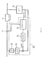
- an automatic equalizing means 10 removes intersymbol interference element from the signal point information on the complex plane or pass band signal demodulated from the receiving signal of transmission line.
- a carrier automatic phase control means 12 removes phase error and frequency offset element included in the equalized output of the automatic equalizing means 10.
- a phase jitter removing means 14 removes phase jitter element included in the output of the carrier automatic phase control means 12.
- a deciding means 16 decides a signal point on the most liklihood complex plane, in the case of the probablistic decision, utilizing redundancey added in the sending side, based on an output of the phase jitter removing means 14, moreover decides in direct in the case of the non-probablistic decision and generates an error between the ideal receiving point and the actual receiving point.
- phase jitter interference removing means 18 is additionally disposed in the successive stage of the automatic equalizing means 10 and CAPC 12.
- a modulating means and a demodulating means are provided before and after the phase jitter prediction filter to be provided to the phase jitter removing means 14 and moreover a modulating means is provided for the feedback signal to the prediction filter.
- a phase jitter interference removing means 18 receives phase jitter influenced by compensation for intersymbol interference and frequency offset in the automatic equalizing means 10 and CAPC 12.
- the phase jitter interference removing means 18 filters such receiving signals with a filter having the characteristic approximated to the line characteristic such as a fixted filter and amplifies and extracts only the transmitting signal and phse jitter as the outputs.
- phase jitter interference removing means 18 An output of the phase jitter interference removing means 18 is supplied to the phase jitter removing means 14.
- This phase jitter removing means 14 removes the amplified phase jitter and phase jitter element from the combined signal of transmitting signals and then supplies the phase jitter free signal to the deciding means 16.
- the phase jitter removing means 14 is capable of processing a low frequency phase jitter at a higher frequency since it can raise the input signal frequency up to the determined frequency, namely, is capable of improving S/N characteristic because phase jitter becomes a signal to be processed easily on the frequency axis.
- Fig. 2 is a structural diagram of an embodiment of the present invention.
- reference numeral 10 designates an automatic equalizer (AEQ), which conducts equalized compensation for removing intersymbol interference included in the receiving point coordinates data obtained by demodulating signal points on the complex plane from the receiving signal of the transmission line (telephone line).
- AEQ automatic equalizer
- Referecne numeral 12 designates a carrier automatic phase control circuit (CAPC), which removes phase error and frequency offset which are line deterioration factors included in an output of the automatic equalizer 10.
- a phase jitter interference removing circuit 18 is newly provided in the present invention and this phase jitter interference removing circuit 18 is realized by a first fixed equalizer 20. Details of such phase jitter interference removing circuit 18 will be made apparent later.
- phase jitter removing circuit 14 is disposed and this phase jitter removing circuit 14 is provided with a phase jitter prediction circuit 22 and first and second fixed equalizers 24, 26. These circuits will then be made apparent later.
- a decision circuit 16 is provided. This decision circuit 16 decides and outputs the most likeligood signal point corresponding to the receiving signal point by the maximum likelihood decoding, namely the viterbi decoding corresponding to addition of redundant one bit due to the trellis encoding conducted for error control in the transmitting side. Moreover, a decision error output (probablistic decision error output) of decision circuit 16 is fed back as a normalized output in order to optimize the phase jitter prediction circuit 22 of the phase jitter removing means.
- the phase jitter interference removing circuit 18 is provided after the carrier automatic phase control circuit 12 and before the phase jitter removing circuit 14 as shown in the embodiment of Fig. 2, which is newly done in the present invention will be explained.
- Fig. 3 indicates correspondence of cancelling function in the receiving side for each of the intersymbol interference, phase error/frequency offset, phase jitter interfence and phase jitter as the major deterioration factors in the transmission line and moreover indicates, in the right side, the necessity for suggesting that the other deterioration factors are already cancelled or not before cancelling a certain deterioration factor.
- phase jitter interference cancel newly provided by the present invention to precedingly cancel intersymbol intererence and phase error/frequency offset and phase jitter, if it is not cancelled, does not result in any problem on the contrary.
- phase jitter removing circuit to cancel phaset jitter to precedingly cancel intersymbol interference, phase error/frequency offset and phase jitter interference.
- phase jitter interference removing circuit 18 of the present invention is provided at the position after the carrier automatic phase control circuit 12 and before the phase jitter removing circuit 14 as shown in Fig. 2, and thereby phase jitter interference element can be removed by giving an output from which intersymbol interference is removed with the automatic equalizer 10 and phase error and frequency offset with the carrier automatic phase control circuit 12 to the phase jitter interference removing circuit 18.
- Phase jitter interference to be removed by the present invention depends on characteristics of transmission line after the factor inserting point of the phase jitter. Therefore, a line model shown in Fig. 4 is considered as the transmission line for removing phase jitter interference of Fig. 2.
- a typical line model as shown in Fig. 4 can be obtained, considering the requirements for determining such line model.
- X indicates a transmitting signal, which becomes R signal by influence of line characteristric D and then becomes K signal by influence of phase jitter exp(j ⁇ ) at the phase jitter inserting point 28 and then becomes equalized output signal Y by influence of line characteristic C.
- phase jitter interference element to be removed by the present invention of the model shown in Fig. 4 will be investigated as follow.
- the transmitting signal X changes to the R signal with influence of deterioration factor by line characteristic D and this R signal is expressed as follow.
- R X ⁇ D (1)
- the K signal changes to Y signal due to influence of deterioration factor by line characteristic C.
- the Y signal is expressed as follow.
- R ⁇ exp (j ⁇ ) - 1 ⁇ C in the last developing term of the formula (4) indicates (phase jitter) + (phase jitter interference element) and a couple deterioration factors of phase jitter and phase jitter interference always exist in the line where phase jitter exists.
- phase jitter inteference is cancelled on the basis of the result of computation for phase jittter interference element indicated by the last developing term of the formula (4).
- phase jitter interference removing circuit 18 As an input of the phase jitter interference removing circuit 18, the outputs having eliminated intersymbol interference and phase frequency offset of the automatic equalizer 10 and carrier automatic phase control circuit 12 are used and this output signal includes only the (phase jitter) + (phase jitter inteference element) indicated by the second term in the right side of the formula (4).
- the phase jitter interference removing circuit 18 comprises a first equalizer 20 which has set the line equalizing characteristic C ⁇ 1 for the line characteristic C of the phase jitter inserting point 28 and successive points shown in Fig. 4 to eliminate phase jitter interference element by effectuating equalizing compensation by the line equalizing characteristic C ⁇ 1 to the output of carrier automatic phase control circuit 12. Namely, since an output of the carrier automatic phase control circuit 12 is expressed as X + R (exp (j ⁇ ) - 1) C, R x exp (j ⁇ ) including only the phase jitter element having removed phase jitter interference element can be obtained by conducting equalized compensation based on the line equalizing characteristic C ⁇ 1 to such output.
- Elimination of phase jitter interference element by the first equalier 20 also newly generates intersymbol interference but such intersymbol interference newly generated by the first equalizer 20 may be cancelled, if necessary, by additionally providing an equalizer to the preceding stage of the decision circuit 16.
- phase jitter prediction circuit 22 provided in the phase jitter removing circuit 14 in the next stage and thereby phase jitter element exp (-j ⁇ ) is computed.
- the output exp (-j ⁇ ) of phase jitter prediction circuit 22 is applied to the multiplying point 30 to obtain R by removing phase jitter exp (-j ⁇ ) from the output of first equalizer 20.
- a second equalizer 24 is provided due to provision of the first equalizer 20 for removing phase jitter interference.
- the line characteristic C which is the inverse characteristic of the line characteristic C ⁇ 1 of the first equalizer 20, is set to the second equalizer 24 and thereby the equalized output X can be obtained by executing equalized compensation by the equalization characteristic C to the output R from the multiplying point 30.
- the output X from the phase jitter removing circuit 14 thus obtained is sent to the decision circuit 16 to decide the most likelihood signal point by the viterbi decoding and output such deciding point as the final receiving point.
- such receiving point is converted, as is well known, to the bit train corresponding to the coordinates position on the complex plane of the deciding point using a bit map circuit (not illustrated).
- probablistic decision error from the decision circuit 16 is fed back, after normalization, to the phase jitter prediction circuit 22 provided to the phase jitter removing circuit 14 and the normalized output of decision circuit 1 receives equalized compensation by a third equalizer 26 provided in the feedback loop.
- the line equalizing characteristic C which is the same as that of the first equalizer 20 for removing phase jitter interference is set to the third equalizer 26 and the phase jitter prediction circuit 22 can be optimized by obtaining the output R by conducting equalized compensation based on the line equalizing characteristic C ⁇ 1 to the normalized output from the deicision circuit 16 and then feeding back such output R to the phase jitter prediction circuit 22.
- C of the equalizers are set as the active characteristics in the first equalizer 20, second equalizer 24 and third equalizer 26 shown in Fig. 2, the line where phase jitter does not exist has infinitive coefficient solutions and becoems difficult to be stabilized as the system. Therefore, as shown in Fig. 5, a transversal type fixed equalizer is used as the first, second and third equalizers 20, 24, 26 and fixed constants are set, from the experimental viewpoint, as the counting numbers C1 ⁇ Cn of the fixed equalizers.
- the coefficients C1 ⁇ Cn of the transversal type fixed equalizers shown in Fig. 5 are set to the first equalizer 20 and third equalizer 26 so that the inverse characteristic C ⁇ 1 of the unconditioned characteristic of Fig. 6 shown in Fig. 7 can be obtained, and meanwhile the coefficients C1 ⁇ Cn of the fixed equalizers of Fig. 5 are set for the second equalizer 24 of Fig. 2 so that the unconditioned characteristic of Fig. 6 can be obtained.
- the line equalizing characteristics C ⁇ 1, C to be set to the-equalizers 20, 24, 26 of Fig. 2 are not limited only to the unconditioned characteristic and the equalizing characteristic based on the other adequate typical line characteristics can certainly be set.
- Fig. 8 indicates a practical structure of embodiment of the phase jitter prediction circuit 22 provided in the phase jitter removing circuit 14 shown in Fig. 14.
- the phase jitter prediction circuit 22 multiplies an output from the first equalizer 20 shown in Fig. 2 with the normalized output which is equalized and compensated by the third equalizer through a delay circuit 32 and a low-pass filter 34 and thereafter inputs the output to the prediction filter 36 through conversion into a scalar value in order to predict the phase jitter element and then converts again an output of prediction filter 36 to vector data with a cos/sin converter 38 and multiplies it with the multiplying point 30 to remove phase jitter element.
- a delay circuit 32 shown in Fig. 8 is necessary for the decision circuit 16 to conduct probablistic decision through the viterbi decoding but is unnecessary for non-probablistic decision in the decision circuit 16, namely for deciding the nearest signal point on the complex plane for the demodulation receiving point without using transition rule by the trelys encoding in the transmitting side.
- Fig. 9 is a structural diagram of the entire part of embodiment of the present invention.
- reference numeral 10 designates automatic equalizer (AEQ) which receives a coordinate data at the receiving point demodulated from the receiving signal of the transmission line, namely the receiving point vector data or pass band signal as the input and provides equalized output having equalized and compensated for intersymbol interference element as the line deterioration factor included in such input vector data.
- AEQ automatic equalizer
- a carrier phase controller 12 is provided.
- a carrier automatic phase control circuit 120 is provided in the carrier phase controller 100.
- This carrier automatic phase control circuit 120 computes frequency offset and phase error element included in the equalized output of automatic equalizer 10 to remove these elements from the equalized output by applying these elemetns to a multiplying circuit 121.
- This carrier phase controller 12 is already disclosed by the drawings of specifications, for exmaple, of the Japanese Published Patent Application No. 55-33203 or U.S. Patent No. 4,097,807.
- the carrier automatic phase control circuit 120 is known as the secondary CAPC circuit because it is provided following the automatic equalizer 10.
- phase jitter interference remover 18 described previously is provided to remove and suppress the elements other than the true phase jitter element in the line among phase jitter element which is not removed perfectly in the carrier phase controller 12.
- phase jitter removing means 14 is provided.
- the phase jitter removing means 14 removes phase jitter element from an output, in which phase jitter element is amplified, of the phase jitter interference remover 18.
- a decision circuit 16 is provided.
- the decision circuit 16 is provided with a probablistic decision circuit or non-probablistic decision circuit 160, which decides, in the case of probablistic decision, the signal point on the most likelihood complex plane and corrects error of the receiving signal point by utilizing a degree of redundancy added in the transmitting side. Namely, since redundant one bit is added for controlling errors with the trellisencoding circuit provided in the data modem in the transmitting side, the most likelihood signal point is decided by the viterbi decoding utilizing the redundant one bit added by the trellis encoding. On the other hand, in the case of non-probablistic decision, decision is made in direct by utilizing a table.
- the receiving decision point by the probablistic decision circuit or non-probablistic decision circuit 160 is given to a coordinates/bit train converting circuit (not illustrated) provided in the successive stage and is then converted to the bit train corresponding to the signal points.
- the decided output of the probablistic decision circuit or non-probablistic decision circuit 160 is applied to an adder 162 and an input to the probablistic decision circuit or non-probablistic decision circuit 160 is applied through a delay circuit 161 to the other input of adder 162 in order to extract a difference between the decision point and the receiving point obtained through the delay circuit 161, namely probablistic decision or non-probablistic decision error in the adder 162.
- the probablistic decision or non-probablistic decision error obtained from the adder 162 is fed back to the phase jitter remover 14 and is then used for optimization of prediction filter which may be explained obviously later.
- the low frequency jitter which is not sufficiently removed by the carrier phase controller 12 is then removed by the phase jitter remover 14 in the next and successive stages but the prediction filter 22 provided in the phase jitter remover 14 has very weak trackability for low frequency because a number of taps is finite. Accordingly, even when the prediction filter 22 of phase jitter remover 14 is operated in direct, it cannot follow low frequency jitter and therefore cannot remove phase jitter sufficiently.
- the present invention realizes tracking to low frequency jitter by shifting operation frequency range of the prediction filter 22 provided in the phase jitter remover 14 to the higher frequency region.
- phase jitter remover 14 is explained in detail as follow.
- the receiving point data namely receiving point vector data from which the intersymbol interference, frequency offset and phase error are removed by the automatic equalizer 10 and carrier phase controller 12 is taken through the delay circuit 141 and is multiplied with NOR (normalized signal) in the multiplier 142. Thereafter, only the imaginaly element is extracted and the vector elements, namely the coordinates value R of real number axis and the coordinates value I of imagrinaly number axis on the complex plane based on the input vector data are generated by the Hilbert filters 143-1, 143-2.
- the vector elements R, I generated by the Hilbert filters 143-1, 153-2 are input to the prediction filter 22, after it is frequency-modulated by frequency fc in the modulation circuit 140a, namely the frequency is shifted to the right by +fc.
- the vector elements R, I indicating computed phase jitter elements are applied to the demodulation circuit 140b provided in the output stage, returned to the original frequency through demodulation by frequency fc in the demodulation circuit 24, then applied to the multiplier 30 through conversion again to the vector data by the 0 - sin 0, cos 0 conversion circuit 144.
- phase jitter element included in the output given through the carrier phase controller 12 and phase jitter interference remover 18 is removed.
- the probablistic deicision or non-probablistic decision error from the adder 162 provided in the decision part 16 is normalized by NOR (normalized data) of multiplier 145 given to the third equalizer 26 explained previously and thereafter converted to the vector elements R, I by the Hilbert filters 146-1, 146-2.
- This error signal as the normalized vector element is applied to the modulation circuit 140c and is frequency-modulated by the frequency fc as in the case of modulation circuit 140a and thereafter applied as the error signal for optimizing the prediction filter 22.
- the operation frequency region of prediction filter 22 is changed, by the modulation circuits 140a, 140c and demodulation circuit 140b provided in the input/output ends of prediction filter 22, to the higher frequency operation region in which the frequency is shifted as much as the modulation frequency fc and such frequency shift of operation region causes the prediction filters 14-1, 14-2 which provides weak tracking to lower frequency to follow sufficiently lower frequency jitter.
- low frequency jitter which has not yet been removed by the carrier phase controller 12 is also predicted accurately by the prediction filter 22 provided in the phase jitter remover 14 and can be removed by the mulitplier 30.
- the automatic equalizer 10, carrier phase controller 12, phase jitter inteference remover 18, phase jitter remover 14 and decision part 16 shown in Fig. 9 are certainly realized by a digital signal processor (DSP).
- DSP digital signal processor
- Fig. 10 is a structural diagram of embodiment indicating the algorithmn realized by the digital signal processor (DSP) of the phase jitter prediction circuit 22 provided in the phase jitter removing circuit 14 of Fig. 8.
- DSP digital signal processor
- T indicates a tap register
- x multiplication
- ⁇ addition
- ⁇ summing(totalization).
- the arrow mark without any coefficient code is given a constant value.
- a vector input and a scalar input are given to the phase jitter prediction circuit 22.
- the scalar input is given to the prediction filter 22 through a low-pass filter 34.
- the normalized vector input is applied, after equalized compensation depending on the line equalizing characteristic C ⁇ 1, to the prediction filter 22.
- a predicted signal of the prediction filter 22 is frequency-shifted by the demodulating computation 140b, then converted into a vector data by the cos/sin converting circuit 144, normalized in the amplitude in the amplitude normalizing circuit 144' and is then input to the multiplying point 30 to cancel phase jitter element included in the vector input.
- the present invention is capable of almost removing deterioration factors of line by removing phase jitter interference generated in the transmission line after the phase jitter factor inserting point and realizing high quality data transmission for super-high speed modem by improving S/N error rate and also extending the application range.
- the prediction filter which is so far inferior in tracking to lower frequency can sufficiently follow low frequency jitter by operating phase jitter remover utilizing the prediction filter located in the next stage through shifting of the frequency operation region of prediction filter and low frequency jitter left through the carrier phase control by feedback of probablistic decision or non-probablistic decision error can also be suppressed and removed by effectively utilizing prediction filter.
Landscapes
- Engineering & Computer Science (AREA)
- Computer Networks & Wireless Communication (AREA)
- Signal Processing (AREA)
- Quality & Reliability (AREA)
- Cable Transmission Systems, Equalization Of Radio And Reduction Of Echo (AREA)
- Digital Transmission Methods That Use Modulated Carrier Waves (AREA)
- Dc Digital Transmission (AREA)
Abstract
Priority Applications (1)
| Application Number | Priority Date | Filing Date | Title |
|---|---|---|---|
| EP94106754A EP0621712B1 (fr) | 1989-06-13 | 1990-06-06 | Annulateur de distortion pour récepteur de ligne |
Applications Claiming Priority (5)
| Application Number | Priority Date | Filing Date | Title |
|---|---|---|---|
| JP1151274A JP2966000B2 (ja) | 1989-06-13 | 1989-06-13 | データモデム |
| JP15127389A JP2965999B2 (ja) | 1989-06-13 | 1989-06-13 | データモデム |
| JP151274/89 | 1989-06-13 | ||
| JP151273/89 | 1989-06-13 | ||
| PCT/JP1990/000735 WO1990016117A1 (fr) | 1989-06-13 | 1990-06-06 | Systeme d'elimination des deteriorations de signaux de circuits |
Related Child Applications (2)
| Application Number | Title | Priority Date | Filing Date |
|---|---|---|---|
| EP94106754A Division EP0621712B1 (fr) | 1989-06-13 | 1990-06-06 | Annulateur de distortion pour récepteur de ligne |
| EP94106754.8 Division-Into | 1994-04-29 |
Publications (3)
| Publication Number | Publication Date |
|---|---|
| EP0433458A1 true EP0433458A1 (fr) | 1991-06-26 |
| EP0433458A4 EP0433458A4 (en) | 1991-11-21 |
| EP0433458B1 EP0433458B1 (fr) | 1995-03-29 |
Family
ID=26480575
Family Applications (2)
| Application Number | Title | Priority Date | Filing Date |
|---|---|---|---|
| EP94106754A Expired - Lifetime EP0621712B1 (fr) | 1989-06-13 | 1990-06-06 | Annulateur de distortion pour récepteur de ligne |
| EP90908639A Expired - Lifetime EP0433458B1 (fr) | 1989-06-13 | 1990-06-06 | Systeme d'elimination des deteriorations de signaux de circuits |
Family Applications Before (1)
| Application Number | Title | Priority Date | Filing Date |
|---|---|---|---|
| EP94106754A Expired - Lifetime EP0621712B1 (fr) | 1989-06-13 | 1990-06-06 | Annulateur de distortion pour récepteur de ligne |
Country Status (5)
| Country | Link |
|---|---|
| US (1) | US5189684A (fr) |
| EP (2) | EP0621712B1 (fr) |
| CA (1) | CA2028820C (fr) |
| DE (1) | DE69018211T2 (fr) |
| WO (1) | WO1990016117A1 (fr) |
Cited By (2)
| Publication number | Priority date | Publication date | Assignee | Title |
|---|---|---|---|---|
| GB2296412A (en) * | 1994-12-20 | 1996-06-26 | Fujitsu Ltd | Phase jitter extraction and cancellation circuits |
| GB2296637A (en) * | 1994-12-20 | 1996-07-03 | Fujitsu Ltd | Carrier phase control circuit |
Families Citing this family (4)
| Publication number | Priority date | Publication date | Assignee | Title |
|---|---|---|---|---|
| JP3396318B2 (ja) * | 1994-12-20 | 2003-04-14 | 富士通株式会社 | 自動等化器 |
| US7577192B2 (en) * | 2001-03-29 | 2009-08-18 | Applied Wave Research, Inc. | Method and apparatus for characterizing the distortion produced by electronic equipment |
| US8482359B2 (en) * | 2009-09-03 | 2013-07-09 | Realtek Semiconductor Corp. | Equalization apparatus |
| US11239991B2 (en) * | 2020-04-28 | 2022-02-01 | Marvell Asia Pte, Ltd. | Systems and methods for timing recovery with bandwidth extension |
Citations (2)
| Publication number | Priority date | Publication date | Assignee | Title |
|---|---|---|---|---|
| US3727134A (en) * | 1971-03-29 | 1973-04-10 | Collins Radio Co | Auto equalizer apparatus |
| US3887874A (en) * | 1974-05-10 | 1975-06-03 | Rockwell International Corp | Low pass filter apparatus |
Family Cites Families (8)
| Publication number | Priority date | Publication date | Assignee | Title |
|---|---|---|---|---|
| US3962637A (en) * | 1974-11-11 | 1976-06-08 | Hycom Incorporated | Ultrafast adaptive digital modem |
| JPS5182548A (en) | 1974-12-27 | 1976-07-20 | Fujitsu Ltd | Jidotokaki |
| JPS5533203A (en) | 1978-08-30 | 1980-03-08 | Hitachi Ltd | Graphic generator of raster-scanning type display unit |
| JPS59105741A (ja) * | 1982-12-09 | 1984-06-19 | Nec Corp | 8相位相復調器 |
| JPS5962228A (ja) * | 1982-10-01 | 1984-04-09 | Nec Corp | 自動等化器 |
| US4669096A (en) * | 1984-09-17 | 1987-05-26 | Heimbuch William G | Differential data line selector |
| JPS6211326A (ja) * | 1985-07-09 | 1987-01-20 | Hitachi Ltd | 自動等化器再設定方式 |
| NL8700125A (nl) * | 1987-01-20 | 1988-08-16 | Philips Nv | Inrichting voor het bestrijden van intersymboolinterferentie en ruis. |
-
1990
- 1990-06-06 CA CA002028820A patent/CA2028820C/fr not_active Expired - Fee Related
- 1990-06-06 WO PCT/JP1990/000735 patent/WO1990016117A1/fr active IP Right Grant
- 1990-06-06 US US07/582,207 patent/US5189684A/en not_active Expired - Lifetime
- 1990-06-06 DE DE69018211T patent/DE69018211T2/de not_active Expired - Fee Related
- 1990-06-06 EP EP94106754A patent/EP0621712B1/fr not_active Expired - Lifetime
- 1990-06-06 EP EP90908639A patent/EP0433458B1/fr not_active Expired - Lifetime
Patent Citations (2)
| Publication number | Priority date | Publication date | Assignee | Title |
|---|---|---|---|---|
| US3727134A (en) * | 1971-03-29 | 1973-04-10 | Collins Radio Co | Auto equalizer apparatus |
| US3887874A (en) * | 1974-05-10 | 1975-06-03 | Rockwell International Corp | Low pass filter apparatus |
Non-Patent Citations (2)
| Title |
|---|
| IBM TECHNICAL DISCLOSURE BULLETIN vol. 18, no. 8, January 1976, pages 1548 - 2552; & GODARD: 'Phase Jitter Attenuation using a Kalman Predictor ' * |
| See also references of WO9016117A1 * |
Cited By (6)
| Publication number | Priority date | Publication date | Assignee | Title |
|---|---|---|---|---|
| GB2296412A (en) * | 1994-12-20 | 1996-06-26 | Fujitsu Ltd | Phase jitter extraction and cancellation circuits |
| GB2296637A (en) * | 1994-12-20 | 1996-07-03 | Fujitsu Ltd | Carrier phase control circuit |
| US5719907A (en) * | 1994-12-20 | 1998-02-17 | Fujitsu Limited | Phase jitter extraction circuit and phase jitter cancellation circuit |
| US5757865A (en) * | 1994-12-20 | 1998-05-26 | Fujitsu Limited | Carrier phase control circuit |
| GB2296637B (en) * | 1994-12-20 | 1999-07-14 | Fujitsu Ltd | Carrier phase control circuit |
| GB2296412B (en) * | 1994-12-20 | 1999-11-03 | Fujitsu Ltd | Phase jitter extraction circuit and phase jitter cancellation circuit |
Also Published As
| Publication number | Publication date |
|---|---|
| EP0621712A3 (fr) | 1994-12-07 |
| EP0433458A4 (en) | 1991-11-21 |
| EP0621712A2 (fr) | 1994-10-26 |
| EP0621712B1 (fr) | 2001-03-07 |
| DE69018211D1 (de) | 1995-05-04 |
| CA2028820C (fr) | 1995-06-13 |
| EP0433458B1 (fr) | 1995-03-29 |
| DE69018211T2 (de) | 1995-07-27 |
| CA2028820A1 (fr) | 1990-12-14 |
| US5189684A (en) | 1993-02-23 |
| WO1990016117A1 (fr) | 1990-12-27 |
Similar Documents
| Publication | Publication Date | Title |
|---|---|---|
| EP0601855A2 (fr) | Egaliseur adaptatif, capable de compenser un décalage de la fréquence porteuse | |
| EP0684708A1 (fr) | Egaliseur a adaptation automatique | |
| EP0222593B1 (fr) | Filtres numériques et démodulateurs | |
| US5757865A (en) | Carrier phase control circuit | |
| US7016404B2 (en) | Automatic frequency correction for mobile radio receivers | |
| CN104272692A (zh) | 载波再生装置和载波再生方法 | |
| WO2002032067A1 (fr) | Procede de regulation de frequence automatique | |
| EP0692895A2 (fr) | Démodulateur utilisant une détection différentielle | |
| EP1453261A1 (fr) | Procédé d'estimation de canal pour un système de communication mobile | |
| EP1516469B1 (fr) | Procede et dispositif de demodulation semi-coherente dans le domaine de phase | |
| US7142618B2 (en) | Receiver having decisional feedback equalizer with remodulation and related methods | |
| US5517526A (en) | Timing recovery device in a receiver circuit for modems | |
| US6175591B1 (en) | Radio receiving apparatus | |
| EP0433458A1 (fr) | Systeme d'elimination des deteriorations de signaux de circuits | |
| US4330861A (en) | Digital equalizer for signal receiver in QPSK data-transmission system | |
| JP3160453B2 (ja) | データ受信装置 | |
| US4792964A (en) | Adaptive jitter canceller having sinusoidal accentuator and jitter prediction filter | |
| US7215705B2 (en) | Reducing phase noise in phase-encoded communications signals | |
| US6269118B1 (en) | Signal carrier recovery process | |
| JP3851143B2 (ja) | 変調方式識別回路、これを備えた受信装置、無線局、及び変調方式識別方法 | |
| EP0680169B1 (fr) | Récupération par prédiction linéaire de signaux analogiques et numériques à partir de signaux analogiques et numériques superposés | |
| JP2965999B2 (ja) | データモデム | |
| JP4297573B2 (ja) | デジタル信号処理方法 | |
| US5926511A (en) | Process for the coherent demodulation of a reception signal | |
| US6282246B1 (en) | Frequency modulation method and modem unit employing such method |
Legal Events
| Date | Code | Title | Description |
|---|---|---|---|
| PUAI | Public reference made under article 153(3) epc to a published international application that has entered the european phase |
Free format text: ORIGINAL CODE: 0009012 |
|
| 17P | Request for examination filed |
Effective date: 19901221 |
|
| AK | Designated contracting states |
Kind code of ref document: A1 Designated state(s): DE FR GB |
|
| A4 | Supplementary search report drawn up and despatched |
Effective date: 19910927 |
|
| AK | Designated contracting states |
Kind code of ref document: A4 Designated state(s): DE FR GB |
|
| 17Q | First examination report despatched |
Effective date: 19931112 |
|
| GRAA | (expected) grant |
Free format text: ORIGINAL CODE: 0009210 |
|
| AK | Designated contracting states |
Kind code of ref document: B1 Designated state(s): DE FR GB |
|
| XX | Miscellaneous (additional remarks) |
Free format text: TEILANMELDUNG 94106754.8 EINGEREICHT AM 06/06/90. |
|
| REF | Corresponds to: |
Ref document number: 69018211 Country of ref document: DE Date of ref document: 19950504 |
|
| ET | Fr: translation filed | ||
| PLBE | No opposition filed within time limit |
Free format text: ORIGINAL CODE: 0009261 |
|
| STAA | Information on the status of an ep patent application or granted ep patent |
Free format text: STATUS: NO OPPOSITION FILED WITHIN TIME LIMIT |
|
| 26N | No opposition filed | ||
| REG | Reference to a national code |
Ref country code: GB Ref legal event code: IF02 |
|
| PGFP | Annual fee paid to national office [announced via postgrant information from national office to epo] |
Ref country code: GB Payment date: 20050601 Year of fee payment: 16 |
|
| PGFP | Annual fee paid to national office [announced via postgrant information from national office to epo] |
Ref country code: DE Payment date: 20050602 Year of fee payment: 16 |
|
| PGFP | Annual fee paid to national office [announced via postgrant information from national office to epo] |
Ref country code: FR Payment date: 20050608 Year of fee payment: 16 |
|
| PG25 | Lapsed in a contracting state [announced via postgrant information from national office to epo] |
Ref country code: GB Free format text: LAPSE BECAUSE OF NON-PAYMENT OF DUE FEES Effective date: 20060606 |
|
| PG25 | Lapsed in a contracting state [announced via postgrant information from national office to epo] |
Ref country code: DE Free format text: LAPSE BECAUSE OF NON-PAYMENT OF DUE FEES Effective date: 20070103 |
|
| GBPC | Gb: european patent ceased through non-payment of renewal fee |
Effective date: 20060606 |
|
| REG | Reference to a national code |
Ref country code: FR Ref legal event code: ST Effective date: 20070228 |
|
| PG25 | Lapsed in a contracting state [announced via postgrant information from national office to epo] |
Ref country code: FR Free format text: LAPSE BECAUSE OF NON-PAYMENT OF DUE FEES Effective date: 20060630 |