EP0430358A1 - Dispositif de commutation - Google Patents
Dispositif de commutation Download PDFInfo
- Publication number
- EP0430358A1 EP0430358A1 EP90203092A EP90203092A EP0430358A1 EP 0430358 A1 EP0430358 A1 EP 0430358A1 EP 90203092 A EP90203092 A EP 90203092A EP 90203092 A EP90203092 A EP 90203092A EP 0430358 A1 EP0430358 A1 EP 0430358A1
- Authority
- EP
- European Patent Office
- Prior art keywords
- circuit
- switching element
- frequency
- current
- conducting
- Prior art date
- Legal status (The legal status is an assumption and is not a legal conclusion. Google has not performed a legal analysis and makes no representation as to the accuracy of the status listed.)
- Granted
Links
- 230000001419 dependent effect Effects 0.000 claims abstract description 11
- 230000001939 inductive effect Effects 0.000 claims description 8
- 230000000737 periodic effect Effects 0.000 description 5
- 239000003990 capacitor Substances 0.000 description 3
- 238000005259 measurement Methods 0.000 description 2
- 238000009877 rendering Methods 0.000 description 2
- 230000000630 rising effect Effects 0.000 description 2
- 230000006978 adaptation Effects 0.000 description 1
- 230000007423 decrease Effects 0.000 description 1
Images

Classifications
-
- H—ELECTRICITY
- H05—ELECTRIC TECHNIQUES NOT OTHERWISE PROVIDED FOR
- H05B—ELECTRIC HEATING; ELECTRIC LIGHT SOURCES NOT OTHERWISE PROVIDED FOR; CIRCUIT ARRANGEMENTS FOR ELECTRIC LIGHT SOURCES, IN GENERAL
- H05B41/00—Circuit arrangements or apparatus for igniting or operating discharge lamps
- H05B41/14—Circuit arrangements
- H05B41/24—Circuit arrangements in which the lamp is fed by high frequency ac, or with separate oscillator frequency
-
- H—ELECTRICITY
- H05—ELECTRIC TECHNIQUES NOT OTHERWISE PROVIDED FOR
- H05B—ELECTRIC HEATING; ELECTRIC LIGHT SOURCES NOT OTHERWISE PROVIDED FOR; CIRCUIT ARRANGEMENTS FOR ELECTRIC LIGHT SOURCES, IN GENERAL
- H05B41/00—Circuit arrangements or apparatus for igniting or operating discharge lamps
- H05B41/14—Circuit arrangements
- H05B41/26—Circuit arrangements in which the lamp is fed by power derived from dc by means of a converter, e.g. by high-voltage dc
- H05B41/28—Circuit arrangements in which the lamp is fed by power derived from dc by means of a converter, e.g. by high-voltage dc using static converters
- H05B41/295—Circuit arrangements in which the lamp is fed by power derived from dc by means of a converter, e.g. by high-voltage dc using static converters with semiconductor devices and specially adapted for lamps with preheating electrodes, e.g. for fluorescent lamps
- H05B41/298—Arrangements for protecting lamps or circuits against abnormal operating conditions
- H05B41/2981—Arrangements for protecting lamps or circuits against abnormal operating conditions for protecting the circuit against abnormal operating conditions
- H05B41/2986—Arrangements for protecting lamps or circuits against abnormal operating conditions for protecting the circuit against abnormal operating conditions against internal abnormal circuit conditions
-
- H—ELECTRICITY
- H05—ELECTRIC TECHNIQUES NOT OTHERWISE PROVIDED FOR
- H05B—ELECTRIC HEATING; ELECTRIC LIGHT SOURCES NOT OTHERWISE PROVIDED FOR; CIRCUIT ARRANGEMENTS FOR ELECTRIC LIGHT SOURCES, IN GENERAL
- H05B41/00—Circuit arrangements or apparatus for igniting or operating discharge lamps
- H05B41/14—Circuit arrangements
- H05B41/36—Controlling
- H05B41/38—Controlling the intensity of light
- H05B41/39—Controlling the intensity of light continuously
- H05B41/392—Controlling the intensity of light continuously using semiconductor devices, e.g. thyristor
-
- Y—GENERAL TAGGING OF NEW TECHNOLOGICAL DEVELOPMENTS; GENERAL TAGGING OF CROSS-SECTIONAL TECHNOLOGIES SPANNING OVER SEVERAL SECTIONS OF THE IPC; TECHNICAL SUBJECTS COVERED BY FORMER USPC CROSS-REFERENCE ART COLLECTIONS [XRACs] AND DIGESTS
- Y10—TECHNICAL SUBJECTS COVERED BY FORMER USPC
- Y10S—TECHNICAL SUBJECTS COVERED BY FORMER USPC CROSS-REFERENCE ART COLLECTIONS [XRACs] AND DIGESTS
- Y10S315/00—Electric lamp and discharge devices: systems
- Y10S315/07—Starting and control circuits for gas discharge lamp using transistors
Definitions
- the invention relates to a circuit arrangement for operating a discharge lamp, comprising a DC-AC converter provided with
- the change in the operating condition consists of a change in the frequency f. If a lamp is operated by means of the known circuit arrangement, a current J whose polarity changes with the frequency f flows through the load circuit B, while a periodic potential Vp is present between the ends of the load circuit B with a repetition frequency which is also equal to f. In general, J will be ahead of or lag behind Vp. If J lags behind Vp, the operation is inductive and the phase difference between Vp and J is positive. If J is ahead of Vp, the operation is capacitive and the phase difference between Vp and J is negative.
- inductive operation means that the switching element of circuit A is made conductive while a relatively low voltage is present across the switching element, so that the power dissipation occurring in the switching element is relatively low.
- Capacitive operation of a DC-AC converter can occur, for example, owing to the fact that the characteristics of one or several of the components from which load circuit B is formed change during the life of these components. Capacitive operation can also occur, for example, if there is no lamp between the connection terminals while a current is flowing through the load circuit B.
- the invention has for its object inter alia to provide a circuit arrangement with which a large power dissipation and damage to components of the DC-AC converter owing to capacitive operation are prevented, in that the time interval during which the circuit arrangement will be in capacitive operation, when capacitive operation occurs, is made very short.
- the change in the operating condition of the DC-AC converter in the circuit arrangement of the kind mentioned in the opening paragraph consists in that the switching element is made non-conducting during the remaining portion of a period belonging to the frequency f of the switching element.
- This change in the operating condition of the 35 DC-AC converter can be achieved very quickly. It was found that, thanks to this quick change, capacitive operation in a circuit arrangement according to the invention occurs for only very small periods, or not at all, in practice, even in the case of an abrupt change in the switching arrangement's connected load.
- the control signal activates the control circuit if the phase difference between Vp and J is smaller than the minimum required phase difference.
- the minimum required phase difference value may be chosen to be zero because this phase difference value forms the boundary between capacitive and inductive operation.
- a disadvantage of the value zero for the minimum required phase difference is that the measuring circuit does not activate the control circuit until after the DC-AC converter has entered the capacitive state. Since a certain time interval is required for generating the control signal and effecting the change in the operating condition of the DC-AC converter, it is generally desirable to choose the minimum required phase difference value to be greater than zero. If the control signal is generated periodically instead of continuously, it is generally desirable to choose the minimum required phase difference value to be greater in proportion as the period between two subsequent values of the control signal is greater.
- the value of the current through the current sensor at the moment at which a switching element is made non-conducting is a measure for the phase difference between the periodic potential Vp and the current J.
- the measuring circuit comprises a comparator of which a first input is coupled to the current sensor, while the reference signal is present at another input, the control signal being dependent on the drive signal and on an output signal of the comparator.
- the signal present at the first input is derived from the current through the current sensor.
- the reference signal acts as a second signal, which is a measure for a minimum required phase difference.
- the DC-AC converter is an incomplete half-bridge circuit and the current sensor forms part of the load circuit B.
- An advantage of this is that the current J flows substantially continuously through circuit B during a period of Vp. If the current sensor forms part of circuit A, current will only flow through the current sensor during half of each period of Vp. For this reason, a measurement of the phase difference between Vp and J can only take place during that half of each period of Vp in which the current sensor passes current. If, however, the current sensor forms part of circuit B, the phase difference between Vp and J can be measured in both halves of each period of Vp. This renders it possible to choose the interval time between two subsequent measurements to be very small.
- a special embodiment of a circuit arrangement according to the invention is characterized in that the current sensor is coupled to a circuit for controlling the power consumed by the lamp by the adjustment of the frequency f with which the drive signal renders the switching elements alternately conducting. If such a DC-AC converter is used, the power consumed by the lamp is controllable while at the same time any capacitive operation caused by a frequency change will be of very short duration.
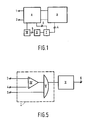
- Fig. 1 is a diagrammatic picture of the arrangement of an embodiment of a circuit arrangement according to the invention.
- FIG. 2 shows further details of the embodiment shown in Fig. 1;
- Figs. 3 and 4 show the shapes of voltages and currents in the DC-AC converter shown in Figs. 1 and 2, and
- Fig. 5 shows a preferred embodiment of the measuring circuit I.
- reference numeral 1 denotes a first terminal of a circuit A and 2 denotes a further terminal of circuit A. 1 and 2 are suitable for being connected to the terminals of a DC voltage source.
- Circuit A comprises a switching element for generating a current of alternating polarity by being alternately conducting and non-conducting with a frequency f.
- B is a load circuit comprising inductive means and lamp connection terminals. Load circuit B is coupled to circuit A.
- a lamp La is connected to the lamp connection terminals.
- III denotes a drive circuit for generating a drive signal for making the switching element of circuit A alternately conducting and non-conducting.
- I is a measuring circuit for generating a control signal which is dependent on a phase difference between a voltage across the load circuit B and a current through the load circuit B.
- the measuring circuit I is coupled to a current sensor and to a switching element of circuit A.
- An output of measuring circuit I is connected to an input of control circuit II.
- Control circuit II is a circuit for rendering the switching element non-conducting for the remainder of a period belonging to the frequency f of the switching element.
- an output of control circuit II is connected to an input of drive circuit III.
- Drive circuit III is connected to the switching elements of circuit A.
- the drive circuit When the input terminals 1 and 2 are connected to poles of a DC voltage source, the drive circuit renders the switching element in circuit A alternativeately conducting and non-conducting with a frequency f.
- a current J flows through the load circuit with a polarity which changes with the frequency f, while a periodic voltage is present between the ends of the load circuit B.
- the measuring circuit I generates a control signal which is dependent on this phase difference.
- the conrol circuit II will render the switching element non-conducting for the remainder of a period belonging to the frequency f of the switching element.
- the circuit A is formed by ends 1 and 2, switching elements S1 and S2, and diodes D1 and D2.
- Load circuit B consists of a coil L, lamp connection terminals K1 and K2, capacitors C1 and C2, and a current sensor SE.
- a lamp La may be connected to the load circuit.
- the coil L in this embodiment forms the inductive means.
- Input terminals 1 and 2 are interconnected by a series circuit of switching elements S1 and S2 in such a way that a main electrode of switching element S1 is connected to terminal 1 and a main electrode of switching element S2 to terminal 2.
- Switching element S1 is shunted by a diode D1 in such a way that an anode of the diode D1 is connected to a common point P of the two switching elements S1 and S2.
- Switching element S2 is shunted by a diode D2 in such a way that an anode of the diode D2 is connected to terminal 2.
- Switching element 52 is also shunted by a series circuit comprising the coil L, connection terminal K1, lamp La, connection terminal K2, capacitor C2, and current sensor SE, which in the embodiment shown is formed by a resistor.
- the lamp La is shunted by the capacitor C1.
- Both ends of the sensor SE are connected to separate inputs of the measuring circuit I.
- a further input of the measuring circuit I is connected to a control electrode of a switching element.
- An output of the drive circuit III is connected to a control electrode of the switching element S1, and a second output of the drive circuit III is connected to a control electrode of the switching element S2.
- the drive signal makes the switching elements S1 and S2 alternately conducting with a repetition frequency f.
- a common point P of the two switching elements is alternately connected to the negative and the positive pole of the DC voltage source.
- a substantially square-wave voltage Vp is present at point P with a repetition frequency f.
- This substantially square-wave voltage Vp causes a current J, whose polarity changes with the repetition frequency f, to flow in load circuit B.
- the measuring circuit I generates a control signal which depends on the phase difference between the substantially square-wave voltage Vp and the current J.
- the control circuit makes a switching element non-conducting for the remainder of the period belonging to the frequency f of the switching element. Rendering a switching element non conducting substantially coincides in time with a rising or falling edge of the substantially square-wave voltage Vp. This renders it possible, for example, to control the phase difference between the substantially square-wave voltage Vp and the alternating current J by making a conducting switching element non-conducting if the absolute instantaneous value of the alternating current J falls to below a reference level which is a measure for a minimum required phase difference.
- the horizontal axis shows the time dimension in relative measure and the vertical axis the current or voltage dimension in relative measure.
- J is the current flowing in the load circuit B.
- Vp is the substantially square-wave voltage present at the common point P of the two switching elements S1 and S2.
- e is the phase difference between Vp and J and g is a minimum required phase difference between Vp and j e ' is an instantaneous value of the current J coinciding in time with a rising edge of Vp; e ' at the same time is a measure for the phase difference between Vp and J.
- Ia is a current in circuit A. This current does not flow during one half of each period of Vp.
- IV is a comparator having inputs 3 and 4. An output of the comparator IV is connected to an input of logic AND gate V. Reference numeral 5 denotes another input of logic AND gate V. An output of V is connected to an input of control circuit II.
- input 4 is coupled to the current sensor SE while at input 3 a reference signal is present which is a measure for a minimum required value of the phase difference between Vp and J.
- Input 5 is coupled to a control electrode of a switching element.
- the value of the signal present at input 4 drops to below the value of the reference signal present at input 3. This causes the signal at the output of comparator IV to change from low to high. If the corresponding switching element, S1 or S2, is conducting, the signal at input 5 is high, so that also the signal at the output of the logic AND gate V changes from low to high.
- the signal at the output of logic AND gate V in this embodiment of the measuring circuit is the control signal and activates the control circuit II so that it renders the then conducting switching element non-conducting.
- phase difference between the periodic voltage Vp and the alternating current J is greater than the minimum required value, the signal at input 5 is low at the moment at which the signal at the output of comparator IV changes from low to high, since the relevant switching element is non-conducting then. In this situation the control signal at the output of logic AND gate V remains low and the control circuit II is not activated.
- the measuring circuit was designed as shown in Fig. 5.
- the frequency f was 28 kHz. It was found to be possible to remove a burning lamp from the lamp connection terminals without this abrupt change in the load of the circuit arrangement resulting in capacitive operation of the DC-AC converter.
Landscapes
- Circuit Arrangements For Discharge Lamps (AREA)
- Inverter Devices (AREA)
Applications Claiming Priority (4)
| Application Number | Priority Date | Filing Date | Title |
|---|---|---|---|
| NL8902940 | 1989-11-29 | ||
| NL8902940 | 1989-11-29 | ||
| NL9001242 | 1990-05-31 | ||
| NL9001242 | 1990-05-31 |
Publications (2)
| Publication Number | Publication Date |
|---|---|
| EP0430358A1 true EP0430358A1 (fr) | 1991-06-05 |
| EP0430358B1 EP0430358B1 (fr) | 1995-10-25 |
Family
ID=26646617
Family Applications (1)
| Application Number | Title | Priority Date | Filing Date |
|---|---|---|---|
| EP90203092A Expired - Lifetime EP0430358B1 (fr) | 1989-11-29 | 1990-11-23 | Dispositif de commutation |
Country Status (6)
| Country | Link |
|---|---|
| US (1) | US5075599A (fr) |
| EP (1) | EP0430358B1 (fr) |
| JP (1) | JP3176914B2 (fr) |
| KR (1) | KR100210548B1 (fr) |
| DE (1) | DE69023205T2 (fr) |
| HU (1) | HUT55935A (fr) |
Cited By (19)
| Publication number | Priority date | Publication date | Assignee | Title |
|---|---|---|---|---|
| EP0583838A2 (fr) * | 1992-08-20 | 1994-02-23 | Koninklijke Philips Electronics N.V. | Circuit ballast de lampe |
| US5345148A (en) * | 1992-02-18 | 1994-09-06 | Singapore Institute Of Standards And Industrial Research | DC-AC converter for igniting and supplying a gas discharge lamp |
| EP0641149A1 (fr) * | 1993-08-23 | 1995-03-01 | Koninklijke Philips Electronics N.V. | Régulation de puissance d'un onduleur pour une lampe à décharge |
| US5670849A (en) * | 1995-06-29 | 1997-09-23 | U.S. Philips Corporation | Circuit arrangement |
| US5925985A (en) * | 1996-07-27 | 1999-07-20 | Singapore Productivity And Standards Board | Electronic ballast circuit for igniting, supplying and dimming a gas discharge lamp |
| WO2001045241A1 (fr) * | 1999-12-18 | 2001-06-21 | Koninklijke Philips Electronics N.V. | Convertisseur a elements de circuit resonant |
| WO2001093379A1 (fr) * | 2000-05-30 | 2001-12-06 | Lempi @ S.A. | Alimentation a decoupage pour lampe a decharge et procede d'alimentation d'une lampe |
| WO2003098790A1 (fr) * | 2002-05-15 | 2003-11-27 | Philips Intellectual Property & Standards Gmbh | Agencement de circuit pour convertisseur resonant et procede de fonctionnement de ce convertisseur |
| EP1372362A2 (fr) * | 2002-06-11 | 2003-12-17 | Patent-Treuhand-Gesellschaft für elektrische Glühlampen mbH | Circuit muni d'une régulation de courant et d'une détection d'approche de fonctionnement en mode capacitif pour alimenter une lampe à décharge |
| EP1377135A2 (fr) * | 2002-06-11 | 2004-01-02 | Patent-Treuhand-Gesellschaft für elektrische Glühlampen mbH | Circuit muni d'une détection d'approche de fonctionnement en mode capacitif pour alimenter une lampe à décharge |
| WO2004105226A1 (fr) | 2003-05-23 | 2004-12-02 | Auckland Uniservices Limited | Convertisseur auto-oscillant a regulation de frequence |
| US6888320B2 (en) | 1999-06-08 | 2005-05-03 | Lempi Sa | Switching power supply for discharge lamp and method for powering a lamp |
| ITMI20082356A1 (it) * | 2008-12-30 | 2010-06-30 | St Microelectronics Srl | Controllo di un sistema a commutazione risonante con monitoraggio della corrente di lavoro in una finestra di osservazione |
| US8093758B2 (en) | 2003-05-23 | 2012-01-10 | Auckland Uniservices Limited | Method and apparatus for control of inductively coupled power transfer systems |
| EP2518889A1 (fr) * | 2011-04-29 | 2012-10-31 | AEG Power Solutions B.V. | Onduleur à circuit oscillant doté d'un point de travail réglable |
| US8749209B2 (en) | 2008-05-05 | 2014-06-10 | Infineon Technologies Austria Ag | System and method for providing adaptive dead times |
| WO2019138251A1 (fr) * | 2018-01-15 | 2019-07-18 | Tdk-Lambda Uk Limited | Appareil et procédés à utiliser dans un convertisseur résonnant |
| EP2445098B1 (fr) * | 2010-10-25 | 2019-08-07 | STMicroelectronics Srl | Dispositif de contrôle pour convertisseur résonnant |
| GB2584217A (en) * | 2018-01-15 | 2020-11-25 | Tdk Lambda Uk Ltd | Apparatus and methods for use in a resonant converter |
Families Citing this family (19)
| Publication number | Priority date | Publication date | Assignee | Title |
|---|---|---|---|---|
| SG48126A1 (en) * | 1991-11-13 | 1998-04-17 | Philips Electronics Nv | Circuit arrangement |
| US5475284A (en) * | 1994-05-03 | 1995-12-12 | Osram Sylvania Inc. | Ballast containing circuit for measuring increase in DC voltage component |
| FR2721475B1 (fr) * | 1994-06-15 | 1996-07-19 | Sgs Thomson Microelectronics | Circuit de commande de commutation et dispositif de commande pour lampe fluorescente à basse pression. |
| DE4425890A1 (de) * | 1994-07-11 | 1996-01-18 | Priamos Licht Ind & Dienstleis | Schaltungsanordnung für den Betrieb einer Entladungslampe |
| US5696431A (en) * | 1996-05-03 | 1997-12-09 | Philips Electronics North America Corporation | Inverter driving scheme for capacitive mode protection |
| US5717295A (en) * | 1996-05-10 | 1998-02-10 | General Electric Company | Lamp power supply circuit with feedback circuit for dynamically adjusting lamp current |
| US5703439A (en) * | 1996-05-10 | 1997-12-30 | General Electric Company | Lamp power supply circuit with electronic feedback circuit for switch control |
| US5719472A (en) * | 1996-05-13 | 1998-02-17 | General Electric Company | High voltage IC-driven half-bridge gas discharge ballast |
| US5859504A (en) * | 1996-10-01 | 1999-01-12 | General Electric Company | Lamp ballast circuit with cathode preheat function |
| DE19709545A1 (de) * | 1997-03-07 | 1998-09-10 | Patent Treuhand Ges Fuer Elektrische Gluehlampen Mbh | Schaltsteuerung einer Betriebsschaltung |
| US6326740B1 (en) | 1998-12-22 | 2001-12-04 | Philips Electronics North America Corporation | High frequency electronic ballast for multiple lamp independent operation |
| JP2003530813A (ja) | 2000-04-10 | 2003-10-14 | コーニンクレッカ フィリップス エレクトロニクス エヌ ヴィ | 制御回路を有するエネルギー変換器 |
| EP1277374B1 (fr) | 2000-04-10 | 2005-11-09 | Koninklijke Philips Electronics N.V. | Ballast a detecteur de crete |
| TW319487U (en) * | 2000-09-27 | 1997-11-01 | Patent Treuhand Ges Fuer Elek Sche Gluhlampen Mbh Co Ltd | Operating device for electrical lamps |
| WO2002035894A1 (fr) * | 2000-10-27 | 2002-05-02 | Koninklijke Philips Electronics N.V. | Circuit |
| CN1910965A (zh) * | 2004-01-23 | 2007-02-07 | 皇家飞利浦电子股份有限公司 | 气体放电灯的高频驱动器 |
| DE102004037388B4 (de) * | 2004-08-02 | 2008-05-29 | Infineon Technologies Ag | Verfahren zur Detektion eines Nicht-Nullspannungsschaltbetriebs eines Vorschaltgeräts für Leuchtstofflampen und Vorschaltgerät |
| US7279847B2 (en) * | 2005-03-31 | 2007-10-09 | Nerone Louis R | Pulse starting circuit |
| US9685867B2 (en) | 2014-08-22 | 2017-06-20 | Stmicroelectronics International N.V. | Electrical power supply |
Citations (3)
| Publication number | Priority date | Publication date | Assignee | Title |
|---|---|---|---|---|
| EP0059064B1 (fr) * | 1981-02-21 | 1985-10-02 | THORN EMI plc | Circuit de démarrage et d'exploitation de lampes |
| EP0178852A1 (fr) * | 1984-10-16 | 1986-04-23 | ADVANCE TRANSFORMER CO. (a Division of Philips Electronics North America Corporation) | Circuit ballast électronique prévu pour lampes fluorescentes |
| EP0338109A1 (fr) * | 1988-04-20 | 1989-10-25 | Zumtobel Aktiengesellschaft | Convertisseur pour lampe à décharge |
Family Cites Families (3)
| Publication number | Priority date | Publication date | Assignee | Title |
|---|---|---|---|---|
| US4887007A (en) * | 1987-02-18 | 1989-12-12 | U.S. Philips Corporation | DC-AC converter for supplying a gas and/or vapour discharge lamp |
| NL8702383A (nl) * | 1987-10-07 | 1989-05-01 | Philips Nv | Elektrische inrichting voor het ontsteken en voeden van een gasontladingslamp. |
| NL8800015A (nl) * | 1988-01-06 | 1989-08-01 | Philips Nv | Elektrische inrichting voor het ontsteken en voeden van een gasontladingslamp. |
-
1990
- 1990-11-16 US US07/614,887 patent/US5075599A/en not_active Expired - Fee Related
- 1990-11-23 DE DE69023205T patent/DE69023205T2/de not_active Expired - Fee Related
- 1990-11-23 EP EP90203092A patent/EP0430358B1/fr not_active Expired - Lifetime
- 1990-11-26 HU HU907649A patent/HUT55935A/hu unknown
- 1990-11-26 JP JP31818990A patent/JP3176914B2/ja not_active Expired - Fee Related
- 1990-11-27 KR KR1019900019245A patent/KR100210548B1/ko not_active IP Right Cessation
Patent Citations (3)
| Publication number | Priority date | Publication date | Assignee | Title |
|---|---|---|---|---|
| EP0059064B1 (fr) * | 1981-02-21 | 1985-10-02 | THORN EMI plc | Circuit de démarrage et d'exploitation de lampes |
| EP0178852A1 (fr) * | 1984-10-16 | 1986-04-23 | ADVANCE TRANSFORMER CO. (a Division of Philips Electronics North America Corporation) | Circuit ballast électronique prévu pour lampes fluorescentes |
| EP0338109A1 (fr) * | 1988-04-20 | 1989-10-25 | Zumtobel Aktiengesellschaft | Convertisseur pour lampe à décharge |
Cited By (34)
| Publication number | Priority date | Publication date | Assignee | Title |
|---|---|---|---|---|
| US5345148A (en) * | 1992-02-18 | 1994-09-06 | Singapore Institute Of Standards And Industrial Research | DC-AC converter for igniting and supplying a gas discharge lamp |
| EP0583838A2 (fr) * | 1992-08-20 | 1994-02-23 | Koninklijke Philips Electronics N.V. | Circuit ballast de lampe |
| EP0583838A3 (fr) * | 1992-08-20 | 1994-03-09 | Koninklijke Philips Electronics N.V. | Circuit ballast de lampe |
| EP0641149A1 (fr) * | 1993-08-23 | 1995-03-01 | Koninklijke Philips Electronics N.V. | Régulation de puissance d'un onduleur pour une lampe à décharge |
| BE1007458A3 (nl) * | 1993-08-23 | 1995-07-04 | Philips Electronics Nv | Schakelinrichting. |
| US5670849A (en) * | 1995-06-29 | 1997-09-23 | U.S. Philips Corporation | Circuit arrangement |
| US5925985A (en) * | 1996-07-27 | 1999-07-20 | Singapore Productivity And Standards Board | Electronic ballast circuit for igniting, supplying and dimming a gas discharge lamp |
| US6888320B2 (en) | 1999-06-08 | 2005-05-03 | Lempi Sa | Switching power supply for discharge lamp and method for powering a lamp |
| WO2001045241A1 (fr) * | 1999-12-18 | 2001-06-21 | Koninklijke Philips Electronics N.V. | Convertisseur a elements de circuit resonant |
| US6466456B2 (en) | 1999-12-18 | 2002-10-15 | Koninklijke Philips Electronics N.V. | Converter with resonant circuit elements for determing load type |
| KR100747424B1 (ko) * | 1999-12-18 | 2007-08-09 | 코닌클리케 필립스 일렉트로닉스 엔.브이. | 공진 회로 소자들을 갖는 컨버터 |
| WO2001093379A1 (fr) * | 2000-05-30 | 2001-12-06 | Lempi @ S.A. | Alimentation a decoupage pour lampe a decharge et procede d'alimentation d'une lampe |
| WO2003098790A1 (fr) * | 2002-05-15 | 2003-11-27 | Philips Intellectual Property & Standards Gmbh | Agencement de circuit pour convertisseur resonant et procede de fonctionnement de ce convertisseur |
| US7190596B2 (en) | 2002-05-15 | 2007-03-13 | Koninklijke Philips Electronics N.V. | Resonant converter with phase controlled switching |
| EP1372362A3 (fr) * | 2002-06-11 | 2006-04-05 | Patent-Treuhand-Gesellschaft für elektrische Glühlampen mbH | Circuit muni d'une régulation de courant et d'une détection d'approche de fonctionnement en mode capacitif pour alimenter une lampe à décharge |
| EP1377135A2 (fr) * | 2002-06-11 | 2004-01-02 | Patent-Treuhand-Gesellschaft für elektrische Glühlampen mbH | Circuit muni d'une détection d'approche de fonctionnement en mode capacitif pour alimenter une lampe à décharge |
| EP1372362A2 (fr) * | 2002-06-11 | 2003-12-17 | Patent-Treuhand-Gesellschaft für elektrische Glühlampen mbH | Circuit muni d'une régulation de courant et d'une détection d'approche de fonctionnement en mode capacitif pour alimenter une lampe à décharge |
| EP1377135A3 (fr) * | 2002-06-11 | 2006-05-03 | Patent-Treuhand-Gesellschaft für elektrische Glühlampen mbH | Circuit muni d'une détection d'approche de fonctionnement en mode capacitif pour alimenter une lampe à décharge |
| US8050068B2 (en) | 2003-05-23 | 2011-11-01 | Auckland Uniservices Limited | Variable reactive element in a resonant converter circuit |
| EP1634366A4 (fr) * | 2003-05-23 | 2007-11-07 | Auckland Uniservices Ltd | Convertisseur auto-oscillant a regulation de frequence |
| WO2004105226A1 (fr) | 2003-05-23 | 2004-12-02 | Auckland Uniservices Limited | Convertisseur auto-oscillant a regulation de frequence |
| EP1634366A1 (fr) * | 2003-05-23 | 2006-03-15 | Auckland Uniservices Limited | Convertisseur auto-oscillant a regulation de frequence |
| US8093758B2 (en) | 2003-05-23 | 2012-01-10 | Auckland Uniservices Limited | Method and apparatus for control of inductively coupled power transfer systems |
| US8749209B2 (en) | 2008-05-05 | 2014-06-10 | Infineon Technologies Austria Ag | System and method for providing adaptive dead times |
| US9473025B2 (en) | 2008-05-05 | 2016-10-18 | Infineon Technologies Austria Ag | System and method for providing adaptive dead times for a half bridge circuit |
| EP2205048A1 (fr) * | 2008-12-30 | 2010-07-07 | STMicroelectronics Srl | Commande d'un système de commutation résonant avec surveillance du courant de travail dans une fenêtre d'observation |
| ITMI20082356A1 (it) * | 2008-12-30 | 2010-06-30 | St Microelectronics Srl | Controllo di un sistema a commutazione risonante con monitoraggio della corrente di lavoro in una finestra di osservazione |
| EP2445098B1 (fr) * | 2010-10-25 | 2019-08-07 | STMicroelectronics Srl | Dispositif de contrôle pour convertisseur résonnant |
| EP2518889A1 (fr) * | 2011-04-29 | 2012-10-31 | AEG Power Solutions B.V. | Onduleur à circuit oscillant doté d'un point de travail réglable |
| US8976544B2 (en) | 2011-04-29 | 2015-03-10 | Aeg Power Solutions B.V. | Resonant circuit inverter with controllable operating point |
| WO2019138251A1 (fr) * | 2018-01-15 | 2019-07-18 | Tdk-Lambda Uk Limited | Appareil et procédés à utiliser dans un convertisseur résonnant |
| GB2584217A (en) * | 2018-01-15 | 2020-11-25 | Tdk Lambda Uk Ltd | Apparatus and methods for use in a resonant converter |
| US11264913B2 (en) | 2018-01-15 | 2022-03-01 | Tdk-Lambda Uk Limited | Apparatus and methods for use in a resonant converter |
| GB2584217B (en) * | 2018-01-15 | 2022-09-14 | Tdk Lambda Uk Ltd | Apparatus and methods for use in a resonant converter |
Also Published As
| Publication number | Publication date |
|---|---|
| KR100210548B1 (ko) | 1999-07-15 |
| HUT55935A (en) | 1991-06-28 |
| DE69023205D1 (de) | 1995-11-30 |
| US5075599A (en) | 1991-12-24 |
| JPH03246892A (ja) | 1991-11-05 |
| EP0430358B1 (fr) | 1995-10-25 |
| KR910011092A (ko) | 1991-06-29 |
| JP3176914B2 (ja) | 2001-06-18 |
| DE69023205T2 (de) | 1996-05-30 |
Similar Documents
| Publication | Publication Date | Title |
|---|---|---|
| EP0430358B1 (fr) | Dispositif de commutation | |
| US5608294A (en) | High pressure lamp operating circuit with suppression of lamp flicker | |
| EP0482705B1 (fr) | Dispositif de commutation | |
| US5075602A (en) | Discharge lamp control circuit arrangement | |
| US8054003B2 (en) | Switch-off time regulation system for an inverter for driving a lamp | |
| KR100278528B1 (ko) | 램프 점화 작동 장치 | |
| US4029993A (en) | Two level inverter circuit | |
| US6317339B1 (en) | Method of controlling electric power supply apparatus with electric power converter circuit | |
| US5670849A (en) | Circuit arrangement | |
| US5844380A (en) | Circuit arrangement for ingniting and supplying power to a lamp | |
| US7064499B2 (en) | Method for operating at least one low-pressure discharge lamp and operating device for at least one low-pressure discharge lamp | |
| US7812612B2 (en) | Method and apparatus for monitoring the operation of a gas discharge lamp | |
| EP0401911B1 (fr) | Dispositif de commutation | |
| US6134132A (en) | Circuit arrangement | |
| US5477109A (en) | Discharge lamp fast preheat circuit independent of type of ballast | |
| CN108594100B (zh) | 电灯灯管寿命的检测电路及电灯 | |
| JP3557665B2 (ja) | 照明装置 | |
| JPH06338397A (ja) | 放電灯点灯装置および照明装置 | |
| JP3056802B2 (ja) | インバータ装置 | |
| JP3356216B2 (ja) | 放電灯点灯装置 | |
| KR890003956B1 (ko) | 방전등 점등장치 | |
| JPH0735359Y2 (ja) | 放電灯の点灯装置 | |
| JPS60137063A (ja) | サイリスタのゲ−トトリガ装置 | |
| JPS6152161A (ja) | 電源装置 | |
| JPS5916400B2 (ja) | 放電灯点灯装置 |
Legal Events
| Date | Code | Title | Description |
|---|---|---|---|
| PUAI | Public reference made under article 153(3) epc to a published international application that has entered the european phase |
Free format text: ORIGINAL CODE: 0009012 |
|
| AK | Designated contracting states |
Kind code of ref document: A1 Designated state(s): BE DE FR GB IT NL |
|
| 17P | Request for examination filed |
Effective date: 19911204 |
|
| 17Q | First examination report despatched |
Effective date: 19931012 |
|
| GRAA | (expected) grant |
Free format text: ORIGINAL CODE: 0009210 |
|
| AK | Designated contracting states |
Kind code of ref document: B1 Designated state(s): BE DE FR GB IT NL |
|
| REF | Corresponds to: |
Ref document number: 69023205 Country of ref document: DE Date of ref document: 19951130 |
|
| ITF | It: translation for a ep patent filed | ||
| ET | Fr: translation filed | ||
| PLBE | No opposition filed within time limit |
Free format text: ORIGINAL CODE: 0009261 |
|
| STAA | Information on the status of an ep patent application or granted ep patent |
Free format text: STATUS: NO OPPOSITION FILED WITHIN TIME LIMIT |
|
| 26N | No opposition filed | ||
| NLT1 | Nl: modifications of names registered in virtue of documents presented to the patent office pursuant to art. 16 a, paragraph 1 |
Owner name: KONINKLIJKE PHILIPS ELECTRONICS N.V. |
|
| REG | Reference to a national code |
Ref country code: FR Ref legal event code: CD |
|
| PGFP | Annual fee paid to national office [announced via postgrant information from national office to epo] |
Ref country code: BE Payment date: 19981028 Year of fee payment: 9 |
|
| PGFP | Annual fee paid to national office [announced via postgrant information from national office to epo] |
Ref country code: NL Payment date: 19981130 Year of fee payment: 9 |
|
| PG25 | Lapsed in a contracting state [announced via postgrant information from national office to epo] |
Ref country code: BE Free format text: LAPSE BECAUSE OF NON-PAYMENT OF DUE FEES Effective date: 19991130 |
|
| BERE | Be: lapsed |
Owner name: KONINKLIJKE PHILIPS ELECTRONICS N.V. Effective date: 19991130 |
|
| PG25 | Lapsed in a contracting state [announced via postgrant information from national office to epo] |
Ref country code: NL Free format text: LAPSE BECAUSE OF NON-PAYMENT OF DUE FEES Effective date: 20000601 |
|
| NLV4 | Nl: lapsed or anulled due to non-payment of the annual fee |
Effective date: 20000601 |
|
| PGFP | Annual fee paid to national office [announced via postgrant information from national office to epo] |
Ref country code: FR Payment date: 20011122 Year of fee payment: 12 |
|
| PGFP | Annual fee paid to national office [announced via postgrant information from national office to epo] |
Ref country code: GB Payment date: 20011130 Year of fee payment: 12 |
|
| REG | Reference to a national code |
Ref country code: GB Ref legal event code: IF02 |
|
| PGFP | Annual fee paid to national office [announced via postgrant information from national office to epo] |
Ref country code: DE Payment date: 20020116 Year of fee payment: 12 |
|
| REG | Reference to a national code |
Ref country code: GB Ref legal event code: 746 Effective date: 20020917 |
|
| REG | Reference to a national code |
Ref country code: FR Ref legal event code: D6 |
|
| PG25 | Lapsed in a contracting state [announced via postgrant information from national office to epo] |
Ref country code: GB Free format text: LAPSE BECAUSE OF NON-PAYMENT OF DUE FEES Effective date: 20021123 |
|
| PG25 | Lapsed in a contracting state [announced via postgrant information from national office to epo] |
Ref country code: DE Free format text: LAPSE BECAUSE OF NON-PAYMENT OF DUE FEES Effective date: 20030603 |
|
| GBPC | Gb: european patent ceased through non-payment of renewal fee | ||
| PG25 | Lapsed in a contracting state [announced via postgrant information from national office to epo] |
Ref country code: FR Free format text: LAPSE BECAUSE OF NON-PAYMENT OF DUE FEES Effective date: 20030731 |
|
| REG | Reference to a national code |
Ref country code: FR Ref legal event code: ST |
|
| PG25 | Lapsed in a contracting state [announced via postgrant information from national office to epo] |
Ref country code: IT Free format text: LAPSE BECAUSE OF NON-PAYMENT OF DUE FEES Effective date: 20051123 |