EP0424331B1 - MOS-IC mit geschalteten Kondensatoren und mit Vollwellengleichrichtungs- und Integrations-Funktion - Google Patents
MOS-IC mit geschalteten Kondensatoren und mit Vollwellengleichrichtungs- und Integrations-Funktion Download PDFInfo
- Publication number
- EP0424331B1 EP0424331B1 EP90830441A EP90830441A EP0424331B1 EP 0424331 B1 EP0424331 B1 EP 0424331B1 EP 90830441 A EP90830441 A EP 90830441A EP 90830441 A EP90830441 A EP 90830441A EP 0424331 B1 EP0424331 B1 EP 0424331B1
- Authority
- EP
- European Patent Office
- Prior art keywords
- signal
- capacitor
- circuit
- input
- clock
- Prior art date
- Legal status (The legal status is an assumption and is not a legal conclusion. Google has not performed a legal analysis and makes no representation as to the accuracy of the status listed.)
- Expired - Lifetime
Links
Images


Classifications
-
- G—PHYSICS
- G01—MEASURING; TESTING
- G01R—MEASURING ELECTRIC VARIABLES; MEASURING MAGNETIC VARIABLES
- G01R19/00—Arrangements for measuring currents or voltages or for indicating presence or sign thereof
- G01R19/22—Arrangements for measuring currents or voltages or for indicating presence or sign thereof using conversion of AC into DC
-
- F—MECHANICAL ENGINEERING; LIGHTING; HEATING; WEAPONS; BLASTING
- F02—COMBUSTION ENGINES; HOT-GAS OR COMBUSTION-PRODUCT ENGINE PLANTS
- F02B—INTERNAL-COMBUSTION PISTON ENGINES; COMBUSTION ENGINES IN GENERAL
- F02B1/00—Engines characterised by fuel-air mixture compression
- F02B1/02—Engines characterised by fuel-air mixture compression with positive ignition
- F02B1/04—Engines characterised by fuel-air mixture compression with positive ignition with fuel-air mixture admission into cylinder
Definitions
- the present invention relates to a circuit for rectifying and integrating an alternating input signal of the kind defined in the first portion of Claim 1.
- circuits for detecting alternating signals greatly affected by noise which are generated, for example, by sensors operating in difficult environments.
- circuits including a full-wave rectifier and an integrator as basic components are used.
- a circuit of this type is used, for example, in devices for detecting pinking in Otto engines, as described, for example in EP-A-0 421 952.
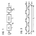
- Figure 1 of the appended drawings shows such a known arrangement including a piezoelectric accelerometric sensor S whose signal is processed by a band-pass filter 1 and then by a full-wave rectifier 2 and an integrator 3 which is activated cyclically for a preset time period Ta.
- the signal V0 output by the integrator 3 provides information relating to the intensity of the sensor signal in the region of the resonance frequencies typical of pinking.
- a typical problem in the circuit 1 to 3 of Figure 1 is the integration of the inevitable offset voltage affecting the input signal of the integrator and of the offset voltage generated in the integrator itself, which may lead to the saturation of the output signal. This problem leads to the need to use low-offset components or to use techniques for automatically cancelling out the offset.
- this can be formed by conventional circuitry with discrete components.
- the following is concerned with solutions which enable the circuit to be produced in integrated form, specifically by CMOS technology and particularly with the use of circuitry of the type with switched capacitors.
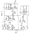
- FIG. 2 of the appended drawings shows a prior art embodiment of the rectifier and the integrator of Figure 1 with switched-capacitor circuitry which can be produced in integrated form.
- the rectifier circuit 2 has an input, indicated I, and includes a circuit 10 for determining the polarity of the input signal V in and an amplifier circuit, generally indicated 11.
- the polarity-determining circuit 10 comprises:
- the switches S1, S3 and S2, S10 respectively are piloted in an on-off manner by two clock signals, indicated, ⁇ 1 and ⁇ 2 , which have the same frequency but are out of phase so that their respective active periods ("on" times, that is, the periods when the associated switches are closed) alternate and do not overlap, as shown by the corresponding waveforms shown in Figure 3.
- ⁇ 1 and ⁇ 2 which have the same frequency but are out of phase so that their respective active periods ("on" times, that is, the periods when the associated switches are closed) alternate and do not overlap, as shown by the corresponding waveforms shown in Figure 3.
- the amplifier circuit 11 comprises:
- S4 and S12 are piloted by the clock or phase signal ⁇ 1 , whilst S5, S11 and S13 are piloted by the phase signal ⁇ 2.
- S7 and S8 are piloted by the output A of the flip-flop 12, whilst S6 and S9 are piloted by the output A of the flip-flop.
- the outputs A and A of the flip-flop 12 control the switches S6, S7, S8 and S9 so that the operational amplifier A1 is connected as a non-inverting amplifier: during each "on" period of the phase signal ⁇ 2, the capacitor C2 samples the signal V in whilst, during each next "on” period of ⁇ 1, it outputs its charge.
- the switches S6, S7, S8 and S9 are controlled so that the operational amplifier A1 constitutes an inverting amplifier: in this case, the capacitor C2 samples the signal V in and outputs its own charge during each "on" period of the phase ⁇ 1.
- the integrator 3 comprises:
- S14 and S17 are piloted by the phase signal ⁇ 1, whilst S15 and S16 are piloted by the phase signal ⁇ 2.
- S18 and S20 are piloted by a signal R which is normally at level "one" and is at low level during the time period T a corresponding to the period during which the integrator 3 is required to integrate.
- This signal like the phase signals ⁇ 1 and ⁇ 2, is generated by a control circuit, generally indicated CU in Figure 2, the details of which, however, are not essential for the purposes of the present description.
- the switch S19 of the integrator 3 is piloted by a signal R complementary to R.
- the rectifier 2 outputs its signal during each "on" period of ⁇ 1 : during each of these periods, the integrator 3 zeroes its own offset voltage by means of S17 which puts A2 into the voltage-follower configuration.
- the integrator 3 samples the voltage output by the rectifier 2, by means of the capacitor C4.
- the capacitor C5 acts as the integrating and memory element. It is discharged only at the end of the integration period T a by means of the switches S18, S19, S20 which are controlled by the signals R (reset) and R (integration signal).
- switches S19 and S16 can be replaced by a single switch controlled by the conjunction (AND) of the signals R and ⁇ 2.
- the capacitor C3 acts as an integrating and memory element which is zeroed at the end of the integration period T a by means of the switches S19 and S20 piloted by the signals R and R.
- the rectified and integrated signal is available at the output of the amplifier A1.
- the prior art circuit according to Figure 4 has a much simplified structure but also has a disadvantage.
- the input signal V in is sampled during the "on" periods of the phase signal ⁇ 1 or ⁇ 2 in dependence on its polarity. This presupposes that the signal V in is always available in both the phases ⁇ 1 and ⁇ 2.
- a useful signal is not always available throughout the clock period of the switched-capacitor system. It is thus convenient always to be able to sample the input signal in the same phase, regardless of its polarity. This would also enable the cancellation, during the other phase, of any offset voltages in the circuit upstream which generates the signal V in .
- This function is particularly important when signals must be integrated over long periods of time. In fact, in such cases, the minimizing of the offset voltages of the input signal and of the components for processing it (amplifiers, comparators, etc.) becomes one of the main objectives for ensuring the correct operation of the device.
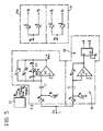
- the object of the present invention is to provide a new circuit in which the full-wave rectification and integration of the input signal are achieved by a single operational amplifier and in which the input signal is always sampled during the same phase, regardless of its polarity.
- This object is achieved, according to the invention, by means of a circuit whose main characteristics are defined in appended claim 1.
- the circuit according to the invention is insensitive to the stray capacitances and offsets of its active components (the comparator and operational amplifier).
- the input signal is sampled during only one phase of the clock which regulates the operation of the switched-capacitor circuit.
- the circuit for determining the polarity of the input signal comprises a comparator circuit 10 identical to that described above, connected to a flip-flop circuit 12 which is preferably of the D type.
- the clock input of the flip-flop is piloted by the signal ⁇ 2 which is complementary to the phase, signal ⁇ 2 .
- the outputs of the flip-flop 12 are indicated Q and Q .
- the circuit of Figure 5 includes two multiplexers MA and MB each having two inputs for receiving the clock signals ⁇ 1 and ⁇ 2 respectively, and an output.
- two controlled switches S a and S b are provided between its ⁇ 1 and ⁇ 2 inputs and its output and are piloted by the outputs Q and Q of the flip-flop 12.
- two controlled switches S c and S d are provided between the ⁇ 1 and ⁇ 2 inputs and the output of MB and are piloted by Q and Q respectively.
- the rectifier-integrator circuit 2, 3 includes a single operational amplifier A1 with associated capacitors C2 and C3 and controlled switches S12, S13, S18, S19 and S20, arranged as in the diagram of Figure 4. it will be noted that in the diagram of Figure 5, however, the switches S12 and S13 are piloted by the signals output by the multiplexers MA and MB.
- R is at level "1"
- S19 is closed
- S20 and S18 are open.
- the input signal V in is sampled during the "on" times of the phase signal ⁇ 2 and, in the same time periods, the comparator circuit 10 determines the polarity of the input signal.
- the signal output by the comparator circuit 10 appears on the line Q of the flip-flop 12 at the end of each "on" time of the phase signal ⁇ 2 (the leading edge of ⁇ 2) and is stored for a period.
- the multiplexers MA and MB cause the phase ⁇ A to coincide with the phase ⁇ 1 and the phase ⁇ B to coincide with the phase ⁇ 2.
- the rectifier-integrator circuit therefore assumes a configuraton such that the input signal V in is integrated by means of the integration capacitor C3 in non-inverting mode during the phase ⁇ 1.
- the multiplexers MA and MB cause the phase ⁇ A to coincide with the phase ⁇ 2 and the phase ⁇ B to coincide with the phase ⁇ 1 .
- the capacitor C2 samples and transfers its charge to the capacitor C3 during the phase ⁇ 2 and the latter integrates the signal in inverting mode.
- the signal output by the rectifier-integrator circuit is available at the output of A1 during the phase ⁇ A .
- the integration capacitor C3 is discharged during the phases in which integration is not being carried out, that is, outside the time window T a or rather when the signal R is at level "1" (S18 and S20 closed, S19 open). This capacitor is thus discharged at the input voltage of the operational amplifier A1 which is equal to the offset of that operational amplifier. The offset is thus automatically cancelled out, eliminating any chance of errors in the next integration phase.
- the switched-capacitor circuit of Figure 5 performs the full-wave rectification and integration functions by means of a single operational amplifier which effects an inverting or non-inverting integration according to the polarity of the input signal.
- the input signal is sampled in only one phase, enabling the cancellation in the other phase of the offset in the circuits upstream which output the signal V in to be rectified and integrated.
Landscapes
- Engineering & Computer Science (AREA)
- Power Engineering (AREA)
- Physics & Mathematics (AREA)
- General Physics & Mathematics (AREA)
- Filters That Use Time-Delay Elements (AREA)
- Arrangements For Transmission Of Measured Signals (AREA)
- Control Of Amplification And Gain Control (AREA)
- Rectifiers (AREA)
- Measurement Of Current Or Voltage (AREA)
Claims (5)
- Schaltungsanordnung zur Gleichrichtung und Integration eines Wechseleingangssignals (Vin) enthaltend:
einen Eingangsanschluß (I),
einen Operationsverstärker (A1),
einen ersten Kondensator (C2) zwischen dem Eingangsanschluß (I) und dem invertierenden Eingang des Operationsverstärkers (A1) und einen zweiten Kondensator (C3) zwischen dem invertierenden Eingang und dem Ausgang des Operationsverstärkers (A1),
erste und zweite gesteuerte Schalter (S7, S6) zwischen Erde und dem Belag des ersten Kondensators (C2), der dem Eingangsanschluß (I) zugewandt ist bzw. zwischen dem Eingangsanschluß (I) und dem ersten Kondensator (C2),
dritte und vierte gesteuerte Schalter (S12, S13) in Reihe bzw. parallel zu dem zweiten Kondensator (C3),
Steuerschaltungsanordnungen (CU, 10, MA, MB) zur Erzeugung von Steuersignalen (φ₁, φ₂, φA, φB) für die Schalter (S7, S6, S12, S13) mit
einer Taktsignalgeneratorschaltung (CU) die für die Erzeugung von ersten und zweiten Takt- oder Phasensignalen (φ₁, φ₂) eingerichtet ist, die die gleiche Frequenz haben aber außer Phase sind, so daß die jeweiligen aktiven Perioden wechseln und sich nicht überlappen,
dadurch gekennzeichnet,
daß die Steuerschaltungsanordnungen (CU, 10, 12, MA, MB) so angeordnet sind, daß sie den ersten und zweiten Schalter (S7, S6) mit ersten bzw. zweiten Takt- oder Phasensignalen (φ₁, φ₂) versorgen und den dritten und vierten Schalter (S12, S13) jeweils mit ersten und zweiten Steuersignalen (φA, φB) versorgen, die mit den ersten bzw. zweiten Taktsignalen (φ₁, φ₂) übereinstimmen, wenn das Eingangssignal (Vin) die eine Polarität hat, die aber mit den zweiten bzw. ersten Taktsignalen (φ₂, φ₁) übereinstimmen, wenn das Eingangssignal (Vin) die entgegengesetzte Polarität hat. - Schaltungsanordnung nach Anspruch 1,
dadurch gekennzeichnet,
daß die Steuerschaltungsanordnungen enthalten:
eine polaritätsbestimmende Schaltung (10, 12), die für die Erzeugung eines logischen Signals zum Anzeigen der Polarität des Eingangssignals (Vin) eingerichtet ist, und
Multiplexerschaltungsanordnungen (MA, MB), die mit der Taktsignalgeneratorschaltung (CU) verbunden sind und von der polaritätsbestimmenden Schaltung (10, 12) gesteuert werden. - Schaltungsanordnung nach Anspruch 2,
dadurch gekennzeichnet,
daß die polaritätsbestimmende Schaltung (10, 12) enthält:
eine Komparatorschaltung (CO1) mit einem invertierenden Eingang und einem nichtinvertierenden Eingang,
einen Kondensator (C1), der zwischen dem Eingangsanschluß (I) und dem invertierenden Eingang der Komparatorschaltung (CO1) angeschlossen ist,
erste und zweite Schalter (S1, S2), die von den ersten bzw. zweiten Signalen (φ₁, φ₂) gesteuert werden und zwischen Erde und dem Belag des Kondensators (C1), der dem Eingangsanschluß (I) zugewandt ist, und zwischen dem Eingangsanschluß (I) und dem Kondensator (C1) angeordnet sind und
einen dritten gesteuerten Schalter (S3), der für die Steuerung durch das erste Taktsignal (φ₁) vorgesehen ist und zwischen dem invertierenden Eingang und dem Ausgang der Komparatorschaltung (CO1) angeordnet ist. - Schaltungsanordnung nach Anspruch 3,
dadurch gekennzeichnet,
daß der Ausgang der Komparatorschaltung (CO1) mit einem D-Flip-Flop (12) verbunden ist, dessen Takteingang von einem Signal (φ ₂) komplementär zum zweiten Taktsignal (φ₂) beaufschlagt ist. - Schaltungsanordnung nach Anspruch 1,
dadurch gekennzeichnet,
daß ein fünfter und ein sechster gesteuerter Schalter (S18, S19) parallel bwz. in Serie mit dem zweiten Kondensator (C3) und
ein siebter gesteuerter Schalter (S20) zwischen dem zweiten Kondensator (C3) und Erde vorgesehen sind,
wobei der fünfte und sechste Schalter (S18, S20) so gesteuert werden, daß sie in jeder Zeitperiode (Ta), in der das Eingangssignal (Vin) integriert wird, geöffnet sind, während der sechste Schalter (S19) für die Steuerung in komplementärer Weise bestimmt ist.
Applications Claiming Priority (2)
| Application Number | Priority Date | Filing Date | Title |
|---|---|---|---|
| IT06788789A IT1238117B (it) | 1989-10-16 | 1989-10-16 | Circuito a condensatori commutati, integrabile in tecnologia mos, con funzione di raddrizzatore a doppia semionda e di integratore |
| IT6788789 | 1989-10-16 |
Publications (2)
| Publication Number | Publication Date |
|---|---|
| EP0424331A1 EP0424331A1 (de) | 1991-04-24 |
| EP0424331B1 true EP0424331B1 (de) | 1994-05-04 |
Family
ID=11306095
Family Applications (1)
| Application Number | Title | Priority Date | Filing Date |
|---|---|---|---|
| EP90830441A Expired - Lifetime EP0424331B1 (de) | 1989-10-16 | 1990-10-09 | MOS-IC mit geschalteten Kondensatoren und mit Vollwellengleichrichtungs- und Integrations-Funktion |
Country Status (7)
| Country | Link |
|---|---|
| US (1) | US5142236A (de) |
| EP (1) | EP0424331B1 (de) |
| JP (1) | JP2930694B2 (de) |
| BR (1) | BR9005313A (de) |
| DE (1) | DE69008662T2 (de) |
| ES (1) | ES2052233T3 (de) |
| IT (1) | IT1238117B (de) |
Families Citing this family (43)
| Publication number | Priority date | Publication date | Assignee | Title |
|---|---|---|---|---|
| US5495192A (en) * | 1992-02-10 | 1996-02-27 | Yozan Inc. | Sample hold circuit |
| US5604458A (en) * | 1993-02-05 | 1997-02-18 | Yozan Inc. | Scaler circuit |
| JP3023434B2 (ja) * | 1993-02-05 | 2000-03-21 | 株式会社鷹山 | スケーラ回路 |
| JP3232568B2 (ja) * | 1993-11-09 | 2001-11-26 | モトローラ・インコーポレイテッド | 入力信号レベル検出方法および装置 |
| US5391999A (en) * | 1993-12-02 | 1995-02-21 | Motorola Inc. | Glitchless switched-capacitor biquad low pass filter |
| US6542017B2 (en) * | 2001-06-13 | 2003-04-01 | Texas Instruments Incorporated | Feed-forward approach for timing skew in interleaved and double-sampled circuits |
| US6642751B1 (en) * | 2002-09-06 | 2003-11-04 | Xilinx, Inc. | Configurable track-and-hold circuit |
| JP4309158B2 (ja) * | 2003-03-19 | 2009-08-05 | 富士重工業株式会社 | 電荷信号変換アンプ、及び筒内圧測定装置 |
| US8294495B2 (en) | 2005-07-01 | 2012-10-23 | Maxim Integrated Products, Inc. | Constant slope ramp circuits for sampled-data circuits |
| US7459942B2 (en) * | 2005-07-01 | 2008-12-02 | Cambridge Analog Technologies, Inc. | Sampled-data circuits using zero crossing detection |
| US7486115B2 (en) * | 2005-07-01 | 2009-02-03 | Cambridge Analog Technologies, Inc. | Sampled-data circuits using zero crossing detection |
| US11339430B2 (en) | 2007-07-10 | 2022-05-24 | Life Technologies Corporation | Methods and apparatus for measuring analytes using large scale FET arrays |
| US8349167B2 (en) | 2006-12-14 | 2013-01-08 | Life Technologies Corporation | Methods and apparatus for detecting molecular interactions using FET arrays |
| JP5622392B2 (ja) | 2006-12-14 | 2014-11-12 | ライフ テクノロジーズ コーポレーション | 大規模fetアレイを用いた分析物測定のための方法および装置 |
| US8262900B2 (en) * | 2006-12-14 | 2012-09-11 | Life Technologies Corporation | Methods and apparatus for measuring analytes using large scale FET arrays |
| DE102008049666B4 (de) * | 2008-09-30 | 2016-07-28 | Intel Deutschland Gmbh | Digitale Modulation |
| US20100301398A1 (en) | 2009-05-29 | 2010-12-02 | Ion Torrent Systems Incorporated | Methods and apparatus for measuring analytes |
| US20100137143A1 (en) | 2008-10-22 | 2010-06-03 | Ion Torrent Systems Incorporated | Methods and apparatus for measuring analytes |
| CN101753543B (zh) * | 2008-12-19 | 2012-07-04 | 中国科学院沈阳自动化研究所 | Ff总线帧类型识别器 |
| US8776573B2 (en) | 2009-05-29 | 2014-07-15 | Life Technologies Corporation | Methods and apparatus for measuring analytes |
| US20120261274A1 (en) | 2009-05-29 | 2012-10-18 | Life Technologies Corporation | Methods and apparatus for measuring analytes |
| US8673627B2 (en) | 2009-05-29 | 2014-03-18 | Life Technologies Corporation | Apparatus and methods for performing electrochemical reactions |
| CN119165030A (zh) | 2010-06-30 | 2024-12-20 | 生命科技公司 | 阵列列积分器 |
| US20120001646A1 (en) | 2010-06-30 | 2012-01-05 | Life Technologies Corporation | Methods and apparatus for testing isfet arrays |
| CN103154718B (zh) | 2010-06-30 | 2015-09-23 | 生命科技公司 | 感测离子的电荷堆积电路和方法 |
| US11307166B2 (en) | 2010-07-01 | 2022-04-19 | Life Technologies Corporation | Column ADC |
| CN103168341B (zh) | 2010-07-03 | 2016-10-05 | 生命科技公司 | 具有轻度掺杂的排出装置的化学敏感的传感器 |
| WO2012036679A1 (en) | 2010-09-15 | 2012-03-22 | Life Technologies Corporation | Methods and apparatus for measuring analytes |
| US8796036B2 (en) | 2010-09-24 | 2014-08-05 | Life Technologies Corporation | Method and system for delta double sampling |
| US9970984B2 (en) | 2011-12-01 | 2018-05-15 | Life Technologies Corporation | Method and apparatus for identifying defects in a chemical sensor array |
| US8786331B2 (en) | 2012-05-29 | 2014-07-22 | Life Technologies Corporation | System for reducing noise in a chemical sensor array |
| US9080968B2 (en) | 2013-01-04 | 2015-07-14 | Life Technologies Corporation | Methods and systems for point of use removal of sacrificial material |
| US9841398B2 (en) | 2013-01-08 | 2017-12-12 | Life Technologies Corporation | Methods for manufacturing well structures for low-noise chemical sensors |
| US8963216B2 (en) | 2013-03-13 | 2015-02-24 | Life Technologies Corporation | Chemical sensor with sidewall spacer sensor surface |
| US9835585B2 (en) | 2013-03-15 | 2017-12-05 | Life Technologies Corporation | Chemical sensor with protruded sensor surface |
| WO2014149779A1 (en) | 2013-03-15 | 2014-09-25 | Life Technologies Corporation | Chemical device with thin conductive element |
| CN105264366B (zh) | 2013-03-15 | 2019-04-16 | 生命科技公司 | 具有一致传感器表面区域的化学传感器 |
| US20140336063A1 (en) | 2013-05-09 | 2014-11-13 | Life Technologies Corporation | Windowed Sequencing |
| US10458942B2 (en) | 2013-06-10 | 2019-10-29 | Life Technologies Corporation | Chemical sensor array having multiple sensors per well |
| US10077472B2 (en) | 2014-12-18 | 2018-09-18 | Life Technologies Corporation | High data rate integrated circuit with power management |
| CN107250784B (zh) | 2014-12-18 | 2020-10-23 | 生命科技公司 | 具有发送器配置的高数据率集成电路 |
| KR20170097712A (ko) | 2014-12-18 | 2017-08-28 | 라이프 테크놀로지스 코포레이션 | 대형 fet 어레이를 사용한 분석물 측정을 위한 방법과 장치 |
| CN115664394B (zh) * | 2022-11-07 | 2024-04-19 | 上海类比半导体技术有限公司 | 一种开关电容电路、半导体器件和芯片 |
Family Cites Families (2)
| Publication number | Priority date | Publication date | Assignee | Title |
|---|---|---|---|---|
| DE2626927B2 (de) * | 1976-06-16 | 1981-02-19 | Bodenseewerk Perkin-Elmer & Co Gmbh, 7770 Ueberlingen | Schaltung zur Umwandlung einer Wechselspannung in eine Gleichspannung |
| JPS6156501A (ja) * | 1984-08-28 | 1986-03-22 | Toshiba Corp | 整流回路 |
-
1989
- 1989-10-16 IT IT06788789A patent/IT1238117B/it active IP Right Grant
-
1990
- 1990-10-09 DE DE69008662T patent/DE69008662T2/de not_active Expired - Fee Related
- 1990-10-09 EP EP90830441A patent/EP0424331B1/de not_active Expired - Lifetime
- 1990-10-09 ES ES90830441T patent/ES2052233T3/es not_active Expired - Lifetime
- 1990-10-12 US US07/596,444 patent/US5142236A/en not_active Expired - Fee Related
- 1990-10-15 BR BR909005313A patent/BR9005313A/pt not_active IP Right Cessation
- 1990-10-16 JP JP2278883A patent/JP2930694B2/ja not_active Expired - Lifetime
Non-Patent Citations (1)
| Title |
|---|
| "Analog MOS Integrated Circuits for Signal Processing", J. Wiley and Sons, 1986, pages 442-444 * |
Also Published As
| Publication number | Publication date |
|---|---|
| DE69008662D1 (de) | 1994-06-09 |
| JP2930694B2 (ja) | 1999-08-03 |
| BR9005313A (pt) | 1991-09-17 |
| EP0424331A1 (de) | 1991-04-24 |
| IT8967887A1 (it) | 1991-04-16 |
| ES2052233T3 (es) | 1994-07-01 |
| IT1238117B (it) | 1993-07-07 |
| IT8967887A0 (it) | 1989-10-16 |
| US5142236A (en) | 1992-08-25 |
| DE69008662T2 (de) | 1994-12-15 |
| JPH03167699A (ja) | 1991-07-19 |
Similar Documents
| Publication | Publication Date | Title |
|---|---|---|
| EP0424331B1 (de) | MOS-IC mit geschalteten Kondensatoren und mit Vollwellengleichrichtungs- und Integrations-Funktion | |
| JP4352562B2 (ja) | 信号処理装置 | |
| EP0054561B1 (de) | Interpolierendes filter mit geschalteten kapazitäten | |
| JPH08145717A (ja) | 容量型センサの容量変化検出回路およびその検出方法 | |
| US5118966A (en) | Detection voltage output circuit of charge generation type sensing device | |
| US5594353A (en) | Method and apparatus for measuring the change in capacitance values in dual capacitors | |
| US4682102A (en) | Solid state watthour meter with switched-capacitor integration | |
| CA1159910A (en) | Switched-capacitor cosine filter | |
| US5099195A (en) | Electronic device for measuring electrical power supply to a load | |
| RU2144213C1 (ru) | Схема интегратора с частотной модуляцией | |
| US4786863A (en) | Solid state watthour meter with switched-capacitor integration | |
| US20030098699A1 (en) | Sense interface system with velocity feed-through rejection | |
| RU2189046C1 (ru) | Устройство для измерения ускорений | |
| JP3212721B2 (ja) | 積分効果を有する位相判別整流器構成及びそれを利用した電圧制御発振器を有するpll | |
| EP0105369B1 (de) | Kombinierter phasendetektor und tiefpassfilter | |
| US4730265A (en) | Split-phase matched filter using single comparator | |
| SU1462231A1 (ru) | Нелинейный фильтр | |
| JPH0660688A (ja) | サンプル・ホールド回路 | |
| SU1677658A1 (ru) | Преобразователь параметров индуктивного датчика | |
| JPH0399520A (ja) | A/d変換装置 | |
| JPH076806B2 (ja) | 容量差−周波数変換器 | |
| JPS60154399A (ja) | サンプルホ−ルド回路 | |
| SU1476494A1 (ru) | Дискретный интегратор | |
| JPS63159746A (ja) | 容量型センサの信号処理回路 | |
| JPH0691381B2 (ja) | 増幅回路 |
Legal Events
| Date | Code | Title | Description |
|---|---|---|---|
| PUAI | Public reference made under article 153(3) epc to a published international application that has entered the european phase |
Free format text: ORIGINAL CODE: 0009012 |
|
| AK | Designated contracting states |
Kind code of ref document: A1 Designated state(s): BE CH DE ES FR GB LI NL SE |
|
| 17P | Request for examination filed |
Effective date: 19910424 |
|
| 17Q | First examination report despatched |
Effective date: 19930113 |
|
| RAP1 | Party data changed (applicant data changed or rights of an application transferred) |
Owner name: MARELLI AUTRONICA S.P.A. |
|
| GRAA | (expected) grant |
Free format text: ORIGINAL CODE: 0009210 |
|
| AK | Designated contracting states |
Kind code of ref document: B1 Designated state(s): BE CH DE ES FR GB LI NL SE |
|
| REF | Corresponds to: |
Ref document number: 69008662 Country of ref document: DE Date of ref document: 19940609 |
|
| REG | Reference to a national code |
Ref country code: ES Ref legal event code: FG2A Ref document number: 2052233 Country of ref document: ES Kind code of ref document: T3 |
|
| ET | Fr: translation filed | ||
| PGFP | Annual fee paid to national office [announced via postgrant information from national office to epo] |
Ref country code: CH Payment date: 19940919 Year of fee payment: 5 |
|
| PGFP | Annual fee paid to national office [announced via postgrant information from national office to epo] |
Ref country code: BE Payment date: 19940927 Year of fee payment: 5 |
|
| PGFP | Annual fee paid to national office [announced via postgrant information from national office to epo] |
Ref country code: NL Payment date: 19941031 Year of fee payment: 5 |
|
| EAL | Se: european patent in force in sweden |
Ref document number: 90830441.3 |
|
| PLBE | No opposition filed within time limit |
Free format text: ORIGINAL CODE: 0009261 |
|
| STAA | Information on the status of an ep patent application or granted ep patent |
Free format text: STATUS: NO OPPOSITION FILED WITHIN TIME LIMIT |
|
| 26N | No opposition filed | ||
| PG25 | Lapsed in a contracting state [announced via postgrant information from national office to epo] |
Ref country code: LI Effective date: 19951031 Ref country code: CH Effective date: 19951031 Ref country code: BE Effective date: 19951031 |
|
| BERE | Be: lapsed |
Owner name: MARELLI AUTRONICA S.P.A. Effective date: 19951031 |
|
| PG25 | Lapsed in a contracting state [announced via postgrant information from national office to epo] |
Ref country code: NL Effective date: 19960501 |
|
| REG | Reference to a national code |
Ref country code: CH Ref legal event code: PL |
|
| NLV4 | Nl: lapsed or anulled due to non-payment of the annual fee |
Effective date: 19960501 |
|
| REG | Reference to a national code |
Ref country code: GB Ref legal event code: IF02 |
|
| PGFP | Annual fee paid to national office [announced via postgrant information from national office to epo] |
Ref country code: SE Payment date: 20020830 Year of fee payment: 13 |
|
| PGFP | Annual fee paid to national office [announced via postgrant information from national office to epo] |
Ref country code: ES Payment date: 20020903 Year of fee payment: 13 |
|
| PGFP | Annual fee paid to national office [announced via postgrant information from national office to epo] |
Ref country code: GB Payment date: 20020916 Year of fee payment: 13 |
|
| PGFP | Annual fee paid to national office [announced via postgrant information from national office to epo] |
Ref country code: DE Payment date: 20020924 Year of fee payment: 13 |
|
| PGFP | Annual fee paid to national office [announced via postgrant information from national office to epo] |
Ref country code: FR Payment date: 20021030 Year of fee payment: 13 |
|
| PG25 | Lapsed in a contracting state [announced via postgrant information from national office to epo] |
Ref country code: GB Free format text: LAPSE BECAUSE OF NON-PAYMENT OF DUE FEES Effective date: 20031009 |
|
| PG25 | Lapsed in a contracting state [announced via postgrant information from national office to epo] |
Ref country code: SE Free format text: LAPSE BECAUSE OF NON-PAYMENT OF DUE FEES Effective date: 20031010 Ref country code: ES Free format text: LAPSE BECAUSE OF NON-PAYMENT OF DUE FEES Effective date: 20031010 |
|
| PG25 | Lapsed in a contracting state [announced via postgrant information from national office to epo] |
Ref country code: DE Free format text: LAPSE BECAUSE OF NON-PAYMENT OF DUE FEES Effective date: 20040501 |
|
| EUG | Se: european patent has lapsed | ||
| GBPC | Gb: european patent ceased through non-payment of renewal fee |
Effective date: 20031009 |
|
| PG25 | Lapsed in a contracting state [announced via postgrant information from national office to epo] |
Ref country code: FR Free format text: LAPSE BECAUSE OF NON-PAYMENT OF DUE FEES Effective date: 20040630 |
|
| REG | Reference to a national code |
Ref country code: FR Ref legal event code: ST |
|
| REG | Reference to a national code |
Ref country code: ES Ref legal event code: FD2A Effective date: 20031010 |