EP0420646A2 - Halbleiterspeicheranordnung mit Kondensator durch den ein Lesen/Schreiben von Daten durchgeführt wird - Google Patents
Halbleiterspeicheranordnung mit Kondensator durch den ein Lesen/Schreiben von Daten durchgeführt wird Download PDFInfo
- Publication number
- EP0420646A2 EP0420646A2 EP90310601A EP90310601A EP0420646A2 EP 0420646 A2 EP0420646 A2 EP 0420646A2 EP 90310601 A EP90310601 A EP 90310601A EP 90310601 A EP90310601 A EP 90310601A EP 0420646 A2 EP0420646 A2 EP 0420646A2
- Authority
- EP
- European Patent Office
- Prior art keywords
- node
- power
- power line
- power source
- line
- Prior art date
- Legal status (The legal status is an assumption and is not a legal conclusion. Google has not performed a legal analysis and makes no representation as to the accuracy of the status listed.)
- Ceased
Links
Images





Classifications
-
- G—PHYSICS
- G11—INFORMATION STORAGE
- G11C—STATIC STORES
- G11C19/00—Digital stores in which the information is moved stepwise, e.g. shift registers
- G11C19/28—Digital stores in which the information is moved stepwise, e.g. shift registers using semiconductor elements
-
- G—PHYSICS
- G11—INFORMATION STORAGE
- G11C—STATIC STORES
- G11C11/00—Digital stores characterised by the use of particular electric or magnetic storage elements; Storage elements therefor
- G11C11/21—Digital stores characterised by the use of particular electric or magnetic storage elements; Storage elements therefor using electric elements
- G11C11/34—Digital stores characterised by the use of particular electric or magnetic storage elements; Storage elements therefor using electric elements using semiconductor devices
- G11C11/40—Digital stores characterised by the use of particular electric or magnetic storage elements; Storage elements therefor using electric elements using semiconductor devices using transistors
- G11C11/41—Digital stores characterised by the use of particular electric or magnetic storage elements; Storage elements therefor using electric elements using semiconductor devices using transistors forming static cells with positive feedback, i.e. cells not needing refreshing or charge regeneration, e.g. bistable multivibrator or Schmitt trigger
- G11C11/412—Digital stores characterised by the use of particular electric or magnetic storage elements; Storage elements therefor using electric elements using semiconductor devices using transistors forming static cells with positive feedback, i.e. cells not needing refreshing or charge regeneration, e.g. bistable multivibrator or Schmitt trigger using field-effect transistors only
-
- G—PHYSICS
- G11—INFORMATION STORAGE
- G11C—STATIC STORES
- G11C11/00—Digital stores characterised by the use of particular electric or magnetic storage elements; Storage elements therefor
- G11C11/21—Digital stores characterised by the use of particular electric or magnetic storage elements; Storage elements therefor using electric elements
- G11C11/34—Digital stores characterised by the use of particular electric or magnetic storage elements; Storage elements therefor using electric elements using semiconductor devices
- G11C11/40—Digital stores characterised by the use of particular electric or magnetic storage elements; Storage elements therefor using electric elements using semiconductor devices using transistors
- G11C11/41—Digital stores characterised by the use of particular electric or magnetic storage elements; Storage elements therefor using electric elements using semiconductor devices using transistors forming static cells with positive feedback, i.e. cells not needing refreshing or charge regeneration, e.g. bistable multivibrator or Schmitt trigger
- G11C11/413—Auxiliary circuits, e.g. for addressing, decoding, driving, writing, sensing, timing or power reduction
- G11C11/417—Auxiliary circuits, e.g. for addressing, decoding, driving, writing, sensing, timing or power reduction for memory cells of the field-effect type
- G11C11/419—Read-write [R-W] circuits
-
- G—PHYSICS
- G11—INFORMATION STORAGE
- G11C—STATIC STORES
- G11C7/00—Arrangements for writing information into, or reading information out from, a digital store
-
- G—PHYSICS
- G11—INFORMATION STORAGE
- G11C—STATIC STORES
- G11C7/00—Arrangements for writing information into, or reading information out from, a digital store
- G11C7/06—Sense amplifiers; Associated circuits, e.g. timing or triggering circuits
- G11C7/065—Differential amplifiers of latching type
-
- G—PHYSICS
- G11—INFORMATION STORAGE
- G11C—STATIC STORES
- G11C7/00—Arrangements for writing information into, or reading information out from, a digital store
- G11C7/18—Bit line organisation; Bit line lay-out
-
- G—PHYSICS
- G11—INFORMATION STORAGE
- G11C—STATIC STORES
- G11C8/00—Arrangements for selecting an address in a digital store
- G11C8/14—Word line organisation; Word line lay-out
-
- H—ELECTRICITY
- H03—ELECTRONIC CIRCUITRY
- H03K—PULSE TECHNIQUE
- H03K3/00—Circuits for generating electric pulses; Monostable, bistable or multistable circuits
- H03K3/02—Generators characterised by the type of circuit or by the means used for producing pulses
- H03K3/353—Generators characterised by the type of circuit or by the means used for producing pulses by the use, as active elements, of field-effect transistors with internal or external positive feedback
- H03K3/356—Bistable circuits
- H03K3/356104—Bistable circuits using complementary field-effect transistors
-
- H—ELECTRICITY
- H10—SEMICONDUCTOR DEVICES; ELECTRIC SOLID-STATE DEVICES NOT OTHERWISE PROVIDED FOR
- H10B—ELECTRONIC MEMORY DEVICES
- H10B10/00—Static random access memory [SRAM] devices
-
- H—ELECTRICITY
- H10—SEMICONDUCTOR DEVICES; ELECTRIC SOLID-STATE DEVICES NOT OTHERWISE PROVIDED FOR
- H10B—ELECTRONIC MEMORY DEVICES
- H10B10/00—Static random access memory [SRAM] devices
- H10B10/12—Static random access memory [SRAM] devices comprising a MOSFET load element
-
- H—ELECTRICITY
- H10—SEMICONDUCTOR DEVICES; ELECTRIC SOLID-STATE DEVICES NOT OTHERWISE PROVIDED FOR
- H10B—ELECTRONIC MEMORY DEVICES
- H10B10/00—Static random access memory [SRAM] devices
- H10B10/15—Static random access memory [SRAM] devices comprising a resistor load element
Definitions
- the present invention generally relates to semiconductor memory devices, and more particularly to a static random access memory (SRAM) in which a memory cell occupies a small area in a plan view of the memory cell.
- SRAM static random access memory
- FIG.1 shows an essential part of a conventional SRAM.
- a memory cell part of the SRAM shown in FIG.1 includes transistors Q1 and Q2 for holding data, load resistors R1 and R2, transistors Q3 and Q4 which are used as transfer gates, a sense amplifier SA, bit lines BL and BL , and a word line WL.
- V DD denotes a positive power source voltage
- V SS denotes a negative power source voltage.
- This SRAM thus uses four transistors and two resistors.
- CMOS complementary metal oxide semiconductor
- the SRAMs of the types described above use the bit line pair BL and BL , and thus, it is possible to omit one of the bit line pair BL and BL and accordingly omit one transistor which functions as the transfer gate.
- the SRAMs described above use a large number of transistor per memory cell. For this reason, it is difficult to reduce the area occupied by the SRAM in the plan view.
- Another and more specific object of the present invention is to provide a semiconductor memory device comprising at least one memory cell having first and second nodes, a pair of bit lines coupled to the memory cell, a first power line which is coupled to the memory cell for supplying a first power source voltage, and a second power line which is coupled to the memory cell for supplying a second power source voltage
- the memory cell includes a first resistor connected between the first power line and the first node, a first transistor connected between the first node and the second power line, a second resistor connected between the first power line and the second node, a second transistor connected between the second node and the second power line, a first capacitor connected between one of the bit lines and the first node, and a second capacitor connected between the other of the bit lines and the second node
- the first transistor has a gate which is connected to the second node
- the second transistor has a gate which is connected to the first node
- one of the first and second power lines is used in common as a word line.
- Still another object of the present invention is to provide a semiconductor memory device comprising at least one memory cell having first and second nodes, a pair of bit lines coupled to the memory cell, a first power line which is coupled to the memory cell for supplying a first power source voltage, and a second power line which is coupled to the memory cell for supplying a second power source voltage
- the memory cell includes a first transistor connected between the first power line and the first node, a second transistor coupled between the first node and the second power line, a third transistor connected between the first power line and the second node, a fourth transistor coupled between the second node and the second power line, a first capacitor connected between one of the bit lines and the first node, and a second capacitor connected between the other of the bit lines and the second node
- the second transistor has a gate which is connected to the second node
- the fourth transistor has a gate which is connected to the first node
- one of the first and second power lines is used in common as a word line.
- a further object of the present invention is to provide a semiconductor memory device comprising a plurality of memory cells each having first and second nodes and divided into a plurality of groups, where each of the groups include a predetermined number of the memory cells, a pair of main bit lines coupled to the memory cells, a plurality of first power lines which are respectively coupled to the memory cells for supplying a first power source voltage, a plurality of second power lines which are respectively coupled to the memory cells for supplying a second power source voltage, a plurality of sub bit line pairs respectively connected to the memory cells, where each of the sub bit line pairs are connected to a corresponding one of the groups, a plurality of sub word lines provided in correspondence with the groups, and transfer gate means coupled to the sub word lines for connecting one of the sub bit line pairs to the main bit lines responsive to signals on the sub word lines.
- Each of the memory cells include a first resistor connected between one first power line and the first node, a first transistor connected between the first node and one second power line, a second resistor connected between the one first power line and the second node, a second transistor connected between the second node and the one second power line, a first capacitor connected between one of the bit lines and the first node, and a second capacitor connected between the other of the bit lines and the second node, the first transistor has a gate which is connected to the second node, the second transistor has a gate which is connected to the first node, and one of the one first power line and the one second power line is used in common as a main word line.
- Another object of the present invention is to provide a semiconductor memory device comprising a plurality of memory cells each having first and second nodes and divided into a plurality of groups, where each of the groups include a predetermined number of the memory cells, a pair of main bit lines coupled to the memory cells, a plurality of first power lines which are respectively coupled to the memory cells for supplying a first power source voltage, a plurality of second power lines which are respectively coupled to the memory cells for supplying a second power source voltage, a plurality of sub bit line pairs respectively connected to the memory cells, where each of the sub bit line pairs are connected to a corresponding one of the groups, a plurality of sub word lines provided in correspondence with the groups, and transfer gate means coupled to the sub word lines for connecting one of the sub bit line pairs to the main bit lines responsive to signals on the sub word lines.
- Each of the memory cells include a first transistor connected between one first power line and the first node, a second transistor connected between the first node and one second power line, a third transistor connected between the one first power line and the second node, a fourth transistor connected between the second node and the one second power line, a first capacitor connected between one of the bit lines and the first node, and a second capacitor connected between the other of the bit lines and the second node, the second transistor has a gate which is connected to the second node, the fourth transistor has a gate which is connected to the first node, and one of the one first power line and the one second power line is used in common as a main word line.
- Still another object of the present invention is to provide a semiconductor memory device comprising a plurality of memory cells each having first and second nodes, a pair of bit lines coupled to the memory cells, a first power line which is coupled to the memory cells for supplying a first power source voltage, a second power line which is coupled to the memory cells for supplying a second power source voltage, and a plurality of capacitors respectively connected to the bit lines between two adjacent memory cells, where each of the memory cells include a first resistor connected between the first power line and the first node, a first transistor connected between the first node and the second power line, a second resistor connected between the first power line and the second node, a second transistor connected between the second node and the second power line, a first capacitor connected between one of the bit lines and the first node, and a second capacitor connected between the other of the bit lines and the second node, the first transistor has a gate which is connected to the second node, the second transistor has a gate which is connected to the first node, and one of the first
- a further object of the present invention is to provide a semiconductor memory device comprising a plurality of memory cells each having first and second nodes, a pair of bit lines coupled to the memory cells, a first power line which is coupled to the memory cells for supplying a first power source voltage, a second power line which is coupled to the memory cells for supplying a second power source voltage, and a plurality of capacitors respectively connected to the bit lines between two adjacent memory cells, where each of the memory cells include a first transistor connected between the first power line and the first node, a second transistor connected between the first node and the second power line, a third transistor connected between the first power line and the second node, a fourth transistor connected between the second node and the second power line, a first capacitor connected between one of the bit lines and the first node, and a second capacitor connected between the other of the bit lines and the second node, the second transistor has a gate which is connected to the second node, the fourth transistor has a gate which is connected to the first node, and one of the first and second
- FIG.2 shows an essential part of the first embodiment, that is, a memory cell part of an SRAM.
- FIG.2 those parts which are essentially the same as those corresponding parts in FIG.1 are designated by the same reference numerals, and a description thereof will be omitted.
- the memory cell part shown in FIG.2 includes two transistors Q1 and Q2, two capacitors C1 and C2, two resistors R1 and R2, bit lines BL and BL , a main word line MWL and a sense amplifier SA which are coupled as shown.
- the sense amplifier SA amplifies the potential difference of the bit lines BL and BL .
- the main word line MWL is used in common as a positive power source line for supplying a positive power source voltage V DD .
- the transistors Q1 and Q2 are n-channel transistors.
- the capacitors C1 and C2 are inserted at positions of transfer gates which are provided in the conventional memory cell.
- One end of the capacitor C1 is connected to the transistor Q1 which holds data, and the other end of the capacitor C1 is connected to the bit line BL.
- one end of the capacitor C2 is connected to the transistor Q2 which holds data, and the other end of the capacitor C2 is connected to the bit line BL .
- the data read/write is carried out through the capacitors C1 and C2.
- the main word line MWL is used in common as a power line which supplies the positive power source voltage V DD .
- the main word line MWL may be fixed to the positive power source voltage V DD and use a power source line for supplying the negative power source voltage V SS in common as the main word line MWL.
- the term “positive” and “negative” power source voltages V DD and V SS are used in this specification, but it should be noted that the “positive” and “negative” power source voltages V DD and V SS are intended to mean that the power source voltage V DD is positive (or high) relative to the power source voltage V SS , that is, the power source voltage V SS is negative (or low) relative to the power source voltage V DD .
- the data read operation is carried out as follows. That is, a voltage applied to the main word line MWL is changed. Responsive to this change in the voltage of the main word line MWL, the potential at a gate electrode of only one of the transistors Q1 and Q2 changes while the potential at a gate electrode of the other remains unchanged. Hence, the information stored in the memory cell can be read out by changing the voltage applied to the main word line MWL.
- the data write operation is carried out as follows. That is, the potentials at the gate electrodes of the transistors Q1 and Q2 are set approximately the same, and a current is applied to the power line, that is, the main word line MWL, after applying a potential difference across the pair of bit lines BL and BL . As a result, it is possible to write the information on the bit lines BL and BL into the memory cell.
- no transfer gate is required in the memory cell part. For this reason, it is possible to reduce the number of transistors required in the memory cell part.
- the capacitors need not be formed on the surface of the semiconductor substrate and the capacitors can be formed above another element. Hence, the area exclusively occupied by the capacitor is virtually negligible in the plan view, and the integration density of the SRAM can be greatly improved.
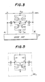
- FIG.3 shows an essential part of the second embodiment, that is, a memory cell part of an SRAM.
- those parts which are essentially the same as those corresponding parts in FIG.2 are designated by the same reference numerals, and a description thereof will be omitted.
- the memory cell part shown in FIG.3 includes four transistors Q1, Q2, Q5 and Q6, two capacitors C1 and C2, bit lines BL and BL , a main word line MWL and a sense amplifier SA which are coupled as shown.
- the main word line MWL is used in common as a positive power source line for supplying a positive power source voltage V DD .
- the transistors Q1 and Q2 are n-channel transistors, and the transistors Q5 and Q6 are p-channel transistors.
- the transistors Q1 and Q5 form a CMOS inverter, and the transistors Q2 and Q6 form another CMOS inverter.
- the transistors Q5 and Q6 are inserted in place of the resistors R1 and R2 shown in FIG.2.
- the data read/write is carried out similarly as in the first embodiment described above.
- a collection of such sub groups may be coupled to main bit lines by coupling the sub bit lines to the main bit lines via transfer gate transistors.
- the transfer gate transistors are driven by sub word lines.
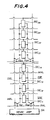
- FIG.4 shows an essential part of the third embodiment.
- the semiconductor memory device shown in FIG.4 includes memory cells MC11 through MC14, memory cells MC21 through MC24, main bit lines MBL and MBL , sub bit lines SBL and SBL , a sub word line SWL, and transfer gate transistors Q G1 through Q G4 which are connected as shown.
- FIG.5 shows a circuit structure of the memory cell MC11 shown in FIG.4.
- those parts which are the same as those corresponding parts in FIG.2 are designated by the same reference numerals, and a description thereof will be omitted.
- the other memory cells MC12 through MC14 and MC21 through MC24 have the same circuit structure.
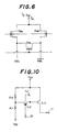
- FIG.6 shows an essential part of a bit line potential adjusting circuit which is not shown in FIG.4 but is coupled to the main bit lines MBL and MBL on an end opposite to the end where the sense amplifier SA is provided in FIG.4.
- a voltage V DD /2 is supplied to a terminal T BL
- the bit line potential adjusting circuit includes switching transistors Q BG for controlling the supply of voltage and a transistor Q BL for levelling the voltage.
- FIG.7A is a plan view showing an essential part of the third embodiment
- FIG.7B is a cross sectional view along a line A-A′ in FIG.7A.
- a description will now be given of a method of producing the third embodiment of the semiconductor memory device according to the present invention, by referring to FIGS.7A and 7B. This method generally is made up of steps (1) through (22).
- the semiconductor memory device is completed by the above described steps (1) through (22).
- the transistors Q1 and Q2 for holding data are MOS FETs, and for example, the channel length and the channel width of the MOS FET are 1 ⁇ m.
- the resistors R1 and R2 respectively are made of a non-doped or impurity doped polysilicon layer having a resistance of 100 M ⁇ , for example.
- the capacitors C1 and C2 respectively have a capacitance in the range of 5 fF to 10 fF.
- the capacitor C1 (or C2) which is used in place of the transfer gate transistor is formed between the gate electrode of the transistor Q1 (or Q2) and the bit line.
- the capacitor C1 (or C2) can be formed above the transistor Q1 (or Q2), and in the plan view of the semiconductor memory device the capacitor C1 (or C2) does not occupy an area exclusively therefor. For this reason, it is possible to improve the integration density of the semiconductor memory device, that is, the SRAM in this case.
- FIG.8(A) through 8(F) is a timing chart for explaining the read operation
- FIG.9(A) through 9(F) is a timing chart for explaining the write operation.
- T R1 denotes a time when a potential of the sub word line SWL is raised so as to couple the main bit lines MBL and MBL to the sub bit lines SBL and SBL
- T R2 denotes a time when the sense amplifier SA is operated.
- T W1 denotes a time when the main bit line MBL is set to a high level (or a low level) and the main bit line MBL is set to a low level (or a high level) depending on the write information
- T W2 denotes a time when the main bit lines MBL and MBL are short-circuited and set to an intermediate level
- T W3 denotes a time when the potential of the main word line MWL is raised to set a node A shown in FIG.5 to a high level and a node B shown in FIG.5 to a low level
- T W4 denotes a time when the main word line MWL is set to a low level so as to reduce the power consumption in a standby state.
- the power source voltage for the memory cells MC11, MC12, ..., that is, the potential of the main word line MWL is set to V DD /2. It is assumed that the level at the node A is set to the high level, and the level at the node B is set to the low level.
- the sub word line SWL is set to a high level to turn ON the transfer gate transistors Q G1 and Q G2 so as to select one group of memory cells MC11 through MC14.
- the main bit line MBL is connected to the sub bit line SBL
- the main bit line MBL is connected to the sub bit line SBL .
- the voltage applied to the main word line MWL that is, the power source voltage applied to the memory cell MC11, for example, is set to V DD so that the potential at the node A can be changed by V DD /2 virtually without changing the potential at the node B.
- the potential change at the node A is transmitted to the sub bit lines SBL and SBL via the respective capacitors C1 and C2 and is thus to the main bit lines MBL and MBL to change the potentials of the main bit lines MBL and MBL .
- the potential change of the main bit lines MBL and MBL can be detected by the sense amplifier SA.
- the sense amplifier SA may be operated in a state where the main bit lines MBL and MBL are disconnected.
- the power source voltage for the memory cells MC11, MC12, ..., that is, the potential of the main word line MWL is set to the ground potential.
- the main bit line MBL is set to a high level (or a low level) and the main bit line MBL is set to a low level (or a high level) depending on the write information which is to be written.
- the levelling transistor Q BL is turned ON to set the main bit lines MBL and MBL to the intermediate level.
- the potential at the node B slightly rises and the potential at the node A slightly falls.
- the potential of the main word line MWL is raised to set the node B to the high level (or low level) and the node A to the low level (or high level).
- the power source voltage for the memory cells MC11, MC12, ... that is, the potential of the main word line MWL is set to the ground potential.
- the main bit lines MBL and MBL are set to the intermediate level.
- the main bit line MBL is set to the high level (or low level) and the main bit line MBL is set to the low level (or high level) depending on the write information which is to be written.
- the potential of the main word line MWL is raised so as to set the node B (or A) to a high level.
- FIG.10 shows an essential part of an embodiment of a word line driving circuit.
- the word line driving circuit shown in FIG.10 includes a p-channel transistor Tr1, n-channel transistors Tr2 and Tr3, and resistors R10 and R11 which are connected as shown between a positive power source V DD and a negative power source V SS .
- a switching signal is applied to a terminal 10, and an output voltage from a terminal 11 is supplied to the main word line MWL (or MWL ) shown in FIG.4.
- the output voltage from the terminal 11 is V DD /2.
- the output voltage from the terminal 11 is V DD when the switching signal applied to the terminal 10 has a low level.
- FIG.11 shows an essential part of an embodiment of the sense amplifier SA
- FIG.12 is a timing chart for explaining the operation of the sense amplifier SA.
- the sense amplifier SA shown in FIG.11 generally includes transistors T1 through T9 which are connected as shown.
- ⁇ P denotes a precharge clock signal
- ⁇ SEN denotes a common source potential of the NMOS transistors T1 and T2
- ⁇ SEP denotes a common source potential of the PMOS transistors T3 and T4.
- ⁇ RW denotes a read/write clock signal for controlling the ON/OFF state of the transistors T8 and T9.
- the read/write clock signal ⁇ RW turns the transistors T8 and T9 ON and thereafter turns the transistors T8 and T9 OFF after the sense amplifier SA senses the potential difference across the bit lines BL and BL (or BLR and BLL).
- the sense amplifier SA senses the potential difference across the bit lines BL and BL (or BLR and BLL).
- a potential difference across bit lines BLR and BLL is amplified as shown in FIG.12.
- the read/write clock signal ⁇ RW controls the ON/OFF state of the transistors T8 and T9 as follows. That is, the transistors T8 and T9 are first turned OFF to set the potentials of the bit lines BL and BL to V DD /2 via the positive power source V DD . At the same time, the potential of the main word line MWL is lowered. Second, the transistors T8 and T9 are turned ON to latch the data to be written into the memory cell. Third, the transistors T8 and T9 are turned OFF, and at the same time, the potential of the main word line MWL is raised.
- FIG.13 a description will be given of a simulation which is carried out for the second embodiment.
- the simulation is carried out using a circuit structure shown in FIG.13.
- FIG.13 those parts which are the same as those corresponding parts in FIG.3 are designated by the same reference numerals, and a description thereof will be omitted.
- the main word line MWL is connected to a node N1, and this node N1 is coupled to the power source voltage V DD via a resistor R15 having a resistance of 2 k ⁇ .
- the capacitor C1 has a capacitance of 5 fF and is connected to the bit line BL at a node N4.
- This node N4 is coupled to a power source voltage V BB via a capacitor C11 having a capacitance of 50 fF.
- the capacitor C2 has a capacitance of 5 fF and is connected to the bit line BL at a node N5.
- This node N5 is coupled to a power source voltage V BB via a capacitor C12 having a capacitance of 50 fF.
- the transistors Q1 and Q5 and the capacitor C1 are connected at a node N2.
- the transistors Q2 and Q6 and the capacitor C2 are connected at a node N3.
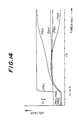
- FIG.14 is a timing chart for explaining the potentials at the nodes N1 through N5 in FIG.13 during a read operation.
- a potential PN1 at the node N1 is changed from 2 V to 6 V at a time t1
- potentials PN2 and PN3 at the respective nodes N2 and N3 change as shown.
- potentials PN4 and PN5 are obtained at the respective nodes N4 and N5.
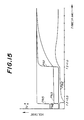
- FIG.15 is a timing chart for explaining the potentials at the nodes N1 through N5 in FIG.13 during a write operation.
- the potentials PN1 through PN3 are 0 V and the potentials PN4 and PN5 are 2 V.
- the potential PN4 is changed from 2 V to 0 V and the potential PN5 is changed from 2 V to 5 V at a time t2.
- the potential PN2 slightly rises and the potential PN3 slightly falls.
- the potential PN1 is changed from 0 V to 5 V. Consequently, the potential PN3 rises to 5 V and the potential PN2 falls to 0 V, and the write operation is completed.
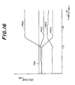
- FIG.16 is a timing chart for explaining the operation of the circuit shown in FIG.13. The same designations are used as in FIGS.14 and 15. It may be seen from FIG.16 that no data write operation is carried out with respect to those memory cells which are not selected. During the read operation, even when the sense amplifier SA amplifies the potential difference across the bit lines BL and BL , those memory cells which are not selected will not be inverted. On the other hand, during the read operation, even when the potentials of the pair of bit lines BL and BL are greatly changed, no data write operation takes place with respect to the memory cells which are also connected to the bit lines BL and BL but are other than the selected memory cell. For this reason, the data stored in the memory cells other than the selected memory cell will not be changed by the data write operation which is carried out with respect to the selected memory cell.
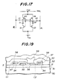
- FIG.17 is a circuit diagram showing an essential part of the fourth embodiment.
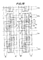
- FIG.18 is a plan view showing the fourth embodiment together with adjacent memory cells
- FIG.19 is a cross sectional view taken along a line B-B′ in FIG.18.
- FIGS.17 through 19 those parts which are essentially the same as those corresponding parts in FIGS.3, 7A and 7B are designated by the same reference numerals, and a description thereof will be omitted.
- a diode D1 is connected between the transistors Q1 and Q5
- a diode D2 is connected between the transistors Q2 and Q6.
- a SiO2 insulator layer 51 is formed on a substrate 50.
- a gate electrode layer 54 and Si regions 55 and 56 are formed on the SiO2 insulator layer 51.
- the Si region 55 corresponds to the source region of the transistor Q6, and the Si region 56 corresponds to the drain region of the transistor Q5.
- a SiO2 layer 57 and a WSi2 layer 58 are formed on the gate electrode layer 54.
- the SiO2 layer 51 is covered by an interlayer insulator 51.
- An Al contact layer 59 connects to the Si region 56.
- a covering layer 53 covers the substrate surface as shown.
- the WSi2 layer 58 shown on the left in FIG.19 corresponds to the bit line BL
- the WSi2 layer 58 shown on the right corresponds to the bit line BL.
- FIG.20 shows an essential part of the fifth embodiment, and in FIG.20, those parts which are the same as those corresponding parts in FIGS.2 through 4 are designated by the same reference numerals, and a description thereof will be omitted.
- the memory cells MC1 through MC3 are respectively connected to main word lines MWL1 through MWL3.
- the memory cells MC1 through MC3 have the same circuit structure, and the circuit structure shown in FIG.2, 3 or 17 may be used.
- a capacitor C is coupled to the bit line BL between the two adjacent memory cells MC1 and MC2 and between the two adjacent memory cells MC2 and MC3.
- a capacitor C is coupled to the bit line BL between the two adjacent memory cells MC1 and MC2 and between the two adjacent memory cells MC2 and MC3.
- the memory cell MC1 is used as a memory cell for storing information
- the memory cells MC2 and MC3 are used as transfer cells for transferring the information from the memory cell MC1 to the sense amplifier SA during the read operation and for transferring the information to the memory cell MC1 during the write operation.
- the transfer cells MC2 and MC3 substantially function as the bit lines. For this reason, it is possible to omit the transfer gate transistors shown in FIG.4, and also omit the bit line contacts.
- FIG.21(A) through (C) is a timing chart for explaining the read operation of this embodiment.
- the main word line MWL1 is set to V DD /2 which is 2.5 V in this embodiment, as shown in FIG.15(A).
- V DD which is 2.5 V in this embodiment
- the main word line MWL1 is set to V DD which is 5.0 V as shown in FIG.21(A).
- V DD which is 5.0 V as shown in FIG.21(A).
- the voltage at the node N11 is changed by V DD /2 substantially without changing the voltage at the node N12.
- This voltage change at the node N11 is transferred to the adjacent memory cell MC2 via the capacitor C and stored in the memory cell MC2 when the corresponding main word line MWL2 is set to V DD as shown in FIG.21(B).
- the information stored in the memory cell MC2 is transferred similarly to the memory cell MC3 and then supplied to the sense amplifier SA when the corresponding main word line MWL3 is set to V DD as shown in FIG.21(C).
- FIG.22(A) through (C) is a timing chart for explaining the write operation of this embodiment.
- the main word lines MWL1 through MWL3 are set to the ground level.
- the bit line BL at the sense amplifier SA is set to the high level (or low level) and the bit line BL at the sense amplifier SA is set to the low level (or high level).
- the main word lines MWL1, MWL2 and MWL3 are sequentially set to V DD as shown in FIG.22(A), (B) and (C), so as to transfer the information which is to be stored and finally store the information in the memory cell MC1.
Landscapes
- Engineering & Computer Science (AREA)
- Microelectronics & Electronic Packaging (AREA)
- Computer Hardware Design (AREA)
- Dram (AREA)
- Static Random-Access Memory (AREA)
- Semiconductor Memories (AREA)
Applications Claiming Priority (2)
| Application Number | Priority Date | Filing Date | Title |
|---|---|---|---|
| JP1252072A JPH03116488A (ja) | 1989-09-29 | 1989-09-29 | 半導体記憶装置 |
| JP252072/89 | 1989-09-29 |
Publications (2)
| Publication Number | Publication Date |
|---|---|
| EP0420646A2 true EP0420646A2 (de) | 1991-04-03 |
| EP0420646A3 EP0420646A3 (en) | 1992-03-18 |
Family
ID=17232162
Family Applications (1)
| Application Number | Title | Priority Date | Filing Date |
|---|---|---|---|
| EP19900310601 Ceased EP0420646A3 (en) | 1989-09-29 | 1990-09-27 | Semiconductor memory device having capacitor through which data read/write is carried out |
Country Status (4)
| Country | Link |
|---|---|
| US (1) | US5051952A (de) |
| EP (1) | EP0420646A3 (de) |
| JP (1) | JPH03116488A (de) |
| KR (1) | KR940004519B1 (de) |
Cited By (3)
| Publication number | Priority date | Publication date | Assignee | Title |
|---|---|---|---|---|
| EP0465170A3 (en) * | 1990-06-29 | 1992-07-29 | Sharp Kabushiki Kaisha | Static ram cell |
| US5210429A (en) * | 1990-06-29 | 1993-05-11 | Sharp Kabushiki Kaisha | Static RAM cell with conductive straps formed integrally with thin film transistor gates |
| EP0840325A3 (de) * | 1996-10-31 | 1999-06-09 | Texas Instruments Incorporated | Verbesserungen an oder bei Speicheranordnungen |
Families Citing this family (13)
| Publication number | Priority date | Publication date | Assignee | Title |
|---|---|---|---|---|
| JP2550207B2 (ja) * | 1990-06-08 | 1996-11-06 | 株式会社東芝 | 半導体メモリセル |
| JP2680939B2 (ja) * | 1991-03-27 | 1997-11-19 | 日本電気アイシーマイコンシステム株式会社 | 半導体記憶装置 |
| JPH04345992A (ja) * | 1991-05-24 | 1992-12-01 | Fujitsu Ltd | スタティックram |
| US5452246A (en) * | 1993-06-02 | 1995-09-19 | Fujitsu Limited | Static semiconductor memory device adapted for stabilization of low-voltage operation and reduction in cell size |
| TW335503B (en) * | 1996-02-23 | 1998-07-01 | Semiconductor Energy Lab Kk | Semiconductor thin film and manufacturing method and semiconductor device and its manufacturing method |
| US6046930A (en) * | 1998-09-01 | 2000-04-04 | International Business Machines Corporation | Memory array and method for writing data to memory |
| US6768348B2 (en) | 2001-11-30 | 2004-07-27 | Semiconductor Energy Laboratory Co., Ltd. | Sense amplifier and electronic apparatus using the same |
| JP4260469B2 (ja) * | 2002-12-16 | 2009-04-30 | 株式会社ルネサステクノロジ | 半導体記憶装置 |
| US7385841B2 (en) * | 2005-08-15 | 2008-06-10 | Texas Instruments Incorporated | Static random access memory device having a voltage-controlled word line driver for retain till accessed mode and method of operating the same |
| JP4907563B2 (ja) * | 2008-01-16 | 2012-03-28 | パナソニック株式会社 | 半導体記憶装置 |
| US9449667B2 (en) | 2014-03-31 | 2016-09-20 | Taiwan Semiconductor Manufacturing Company, Ltd. | Memory circuit having shared word line |
| KR102634434B1 (ko) * | 2018-12-24 | 2024-02-06 | 에스케이하이닉스 주식회사 | 반도체 메모리 장치 및 그 동작 방법 |
| JP2020202005A (ja) * | 2020-07-30 | 2020-12-17 | 株式会社半導体エネルギー研究所 | 半導体装置 |
Family Cites Families (8)
| Publication number | Priority date | Publication date | Assignee | Title |
|---|---|---|---|---|
| US3281630A (en) * | 1964-01-02 | 1966-10-25 | Ampex | Pulse width modulator for step motor |
| US3363115A (en) * | 1965-03-29 | 1968-01-09 | Gen Micro Electronics Inc | Integral counting circuit with storage capacitors in the conductive path of steering gate circuits |
| US3636527A (en) * | 1970-08-21 | 1972-01-18 | Rca Corp | Storage circuit |
| US3969708A (en) * | 1975-06-30 | 1976-07-13 | International Business Machines Corporation | Static four device memory cell |
| US4032902A (en) * | 1975-10-30 | 1977-06-28 | Fairchild Camera And Instrument Corporation | An improved semiconductor memory cell circuit and structure |
| US4719600A (en) * | 1986-02-18 | 1988-01-12 | International Business Machines Corporation | Sense circuit for multilevel storage system |
| JPS62273694A (ja) * | 1986-05-22 | 1987-11-27 | Sony Corp | センスアンプ |
| EP0523756A3 (en) * | 1986-08-15 | 1993-06-09 | Nec Corporation | Static random access memory having bi-cmos construction |
-
1989
- 1989-09-29 JP JP1252072A patent/JPH03116488A/ja active Pending
-
1990
- 1990-09-25 US US07/588,629 patent/US5051952A/en not_active Expired - Lifetime
- 1990-09-27 EP EP19900310601 patent/EP0420646A3/en not_active Ceased
- 1990-09-28 KR KR1019900015437A patent/KR940004519B1/ko not_active Expired - Fee Related
Cited By (3)
| Publication number | Priority date | Publication date | Assignee | Title |
|---|---|---|---|---|
| EP0465170A3 (en) * | 1990-06-29 | 1992-07-29 | Sharp Kabushiki Kaisha | Static ram cell |
| US5210429A (en) * | 1990-06-29 | 1993-05-11 | Sharp Kabushiki Kaisha | Static RAM cell with conductive straps formed integrally with thin film transistor gates |
| EP0840325A3 (de) * | 1996-10-31 | 1999-06-09 | Texas Instruments Incorporated | Verbesserungen an oder bei Speicheranordnungen |
Also Published As
| Publication number | Publication date |
|---|---|
| EP0420646A3 (en) | 1992-03-18 |
| US5051952A (en) | 1991-09-24 |
| KR940004519B1 (ko) | 1994-05-25 |
| KR910006991A (ko) | 1991-04-30 |
| JPH03116488A (ja) | 1991-05-17 |
Similar Documents
| Publication | Publication Date | Title |
|---|---|---|
| US7978560B2 (en) | Static memory cell having independent data holding voltage | |
| EP0420646A2 (de) | Halbleiterspeicheranordnung mit Kondensator durch den ein Lesen/Schreiben von Daten durchgeführt wird | |
| JP3467416B2 (ja) | 半導体記憶装置及びその製造方法 | |
| US4799197A (en) | Semiconductor memory device having a CMOS sense amplifier | |
| US6801449B2 (en) | Semiconductor memory device | |
| US6306704B1 (en) | Nonvolatile ferroelectric memory | |
| KR100460578B1 (ko) | 로드없는 4-트랜지스터 메모리셀 | |
| US5267192A (en) | Semiconductor memory device | |
| US6115309A (en) | Sense amplifier having increased drive current capability | |
| JPH0369092A (ja) | ダイナミックram用メモリセル回路 | |
| EP0691685B1 (de) | SRAM-Anordnung mit Last-Dünnschichttransistoren | |
| US5491654A (en) | Static random access memory device having thin film transistor loads | |
| JPH0917965A (ja) | 半導体集積回路装置およびその製造方法 | |
| JPH10162589A (ja) | 強誘電体メモリ装置 | |
| US20010011739A1 (en) | Ferroelectric random access memory device | |
| EP0740304A2 (de) | Ferroelektrischer Speicher mit fester Mittelbereichsspannung an der Plattenelektrode | |
| JPS60256998A (ja) | ダイナミツク型半導体記憶装置 | |
| KR940000892B1 (ko) | 다미나믹 ram용 메모리셀회로 | |
| JPH0621395A (ja) | 半導体記憶装置及びその製造方法 | |
| JPS60258796A (ja) | ダイナミツク型半導体記憶装置 |
Legal Events
| Date | Code | Title | Description |
|---|---|---|---|
| PUAI | Public reference made under article 153(3) epc to a published international application that has entered the european phase |
Free format text: ORIGINAL CODE: 0009012 |
|
| AK | Designated contracting states |
Kind code of ref document: A2 Designated state(s): DE FR GB |
|
| PUAL | Search report despatched |
Free format text: ORIGINAL CODE: 0009013 |
|
| AK | Designated contracting states |
Kind code of ref document: A3 Designated state(s): DE FR GB |
|
| 17P | Request for examination filed |
Effective date: 19920421 |
|
| 17Q | First examination report despatched |
Effective date: 19940527 |
|
| STAA | Information on the status of an ep patent application or granted ep patent |
Free format text: STATUS: THE APPLICATION HAS BEEN REFUSED |
|
| 18R | Application refused |
Effective date: 19951008 |