EP0420597A2 - Verfahren zur Herstellung einer abgeschiedenen Schicht unter Verwendung von Alkylaluminiumhydrid und Verfahren zur Herstellung eines Halbleiterbauelements - Google Patents
Verfahren zur Herstellung einer abgeschiedenen Schicht unter Verwendung von Alkylaluminiumhydrid und Verfahren zur Herstellung eines Halbleiterbauelements Download PDFInfo
- Publication number
- EP0420597A2 EP0420597A2 EP90310508A EP90310508A EP0420597A2 EP 0420597 A2 EP0420597 A2 EP 0420597A2 EP 90310508 A EP90310508 A EP 90310508A EP 90310508 A EP90310508 A EP 90310508A EP 0420597 A2 EP0420597 A2 EP 0420597A2
- Authority
- EP
- European Patent Office
- Prior art keywords
- film
- deposition
- deposited
- substrate
- torr
- Prior art date
- Legal status (The legal status is an assumption and is not a legal conclusion. Google has not performed a legal analysis and makes no representation as to the accuracy of the status listed.)
- Granted
Links
- 238000000034 method Methods 0.000 title claims abstract description 120
- 125000005234 alkyl aluminium group Chemical group 0.000 title claims abstract description 30
- 230000008569 process Effects 0.000 title claims description 24
- 239000004065 semiconductor Substances 0.000 title claims description 24
- 238000004519 manufacturing process Methods 0.000 title claims description 5
- 238000000151 deposition Methods 0.000 claims abstract description 343
- 230000008021 deposition Effects 0.000 claims abstract description 329
- 239000007789 gas Substances 0.000 claims abstract description 129
- 230000015572 biosynthetic process Effects 0.000 claims abstract description 73
- UFHFLCQGNIYNRP-UHFFFAOYSA-N Hydrogen Chemical compound [H][H] UFHFLCQGNIYNRP-UHFFFAOYSA-N 0.000 claims abstract description 17
- 239000000758 substrate Substances 0.000 claims description 337
- CSDREXVUYHZDNP-UHFFFAOYSA-N alumanylidynesilicon Chemical compound [Al].[Si] CSDREXVUYHZDNP-UHFFFAOYSA-N 0.000 claims description 185
- TUTOKIOKAWTABR-UHFFFAOYSA-N dimethylalumane Chemical group C[AlH]C TUTOKIOKAWTABR-UHFFFAOYSA-N 0.000 claims description 137
- 229910052782 aluminium Inorganic materials 0.000 claims description 62
- 229910052751 metal Inorganic materials 0.000 claims description 46
- 239000002184 metal Substances 0.000 claims description 46
- XAGFODPZIPBFFR-UHFFFAOYSA-N aluminium Chemical compound [Al] XAGFODPZIPBFFR-UHFFFAOYSA-N 0.000 claims description 23
- 238000000354 decomposition reaction Methods 0.000 claims description 17
- 229910052710 silicon Inorganic materials 0.000 claims description 15
- 239000010703 silicon Substances 0.000 claims description 14
- 229910052739 hydrogen Inorganic materials 0.000 claims description 6
- 239000001257 hydrogen Substances 0.000 claims description 6
- CWEHKOAQFGHCFQ-UHFFFAOYSA-N methylalumane Chemical group [AlH2]C CWEHKOAQFGHCFQ-UHFFFAOYSA-N 0.000 claims description 3
- AZDRQVAHHNSJOQ-UHFFFAOYSA-N alumane Chemical compound [AlH3] AZDRQVAHHNSJOQ-UHFFFAOYSA-N 0.000 claims 1
- 238000005229 chemical vapour deposition Methods 0.000 abstract description 33
- 239000010408 film Substances 0.000 description 383
- 238000006243 chemical reaction Methods 0.000 description 93
- VYPSYNLAJGMNEJ-UHFFFAOYSA-N Silicium dioxide Chemical compound O=[Si]=O VYPSYNLAJGMNEJ-UHFFFAOYSA-N 0.000 description 83
- 235000012431 wafers Nutrition 0.000 description 78
- 229910007264 Si2H6 Inorganic materials 0.000 description 53
- PZPGRFITIJYNEJ-UHFFFAOYSA-N disilane Chemical compound [SiH3][SiH3] PZPGRFITIJYNEJ-UHFFFAOYSA-N 0.000 description 53
- 229910052681 coesite Inorganic materials 0.000 description 42
- 229910052906 cristobalite Inorganic materials 0.000 description 42
- 239000000377 silicon dioxide Substances 0.000 description 42
- 229910052682 stishovite Inorganic materials 0.000 description 42
- 229910052905 tridymite Inorganic materials 0.000 description 42
- 235000012239 silicon dioxide Nutrition 0.000 description 41
- 239000000463 material Substances 0.000 description 37
- 229910021421 monocrystalline silicon Inorganic materials 0.000 description 28
- 238000002128 reflection high energy electron diffraction Methods 0.000 description 22
- 229910052799 carbon Inorganic materials 0.000 description 20
- 239000012159 carrier gas Substances 0.000 description 20
- 238000010894 electron beam technology Methods 0.000 description 20
- 238000002441 X-ray diffraction Methods 0.000 description 18
- 238000004518 low pressure chemical vapour deposition Methods 0.000 description 18
- 239000010409 thin film Substances 0.000 description 17
- 239000013078 crystal Substances 0.000 description 16
- 238000010438 heat treatment Methods 0.000 description 15
- -1 Al-Si compound Chemical class 0.000 description 11
- 230000006872 improvement Effects 0.000 description 11
- 229910021420 polycrystalline silicon Inorganic materials 0.000 description 11
- OKTJSMMVPCPJKN-UHFFFAOYSA-N Carbon Chemical compound [C] OKTJSMMVPCPJKN-UHFFFAOYSA-N 0.000 description 10
- IEQUNHXCJVILJQ-UHFFFAOYSA-N aluminum palladium Chemical compound [Al].[Pd] IEQUNHXCJVILJQ-UHFFFAOYSA-N 0.000 description 10
- 125000004429 atom Chemical group 0.000 description 10
- YXTPWUNVHCYOSP-UHFFFAOYSA-N bis($l^{2}-silanylidene)molybdenum Chemical compound [Si]=[Mo]=[Si] YXTPWUNVHCYOSP-UHFFFAOYSA-N 0.000 description 10
- 239000010949 copper Substances 0.000 description 10
- 238000011156 evaluation Methods 0.000 description 10
- 239000000203 mixture Substances 0.000 description 10
- 239000012495 reaction gas Substances 0.000 description 10
- 229910052715 tantalum Inorganic materials 0.000 description 10
- GUVRBAGPIYLISA-UHFFFAOYSA-N tantalum atom Chemical compound [Ta] GUVRBAGPIYLISA-UHFFFAOYSA-N 0.000 description 10
- XUIMIQQOPSSXEZ-UHFFFAOYSA-N Silicon Chemical compound [Si] XUIMIQQOPSSXEZ-UHFFFAOYSA-N 0.000 description 9
- 229910021417 amorphous silicon Inorganic materials 0.000 description 9
- 230000001965 increasing effect Effects 0.000 description 9
- 125000002496 methyl group Chemical group [H]C([H])([H])* 0.000 description 9
- 229910021344 molybdenum silicide Inorganic materials 0.000 description 9
- 238000000059 patterning Methods 0.000 description 9
- 239000010936 titanium Substances 0.000 description 9
- NRTOMJZYCJJWKI-UHFFFAOYSA-N Titanium nitride Chemical compound [Ti]#N NRTOMJZYCJJWKI-UHFFFAOYSA-N 0.000 description 8
- 230000000694 effects Effects 0.000 description 8
- 229910052698 phosphorus Inorganic materials 0.000 description 8
- OAICVXFJPJFONN-UHFFFAOYSA-N Phosphorus Chemical compound [P] OAICVXFJPJFONN-UHFFFAOYSA-N 0.000 description 7
- 230000001276 controlling effect Effects 0.000 description 7
- 150000002739 metals Chemical class 0.000 description 7
- 239000011574 phosphorus Substances 0.000 description 7
- 238000004544 sputter deposition Methods 0.000 description 7
- JLTRXTDYQLMHGR-UHFFFAOYSA-N trimethylaluminium Chemical compound C[Al](C)C JLTRXTDYQLMHGR-UHFFFAOYSA-N 0.000 description 7
- 239000012535 impurity Substances 0.000 description 6
- 238000013508 migration Methods 0.000 description 6
- 238000005268 plasma chemical vapour deposition Methods 0.000 description 6
- 229910021332 silicide Inorganic materials 0.000 description 6
- ZOXJGFHDIHLPTG-UHFFFAOYSA-N Boron Chemical compound [B] ZOXJGFHDIHLPTG-UHFFFAOYSA-N 0.000 description 5
- RYGMFSIKBFXOCR-UHFFFAOYSA-N Copper Chemical compound [Cu] RYGMFSIKBFXOCR-UHFFFAOYSA-N 0.000 description 5
- ZOKXTWBITQBERF-UHFFFAOYSA-N Molybdenum Chemical compound [Mo] ZOKXTWBITQBERF-UHFFFAOYSA-N 0.000 description 5
- BLRPTPMANUNPDV-UHFFFAOYSA-N Silane Chemical compound [SiH4] BLRPTPMANUNPDV-UHFFFAOYSA-N 0.000 description 5
- RTAQQCXQSZGOHL-UHFFFAOYSA-N Titanium Chemical compound [Ti] RTAQQCXQSZGOHL-UHFFFAOYSA-N 0.000 description 5
- UGACIEPFGXRWCH-UHFFFAOYSA-N [Si].[Ti] Chemical compound [Si].[Ti] UGACIEPFGXRWCH-UHFFFAOYSA-N 0.000 description 5
- 230000001133 acceleration Effects 0.000 description 5
- 125000000217 alkyl group Chemical group 0.000 description 5
- UQZIWOQVLUASCR-UHFFFAOYSA-N alumane;titanium Chemical compound [AlH3].[Ti] UQZIWOQVLUASCR-UHFFFAOYSA-N 0.000 description 5
- 229910052796 boron Inorganic materials 0.000 description 5
- 230000008859 change Effects 0.000 description 5
- 229910052802 copper Inorganic materials 0.000 description 5
- 230000000875 corresponding effect Effects 0.000 description 5
- 230000005012 migration Effects 0.000 description 5
- 229910052750 molybdenum Inorganic materials 0.000 description 5
- 239000011733 molybdenum Substances 0.000 description 5
- 230000003647 oxidation Effects 0.000 description 5
- 238000007254 oxidation reaction Methods 0.000 description 5
- FVBUAEGBCNSCDD-UHFFFAOYSA-N silicide(4-) Chemical compound [Si-4] FVBUAEGBCNSCDD-UHFFFAOYSA-N 0.000 description 5
- WNUPENMBHHEARK-UHFFFAOYSA-N silicon tungsten Chemical compound [Si].[W] WNUPENMBHHEARK-UHFFFAOYSA-N 0.000 description 5
- 229910052719 titanium Inorganic materials 0.000 description 5
- WFKWXMTUELFFGS-UHFFFAOYSA-N tungsten Chemical compound [W] WFKWXMTUELFFGS-UHFFFAOYSA-N 0.000 description 5
- 229910052721 tungsten Inorganic materials 0.000 description 5
- 239000010937 tungsten Substances 0.000 description 5
- 229910018594 Si-Cu Inorganic materials 0.000 description 4
- 229910008465 Si—Cu Inorganic materials 0.000 description 4
- 230000009471 action Effects 0.000 description 4
- 239000005380 borophosphosilicate glass Substances 0.000 description 4
- 150000001875 compounds Chemical class 0.000 description 4
- 230000006378 damage Effects 0.000 description 4
- 125000004435 hydrogen atom Chemical group [H]* 0.000 description 4
- 239000002245 particle Substances 0.000 description 4
- 229920002120 photoresistant polymer Polymers 0.000 description 4
- 238000001020 plasma etching Methods 0.000 description 4
- 238000002360 preparation method Methods 0.000 description 4
- 239000010453 quartz Substances 0.000 description 4
- 230000009467 reduction Effects 0.000 description 4
- 238000006557 surface reaction Methods 0.000 description 4
- 238000005979 thermal decomposition reaction Methods 0.000 description 4
- 238000005406 washing Methods 0.000 description 4
- 229910003074 TiCl4 Inorganic materials 0.000 description 3
- 230000002939 deleterious effect Effects 0.000 description 3
- 125000001495 ethyl group Chemical group [H]C([H])([H])C([H])([H])* 0.000 description 3
- 239000003574 free electron Substances 0.000 description 3
- 230000010354 integration Effects 0.000 description 3
- 239000007788 liquid Substances 0.000 description 3
- 230000007246 mechanism Effects 0.000 description 3
- 230000003287 optical effect Effects 0.000 description 3
- 238000002230 thermal chemical vapour deposition Methods 0.000 description 3
- XJDNKRIXUMDJCW-UHFFFAOYSA-J titanium tetrachloride Chemical compound Cl[Ti](Cl)(Cl)Cl XJDNKRIXUMDJCW-UHFFFAOYSA-J 0.000 description 3
- VOITXYVAKOUIBA-UHFFFAOYSA-N triethylaluminium Chemical compound CC[Al](CC)CC VOITXYVAKOUIBA-UHFFFAOYSA-N 0.000 description 3
- MCULRUJILOGHCJ-UHFFFAOYSA-N triisobutylaluminium Chemical compound CC(C)C[Al](CC(C)C)CC(C)C MCULRUJILOGHCJ-UHFFFAOYSA-N 0.000 description 3
- 229910045601 alloy Inorganic materials 0.000 description 2
- 239000000956 alloy Substances 0.000 description 2
- 238000004458 analytical method Methods 0.000 description 2
- QVGXLLKOCUKJST-UHFFFAOYSA-N atomic oxygen Chemical compound [O] QVGXLLKOCUKJST-UHFFFAOYSA-N 0.000 description 2
- 238000007068 beta-elimination reaction Methods 0.000 description 2
- 238000002485 combustion reaction Methods 0.000 description 2
- 239000000470 constituent Substances 0.000 description 2
- 238000011109 contamination Methods 0.000 description 2
- 238000011161 development Methods 0.000 description 2
- 238000002050 diffraction method Methods 0.000 description 2
- 238000009792 diffusion process Methods 0.000 description 2
- 239000000539 dimer Substances 0.000 description 2
- 238000001941 electron spectroscopy Methods 0.000 description 2
- 230000003028 elevating effect Effects 0.000 description 2
- 238000005530 etching Methods 0.000 description 2
- 229910052733 gallium Inorganic materials 0.000 description 2
- 238000009413 insulation Methods 0.000 description 2
- 229910052760 oxygen Inorganic materials 0.000 description 2
- 239000001301 oxygen Substances 0.000 description 2
- 239000007787 solid Substances 0.000 description 2
- 238000004611 spectroscopical analysis Methods 0.000 description 2
- 239000000126 substance Substances 0.000 description 2
- 238000000427 thin-film deposition Methods 0.000 description 2
- RFONJRMUUALMBA-UHFFFAOYSA-N 2-methanidylpropane Chemical compound CC(C)[CH2-] RFONJRMUUALMBA-UHFFFAOYSA-N 0.000 description 1
- 229910000838 Al alloy Inorganic materials 0.000 description 1
- 229910007159 Si(CH3)4 Inorganic materials 0.000 description 1
- 229910005096 Si3H8 Inorganic materials 0.000 description 1
- 229910003910 SiCl4 Inorganic materials 0.000 description 1
- 229910003818 SiH2Cl2 Inorganic materials 0.000 description 1
- 229910003826 SiH3Cl Inorganic materials 0.000 description 1
- LKTZODAHLMBGLG-UHFFFAOYSA-N alumanylidynesilicon;$l^{2}-alumanylidenesilylidenealuminum Chemical compound [Si]#[Al].[Si]#[Al].[Al]=[Si]=[Al] LKTZODAHLMBGLG-UHFFFAOYSA-N 0.000 description 1
- WPPDFTBPZNZZRP-UHFFFAOYSA-N aluminum copper Chemical compound [Al].[Cu] WPPDFTBPZNZZRP-UHFFFAOYSA-N 0.000 description 1
- LNGCCWNRTBPYAG-UHFFFAOYSA-N aluminum tantalum Chemical compound [Al].[Ta] LNGCCWNRTBPYAG-UHFFFAOYSA-N 0.000 description 1
- 229910052785 arsenic Inorganic materials 0.000 description 1
- 229910002056 binary alloy Inorganic materials 0.000 description 1
- 238000012769 bulk production Methods 0.000 description 1
- 125000004432 carbon atom Chemical group C* 0.000 description 1
- SLLGVCUQYRMELA-UHFFFAOYSA-N chlorosilicon Chemical compound Cl[Si] SLLGVCUQYRMELA-UHFFFAOYSA-N 0.000 description 1
- 238000003776 cleavage reaction Methods 0.000 description 1
- 230000000052 comparative effect Effects 0.000 description 1
- 230000002950 deficient Effects 0.000 description 1
- 238000005137 deposition process Methods 0.000 description 1
- 230000006866 deterioration Effects 0.000 description 1
- 230000005284 excitation Effects 0.000 description 1
- 238000002309 gasification Methods 0.000 description 1
- 239000011521 glass Substances 0.000 description 1
- 229910021478 group 5 element Inorganic materials 0.000 description 1
- 230000020169 heat generation Effects 0.000 description 1
- 229910052738 indium Inorganic materials 0.000 description 1
- 239000011261 inert gas Substances 0.000 description 1
- 239000011810 insulating material Substances 0.000 description 1
- 150000002500 ions Chemical class 0.000 description 1
- 238000001755 magnetron sputter deposition Methods 0.000 description 1
- 230000004048 modification Effects 0.000 description 1
- 238000012986 modification Methods 0.000 description 1
- 229910052757 nitrogen Inorganic materials 0.000 description 1
- 238000005289 physical deposition Methods 0.000 description 1
- 238000000197 pyrolysis Methods 0.000 description 1
- 229910002059 quaternary alloy Inorganic materials 0.000 description 1
- 238000007788 roughening Methods 0.000 description 1
- 229920006395 saturated elastomer Polymers 0.000 description 1
- 230000007017 scission Effects 0.000 description 1
- FDNAPBUWERUEDA-UHFFFAOYSA-N silicon tetrachloride Chemical compound Cl[Si](Cl)(Cl)Cl FDNAPBUWERUEDA-UHFFFAOYSA-N 0.000 description 1
- 238000000992 sputter etching Methods 0.000 description 1
- 239000007858 starting material Substances 0.000 description 1
- 125000001424 substituent group Chemical group 0.000 description 1
- CZDYPVPMEAXLPK-UHFFFAOYSA-N tetramethylsilane Chemical compound C[Si](C)(C)C CZDYPVPMEAXLPK-UHFFFAOYSA-N 0.000 description 1
- 229910021341 titanium silicide Inorganic materials 0.000 description 1
- RGGPNXQUMRMPRA-UHFFFAOYSA-N triethylgallium Chemical compound CC[Ga](CC)CC RGGPNXQUMRMPRA-UHFFFAOYSA-N 0.000 description 1
- XCZXGTMEAKBVPV-UHFFFAOYSA-N trimethylgallium Chemical compound C[Ga](C)C XCZXGTMEAKBVPV-UHFFFAOYSA-N 0.000 description 1
- WQJQOUPTWCFRMM-UHFFFAOYSA-N tungsten disilicide Chemical compound [Si]#[W]#[Si] WQJQOUPTWCFRMM-UHFFFAOYSA-N 0.000 description 1
- 229910021342 tungsten silicide Inorganic materials 0.000 description 1
Images


Classifications
-
- H—ELECTRICITY
- H01—ELECTRIC ELEMENTS
- H01L—SEMICONDUCTOR DEVICES NOT COVERED BY CLASS H10
- H01L21/00—Processes or apparatus adapted for the manufacture or treatment of semiconductor or solid state devices or of parts thereof
- H01L21/02—Manufacture or treatment of semiconductor devices or of parts thereof
- H01L21/04—Manufacture or treatment of semiconductor devices or of parts thereof the devices having potential barriers, e.g. a PN junction, depletion layer or carrier concentration layer
- H01L21/18—Manufacture or treatment of semiconductor devices or of parts thereof the devices having potential barriers, e.g. a PN junction, depletion layer or carrier concentration layer the devices having semiconductor bodies comprising elements of Group IV of the Periodic Table or AIIIBV compounds with or without impurities, e.g. doping materials
- H01L21/20—Deposition of semiconductor materials on a substrate, e.g. epitaxial growth solid phase epitaxy
-
- H—ELECTRICITY
- H01—ELECTRIC ELEMENTS
- H01L—SEMICONDUCTOR DEVICES NOT COVERED BY CLASS H10
- H01L21/00—Processes or apparatus adapted for the manufacture or treatment of semiconductor or solid state devices or of parts thereof
- H01L21/02—Manufacture or treatment of semiconductor devices or of parts thereof
- H01L21/04—Manufacture or treatment of semiconductor devices or of parts thereof the devices having potential barriers, e.g. a PN junction, depletion layer or carrier concentration layer
- H01L21/18—Manufacture or treatment of semiconductor devices or of parts thereof the devices having potential barriers, e.g. a PN junction, depletion layer or carrier concentration layer the devices having semiconductor bodies comprising elements of Group IV of the Periodic Table or AIIIBV compounds with or without impurities, e.g. doping materials
- H01L21/28—Manufacture of electrodes on semiconductor bodies using processes or apparatus not provided for in groups H01L21/20 - H01L21/268
- H01L21/283—Deposition of conductive or insulating materials for electrodes conducting electric current
- H01L21/285—Deposition of conductive or insulating materials for electrodes conducting electric current from a gas or vapour, e.g. condensation
- H01L21/28506—Deposition of conductive or insulating materials for electrodes conducting electric current from a gas or vapour, e.g. condensation of conductive layers
- H01L21/28512—Deposition of conductive or insulating materials for electrodes conducting electric current from a gas or vapour, e.g. condensation of conductive layers on semiconductor bodies comprising elements of Group IV of the Periodic Table
- H01L21/28556—Deposition of conductive or insulating materials for electrodes conducting electric current from a gas or vapour, e.g. condensation of conductive layers on semiconductor bodies comprising elements of Group IV of the Periodic Table by chemical means, e.g. CVD, LPCVD, PECVD, laser CVD
- H01L21/28562—Selective deposition
-
- H—ELECTRICITY
- H01—ELECTRIC ELEMENTS
- H01L—SEMICONDUCTOR DEVICES NOT COVERED BY CLASS H10
- H01L21/00—Processes or apparatus adapted for the manufacture or treatment of semiconductor or solid state devices or of parts thereof
- H01L21/70—Manufacture or treatment of devices consisting of a plurality of solid state components formed in or on a common substrate or of parts thereof; Manufacture of integrated circuit devices or of parts thereof
- H01L21/71—Manufacture of specific parts of devices defined in group H01L21/70
- H01L21/768—Applying interconnections to be used for carrying current between separate components within a device comprising conductors and dielectrics
- H01L21/76838—Applying interconnections to be used for carrying current between separate components within a device comprising conductors and dielectrics characterised by the formation and the after-treatment of the conductors
- H01L21/76877—Filling of holes, grooves or trenches, e.g. vias, with conductive material
- H01L21/76879—Filling of holes, grooves or trenches, e.g. vias, with conductive material by selective deposition of conductive material in the vias, e.g. selective C.V.D. on semiconductor material, plating
Definitions
- This invention relates to a process for forming a deposited film, particularly a process for forming a deposited film composed mainly of Al which can be preferably applied to electrodes or wiring of a semiconductor integrated circuit device, etc. and to a process for preparing a semiconductor device.
- Al aluminum
- Al-Si aluminum
- Al-Si aluminum
- Al has many advantages such that it is inexpensive and high in electroconductivity, that it can be also internally chemically protected because a dense oxidized film can be formed on the surface, and that it has good adhesion to Si, etc.
- the sputtering is the physical deposition method based on flying of sputtered particles in vacuum, the film thickness at the stepped portion or the insulating film side wall becomes extremely thin, leading to wire breaking in an extreme case.
- Nonuniformity of film thickness or wire breaking has the drawback that reliability of LSI is markedly lowered.
- the aspect ratio (via-hole depth/via-hole diameter) of via-hole in which a metal composed mainly of Al such as Al-Si, etc. is to be deposited is 1.0 or more, and the via-hole diameter itself also becomes 1 ⁇ m or less. Therefore, even for a via-hole with large aspect ratio, the technique which can deposit an Al-Si compound is required.
- Al-Si is required to be deposited so as to embed only the via-hole of the device.
- a method of depositing an Al alloy only on Si or metal surface and not depositing it on an insulating film such as SiO2, etc. is required.
- the bias sputtering method in which a bias is applied on a substrate and deposition is performed so as to embed Al or an Al-Si compound only in the via-hole by utilizing the sputter etching action and the deposition action on the substrate surface.
- the bias voltage of some 100 V or higher is applied on the substrate, deleterious influence on the device occurs because of charged particle damaging such as change in threshold of MOSFET, etc.
- the deposition speed cannot be essentially improved.
- CVD Chemical Vapor Deposition
- plasma CVD or optical CVD decomposition of the starting gas occurs in gas phase, and the active species formed there further reacts on the substrate to give rise to film formation.
- surface coverage on unevenness on the substrate surface is good.
- carbon atoms contained in the starting gas molecule are incorporated into the film.
- plasma CVD the problem remained that there was damage by charged particles (so called plasma damage) as in the case of the sputtering method.
- the thermal CVD method in which the film grows through the surface reaction primarily on the substrate surface, is good in surface coverage on unevenness such as stepped portion of the surface, etc. Also, it can be expected that deposition within via-hole will readily occur. Further, wire breaking at the stepped portion can be avoided. Furthermore, there are not caused damages by charged particles which have been observed in the case of the plasma CVD or the sputtering method.
- the methods of such a kind include, for example, the method seen in Journal of Electrochemical Society, Vol. 131, p. 2175 (1984).
- triisobutyl aluminum (i-C4H9)3Al (TIBA) is used as organic aluminum gas and an Al film is formed at a film formation temperature of 260 o C and a reaction tube pressure of 0.5 Torr.
- the substrate temperature is then maintained at about 450°C and SiH4 is introduced to diffuse Si in the Al film, thus obtaining an Al-Si film.
- TIBA When TIBA is to be used, a continuous film can not be obtained unless pretreatment is effected in which prior to film formation, TiCl4 is flowed to activate the substrate surface to form nuclei. Furthermore, in case where TIBA is used, there is a problem that surface flatness is not sufficient even when TiCl4 is used. By this method it is not possible to effect selective growth such as Al-Si deposition only in via-holes.
- Japanese Laid-Open Patent Application No. 63-33569 describes a method of forming a film by using no TiCl4, but using in place thereof organic aluminum and heating it in the vicinity of the substrate. According to this method, Al can be deposited selectively only on the metal or semiconductor surface from which the naturally oxidized film has been removed.
- the prior art methods have the problems to be solved that it is difficult to obtain a flat Al-Si film of a low resistivity and good quality, that there is considerable limitation in apparatus and in film formation.
- An object of the present invention is to provide a deposited film formation method which is, excellent in controllability, requires particularly no expensive and complicated deposited film formation device, is extremely wide in general purpose applicability, and yet can form a metal film of quality, and a method for producing a semiconductor device.
- An object of the present invention is to provide a deposited film formation method capable of forming a metal film composed mainly of Al of good quality according to the method excellent in reproducibility.
- Another object of the present invention is to provide a method for preparing a semiconductor device, which can provide a highly integrated semiconductor device of high performance at low cost.
- Another object of the present invention is to provide a deposited film formation method capable of forming a metal film composed mainly of Al of good quality at high deposition rate with excellent reproducibility at low cost.
- Still another object of the present invention is to provide a method for preparing a semiconductor device, which can obtain a wiring of good quality at high through-put and is high in reliability.
- Still another object of the present invention is to provide a deposited film formation method which can obtain a metal film composed mainly of Al of good quality at high deposition rate and with excellent selectivity, as well as a method for preparing a semiconductor device.
- Al or Al-Si film is formed by feeding a gas of an alkyl aluminum hydride, or a gas of an alkyl aluminum hydride together with a gas containing silicon.
- the deposition rate of Al is shifted during film formation. Accordingly, a dense Al or Al-Si film can be formed on a substrate at high speed.
- Al or Al-Si film is formed only on the electron donative surface (A), shifting the deposition rate of Al during film formation. Accordingly, a dense Al or Al-Si film can be formed at high speed only on the electron donative surface (A) on the substrate.
- the decomposition reaction of an organic metal and hence the thin film deposition reaction will vary greatly depending on the kind of the metal atom, the kind of the alkyl bonded to the metal atom, the means of causing the decomposition reaction to occur, the atmospheric gas, etc.
- trimethyl gallium: in thermal decomposition undergoes radical cleavage wherein Ga-CH3 bond is cleaved
- triethyl gallium: in thermal decomposition is decomposed through ⁇ -elimination into: and C2H4.
- triethyl aluminum attached with the same ethyl group: in thermal decomposition undergoes radical decomposition in which Al-C2H5 is cleaved.
- tri-iso-butyl aluminum having iC4H9 bonded therein: is subject to ⁇ -elimination.
- Trimethyl aluminum (TMA) comprising CH3 groups and Al has a dimer structure at room temperature: and thermal decomposition is radical decomposition in which Al-CH3 group is cleaved, and at a temperature of 150 o C or lower, it reacts with atmospheric H2 to form CH4, and forms finally Al.
- C2H6 will be formed by the bridging CH3 between two Al's.
- the excitation decomposition means for deposition of a metal atom from an organic metal on a desired substrate
- the decomposition reaction must be strictly controlled.
- Al is to be deposited from triisobutyl aluminum: in the low pressure CVD method comprising mainly thermal reaction, unevenness of ⁇ m order is formed on the surface, whereby the surface morphology is inferior.
- hillock generation by heat treatment, Si surface roughening through Si diffusion at the interface between Al and Si occur, and also migration resistance is inferior, whereby it can be utilized for ultra-LSI process with difficulty.
- the device is complicated, and the method is of the sheet treatment type in which deposition can be effected only on one wafer by one deposition process. Besides, since the deposition speed is 500 ⁇ /min. at the highest, the throughput necessary for bulk production cannot be realized.
- Dimethyl aluminum hydride (DMAH) as the alkyl aluminum hydride to be utilized in the present invention is a substance known as alkyl metal, but it could not be estimated at all what Al thin film could be deposited depending on what reaction mode, unless deposited films are formed under all the conditions.
- DMAH Dimethyl aluminum hydride
- the surface morphology is inferior, and the resistivity value was greater than the bulk value (2.7 ⁇ ohm ⁇ cm) as several ⁇ ohm to 10 ⁇ ohm ⁇ cm, thus being inferior in film quality.
- the CVD method for depositing an Al-Si film of good quality as the electroconductive deposition film on a substrate, the CVD method is used.
- DMAH dimethyl aluminum hydride
- MMAH2 monomethyl aluminum hydride
- Al-Si film is formed by gas phase growth with a gas mixture of these on a substrate.
- a material having electron donative property may be employed as the substrate applicable in the present invention.
- the electron donative material is described in detail below.
- the electron donative material refers to one having free electrons existing or free electrons intentionally formed in the substrate, for example, a material having a surface on which the chemical reaction is promoted through give-and-take of electrons with the starting gas molecules attached on the substrate surface.
- a material having a surface on which the chemical reaction is promoted through give-and-take of electrons with the starting gas molecules attached on the substrate surface For example, generally metals and semiconductors such as P type, N type and intrinsic semiconductor etc. correspond to such material. Those having very thin oxidized film on the metal or semiconductor surface are also included. For, with such thin film, the chemical reaction can occur between the substrate and the attached starting molecules.
- semiconductors such as monocrystalline silicon, polycrystalline silicon, amorphous silicon, etc., binary system or ternary system or quaternary system III-V compound semiconductors comprising combinations of Ga, In, Al as the group III element and P, As, N as the group V element, or II-IV compound semiconducters, or metals themselves such as tungsten, molybdenum, tantalum, aluminum, titanium, copper, etc., or silicides of the above metals such as tungsten silicide, molybdenum silicide, tantalum silicide, aluminum silicide, titanium silicide, etc., further metals containing either one of the constituent of the above metals such as aluminum silicon, aluminum titanium, aluminum copper, aluminum tantalum, aluminum silicon copper, aluminum silicon titanium, aluminum palladium, titanium nitride, etc.
- semiconductors such as monocrystalline silicon, polycrystalline silicon, amorphous silicon, etc., binary system or ternary system or quaternary system III-V compound semiconductors comprising combinations of Ga,
- the thermal reaction in the reaction system between DMAH and H2 may be basically considered as follows: DMAH assumes a dimer structure at room temperature. Also, with MMAH2, a high quality Al film could be formed by thermal reaction as shown below in Examples.
- MMAH2 has low vapor pressure as 0.01 to 0.1 Torr at room temperature, a large amount of the starting material can be transported with difficulty, and the upper limit value of the deposition speed is several hundred ⁇ /min. in the present embodiment, and preferably, it is most desirable to use DMAH of which vapor pressure is 1 Torr at room temperature.
- the CVD method is used for selective deposition of a good metal film as the electroconductive deposition film on the substrate.
- DMAH dimethyl aluminum hydride
- MMAH2 monomethyl aluminum hydride
- a metal film is selectively formed on the substrate by gas phase growth with a gas mixture of these.
- the substrate applicable in the present invention has a first substrate surface material for formation of the surface on which a metal is deposited, and a second substrate surface material on which no metal is deposited. And, as the first substrate surface material, a material having the electron donative surface is used.
- the material for forming the surface on which pure Al or Al-Si is not deposited selectively namely the material for forming the electron non-donative surface
- conventional insulating materials oxidized silicon formed by thermal oxidation, CVD, etc., glass or oxidized film such as BSG, PSG, BPSG, etc., thermally nitrided film, silicon nitrided film by plasma CVD, low pressure CVD, ECR-CVD method, etc.
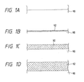
- Figs. 1A - 1D show how the pure Al or Al-Si film according to the present invention is grown.
- Fig. 1A is an illustration showing schematically the cross-section of the substrate before formation of the pure Al deposited film according to the present invention.
- 90 is the substrate comprising an electron donative material.
- the deposited film thus formed has a resistivity of, for example, with a film thickness of 400 ⁇ , 2.7 - 3.0 ⁇ ohm ⁇ cm at room temperature which is substantially equal to the bulk resistivity of Al, and becomes continuous and flat film. Also, even with a film thickness of 1 ⁇ m, its resistance at room temperature is approximately 2.7 - 3.0 ⁇ ohm ⁇ cm and a sufficiently dense film is formed with a relatively thicker film. The reflectance in the visible wavelength region is approximately 80 %, and a thin film with excellent surface flatness can be deposited.
- Fig. 2 is a schematic view showing a preferable deposition film forming device for applying the present invention.
- 1 is a substrate for forming an Al-Si film.
- the substrate 1 is mounted on a substrate holder 3 provided internally of the reaction tube 2 for forming a space for formation of a deposited film which is substantially closed to Fig. 2.
- quartz is preferable, but it may be also made of a metal. In this case, it is preferable to cool the reaction tube.
- the substrate holder 3 is made of a metal, and is provided with a heater 4 so that the substrate mounted thereon can be heated. And, the constitution is made so that the substrate temperature can be controlled by controlling the heat generation temperature of the heater 4.
- the feeding system of gases is constituted as described below.
- 5 is a gas mixer, in which the first starting gas, the second starting gas and the reaction gas are mixed, and the mixture is fed into the reaciton tube 2.
- 6 is a starting gas gasifier provided for gasification of an organic metal as the first starting gas.
- the organic metal to be used in the present invention is liquid at room temperature, and is formed into saturated vapor by passing a carrier gas through the liquid of the organic metal within the gasifier 6, which is in turn introduced into the mixer 5.
- the evacuation is constituted as described below.
- a gate valve which is opened when performing evacuation of a large volume such as during evacuation internally of the reaction tube 2 before formation of the deposited film.
- 8 is a slow leak valve, which is used when performing evacuation of a small volume such as in controlling the pressure internally of the reaction tube 2 during formation of the deposited film.
- 9 is an evacuation unit, which is constituted of a pump for evacuation such as turbo molecular pump, etc.
- the conveying system of the substrate 1 is constituted as described below.
- 10 is a substrate conveying chamber which can house the substrate before and after formation of the deposited film, which is evacuated by opening the valve 11.
- 12 is an evacuation unit for evacuating the conveying chamber, which is constituted of a pump for evacuation such as turbo molecular pump, etc.
- the valve 13 is opened only when the substrate 1 is transferred between the reaction chamber and the conveying space.
- the liquid DMAH maintained at room temperature is bubbled with H2 or Ar (or other inert gas) as the carrier gas to form gaseous DMAH, which is transported to the mixer 5.
- H2 gas as the reaction gas is transported through another route into the mixer 5.
- the gases are controlled in flow rates so that the respective partial pressures may become desired values.
- the first starting gas may be of course MMAH2, but DMAH with a vapor pressure enough to become 1 Torr at room temperature is the most preferred. Also, DMAH and MMAH2 may be used in a mixture.
- the second starting gas containing Si there can be used Si2H6, SiH4, Si3H8, Si(CH3)4, SiCl4, SiH2Cl2 and SiH3Cl.
- Si2H6 which can be easily decomposed at the low temperature of 200 - 300°C.
- the gases such as Si2H6 are diluted with H2 or Ar and transported to the mixer 5 through a system other than the DMAH system.
- the deposited film formed at a substrate temperature of 160 o C to 450 o C by use of such starting gas and reaction gas, with a thickness of for example 400 ⁇ has a resistivity at room temperature of 2.7 - 3.0 ⁇ ohm ⁇ cm which is substantially equal to Al bulk resistivity, and is a continuous and flat film.
- the pressure during film formation can be chosen within the range from 10 ⁇ 3 Torr to 760 Torr.
- the film thickness may be 1 ⁇ m
- its resistivity is ca. 2.7 - 3.0 ⁇ ohm ⁇ cm, and a sufficiently dense film can be formed also with a relatively thicker film.
- the reflectance in the visible light wavelength region is approximately 80 %, whereby a thin film excellent in surface flatness can be deposited.
- the substrate temperature is desirably the decomposition temperature of the starting gas containing Al or higher, and 450 o C or lower as described above, but specifically the substrate temperature of 200 to 450 o C is more desirable, and when deposition is carried out under this condition, by making the DMAH partial pressure 10 ⁇ 4 to 10 ⁇ 3 Torr, the deposition speed becomes very great as 100 ⁇ /min. to 800 ⁇ /min., whereby sufficient great deposition speed corresponding to the cost as the Al-Si deposition technique for ultra-LSI can be obtained.
- a more preferable substrate temperature condition is 270 o C to 350 o C, and the Al-Si film deposited under this condition is also strongly orientatable and, even when subjected to the heat treatment at 450 o C for 1 hour, the Al-Si film on the Si monocrystalline or Si polycrystalline substrate becomes a good Al-Si film without generation of hillock, spike as seen in the film forming method of the prior art. Also, such Al-Si film is excellent in electro-migration resistance.
- Al-Si can be deposited on only one sheet of substrate in deposition for one time. Although a deposition speed of ca. 800 ⁇ /min. can be obtained, it is still insufficient for performing deposition of a large number of sheets within a short time.
- the deposition film forming device for improving this point, there is the low pressure CVD device which can deposit Al-Si by simultaneous mounting of a large number of sheets of wafer. Since the Al-Si film formation according to the present invention utilizes the surface reaction on the electron donative substrate surface, in the hot wall type low pressure CVD method wherein only the substrate is heated, Al-Si compound containing 0.5 - 2.0 % of Si can be deposited on the substrate by use of DMAH and H2 and the Si starting gas such as Si2H6, etc.
- the reaction tube pressure may be 0.05 to 760 Torr, desirably 0.1 to 0.8 torr, the substrate temperature 160 o C to 450 o C, desirably 200 o C to 400 o C, the DMAH partial pressure 1 x 10 ⁇ 5-fold to 1.3 x 10 ⁇ 3-fold of the pressure in the reaction tube, the Si2H6 partial pressure 1 x 10 ⁇ 7-fold to 1 x 10 ⁇ 4-fold of the pressure in the reaction tube, and under such conditions, Al-Si can be well deposited on the electron donative substrate.
- Fig. 3 is a schematic illustration showing a deposited film forming device to which such present invention is applicable.
- 57 is a substrate for formation of Al-Si film.
- 50 is an outside reaction tube made of quartz for forming a space for formation of deposited film substantially closed to the surrounding, 51 an innerside reaction tube made of quartz located for separating the flow of gas within the outside reaction tube 50, 54 a flange made of a metal for opening and closing of the opening of the outside reaction tube 50, and the substrate 57 is located within the substrate holding member 56 provided internally of the innerside reaction tube 51.
- the substrate holding member 56 should be preferably made of quartz.
- the substrate temperature can be controlled by the heater portion 59.
- the pressure internally of the reaction tube 50 is constituted so as to be controllable by the evacuation system connected through the gas evacuation outlet 53.
- the gas feeding system is constituted to have a first gas system, a second gas system, a third gas system and a mixer (none are shown in Fig. 3) similarly as the device shown by the symbols 5 and 6 in Fig. 2, and the starting gases and the reaction gas are introduced into the reaction tube 50 through the starting gas inlet 52. These gases react on the surface of the substrate 57 during passage internally of the innerside reaction tube 51 as shown by the arrowhead 58 in Fig. 3 to deposit Al-Si on the substrate surface. The gases after the reaction pass through the gap formed between the innerside reaction tube 51 and the outside reaction tube 50, and evacuated through the gas evacuation outlet 53.
- the flange 54 made of a metal is permitted to fall by an elevator (not shown) together with the substrate holding member 56 and the substrate 57 to be moved to a predetermined position where the substrate is mounted and detached.
- Al-Si films of good quality can be formed in all the wafers within the device.
- the substrate temperature higher and DMAH partial pressure higher.
- a deposition rate of 0.2 to 0.5 ⁇ m/min. can be realized.
- the deposition rate is too large, the probability becomes higher that a surface interior in surface flatness will be obtained.
- the probability becomes higher that a pure Al or Al-Si film with a reflectance of about 10 to 30 % will be obtained.
- a film inferior in surface flatness may be considered to be due to the fact that surface migration of metal atoms or molecules are great at a high temperature, whereby deposition proceeds only at specific nuclei to deteriorate surface flatness when becoming a film thickness.
- the greatest reasons is that, at the initial stage of deposition, a film with inferior surface flatness is formed, which exerts deleterious influences even afterwards.
- the method of varying the substrate temperature and the starting gas partial pressure is used to provide a method of obtaining pure Al or Al-Si deposited film of high quality and excellent in flatness at substantially high deposition rate.
- a deposited film of pure Al or Al-Si of good quality can be formed under good selectivity at a substrate temperature of 160 to 450 °C, more preferably 270 to 350 °C.
- the first deposition step in the present invention namely the deposited film formation step at low deposition rate, under a total pressure of 10 ⁇ 3 Torr to 760 Torr, preferably 5 x 10 ⁇ 2 Torr to 5 Torr, the substrate temperature is suitably chosen from 270 to 350 °C, preferably 270 to 300 °C, and the DMAH partial pressure from 1.3 x 10 ⁇ 5 to 1.3 x 10 ⁇ 3-fold, preferably 1.3 x 10 ⁇ 5 to 1.3 x 10 ⁇ 4 -fold of the total pressure.
- the substrate temperature is made 270 to 350 °C, preferably 300 to 350 °C, and the DMAH partial pressure 1.3 x 10 ⁇ 5 to 1.3 x 10 ⁇ 3-fold of total pressure.
- the substrate temperature may be quickly elevated by irradiation of W lamp or Xe lamp on the wafer surface. Heating by a lamp is effective for quick elevation of the substrate temperature.
- the DMAH partial pressure is suitably selected from the condition of 1.3 x 10 ⁇ 4 to 1.3 x 10 ⁇ 3-fold of the total pressure, so that a deposited film may be formed at a higher deposition rate than in the deposition rate in the first step as mentioned above.
- the partial pressure of DMAH may be increased, or with the DMAH partial pressure being constant, the substrate temperature may be elevated.
- both of the substrate temperature and the partial pressure may be elevated.
- a continuous film of 100 to 200 ⁇ within the range of a substrate temperature from 270 to 300 °C in the first deposition step under the above-mentioned pressure conditions, and then form the film at an increased deposition rate of, for example, 0.1 to 1 ⁇ m/min. by increasing the substrate temperature to 300 to 350 °C.
- the deposited film thus formed becomes a film of good quality with surface migration being inhibited.
- a continuous, flat and high quality film of 100 to 200 ⁇ is formed within a deposition time of 1 to 5 minutes under the first deposition conditions, while under the second deposition conditions, since a continuous and flat pure Al (or Al-Si) has been already formed, a flat and high quality thin film can be formed even if pure Al (or Al-Si) may be deposited at a high deposition rate of 0.1 to 1 ⁇ m/min.
- a pure Al film or Al-Si film of 1 ⁇ m thickness can be sufficiently formed by deposition for 1 to 5 minutes under the first conditions, and with the deposition time for 1 to 3 minutes under the second conditions.
- pure Al or Al-Si can be deposited only on one sheet of substrate in deposition at one time.
- the method according to the present invention is also applicable to the reduced-pressure CVD device for a number of sheets as shown in Fig. 3. Since deposition according to the present invention employs the surface reaction at the heated electron donative substrate surface, according to the hot wall type reduced-pressure CVD method in which only the substrate is heated, an Al-Si containing 0.5 to 2.0 % of Si can be deposited at high speed by addition of DMAH and H2, and an Si starting gas such as Si2H6, etc., if necessary.
- the reaction tube pressure may be 0.05 to 760 Torr, desirably 0.1 to 0.8 torr.
- the substrate temperature may be 270 to 350 °C, desirably 270 to 300 °C, and the DMAH partial pressure may be 1.3 x 10 ⁇ 5 to 1.3 x 10 ⁇ 3-fold, desirably 1.3 x 10 ⁇ 5 to 1.3 x 10 ⁇ 4 of the reaction tube pressure.
- the substrate temperature is made 270 to 350 °C, preferably 300 to 350 °C, and the DMAH partial pressure 1.3 x 10 ⁇ 5 to 1.3 x 10 ⁇ 3, preferably 1.3 x 10 ⁇ 4 to 1.3 x 10 ⁇ 3-fold of the partial pressure reaction tube.
- the Si2H6 partial pressure, in both the first and the second deposition conditions, may be within the range of 1 x 10 ⁇ 7 to 1 x 10 ⁇ 4-fold of the reaction tube pressure, whereby Al-Si is deposited at high speed on the electron donative surface.
- Al-Si films of good quality can be formed in all the wafers within the device.
- a continuous and dense pure Al or Al-Si is formed, and therefore even pure Al or Al-Si may be deposited thereafter at high speed deposition conditions of 0.2 to 1 ⁇ m/min., film quality such as surface flatness, etc. will not be deteriorated, but pure Al or Al-Si film of high quality can be deposited at a high speed practically effectively.
- the film obtained is dense with little amount of impurity such as carbon, etc. contained, its resistance is similar to that of bulk, and also surface flatness is extremely high.
- the deposited film in spite of deposition at high speed, has the specific features as mentioned below:
- the through-put in the ultra-LSI process is dramatically improved.
- Al-Si can be deposited at the same time on 100 to 200 sheets of 4 inch wafer and the effect of high speed deposition contributes greatly to the improvement of through-put.
- the wafer to be used will be made to have a size of 6 or 8 inch.
- the low pressure CVD device as shown in Fig. 3 can be practically applied with difficulty, because the reaction tube diameter becomes larger.
- Al-deposition according to the CVD method of the prior art no high speed deposition of 0.2 to 1 ⁇ m/min. cannot be realized, and therefore it could be employed with difficulty even if a deposited film of high quality was formed.
- Al-Si of high quality can be deposited at high speed of 0.2 to 1 ⁇ m/min., and particularly the meaning fulfilled by the present invention in a sheet type CVD device corresponding to 6 inch or 8 inch demanded for high throughput is very important.
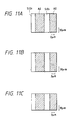
- Figs. 4A - 4E show how the Al or Al-Si film according to the present invention is selectively grown in the via-hole.
- Fig. 4A is an illustration showing schematically the cross-section of the substrate before formation of the deposited film according to the present invention.
- 90 is the substrate comprising an electron donative material, and 91 a thin film comprising an electron non-donative material.
- the film grows to the level of the uppermost portion of the thin film 91 as shown in Fig. 4D. Further, when grown under the same conditions as shown in Fig. 4E, the Al-Si film can grow to 5000 ⁇ substantially without growth in the lateral direction. This is the most characteristic point of the deposited film obtained by the present invention, and it will be understood how a film of good quality can be formed under good selectivity.
- the deposited film thus formed has a resistivity of, for example, with a film thickness of 400 ⁇ , 2.7 - 3.0 ⁇ ohm ⁇ cm at room temperature which is substantially equal to the bulk resistivity of Al, and becomes continuous and flat film. Also, even with a film thickness of 1 ⁇ m, its resistance at room temperature is approximately 2.7 - 3.0 ⁇ ohm ⁇ cm and a sufficiently dense film is formed with a relatively thicker film. The reflectance in the visible wavelength region is approximately 80 %, and a thin film with excellent surface flatness can be deposited.
- the deposition rate is shifted from a low deposition rate to a high deposition rate during the deposited film formation.
- the substrate temperature higher and DMAH partial pressure higher.
- a deposition rate of 0.2 to 0.5 ⁇ m/min. can be realized.
- the deposition rate is too large, the probability becomes higher that a surface inferior in surface flatness will be obtained.
- the probability becomes higher that a pure Al or Al-Si film with a reflectance of about 10 to 30 % will be obtained.
- a film inferior in surface flatness may be considered to be due to the fact that surface migration of metal atoms or molecules are great at a high temperature, whereby deposition proceeds only at specific nuclei to deteriorate surface flatness when becoming a film thickness.
- the greatest reasons is that, at the initial stage of deposition, a film with inferior surface flatness is formed, which exerts deleterious influences even afterwards.
- the method of varying the substrate temperature and the starting gas partial pressure is used to provide a method of obtaining pure Al or Al-Si deposited film of high quality and excellent in flatness at substantially high deposition rate.
- a deposited film of pure Al or Al-Si of good quality can be formed under good selectivity at a substrate temperature of 160 to 450 °C, more preferably 270 to 350 °C.
- the substrate temperature is suitably chosen from 270 to 350 °C, preferably 270 to 300 °C, and the DMAH partial pressure from 1.3 x 10 ⁇ 5 to 1.3 x 10 ⁇ 3-fold, preferably 1.3 x 10 ⁇ 5 to 1.3 x 10 ⁇ 4-fold of the total pressure.
- the substrate temperature is made 270 to 350 °C, preferably 300 to 350 °C, and the DMAH partial pressure 1.3 x 10 ⁇ 5 to 1.3 x 10 ⁇ 3-fold of total pressure.
- the substrate temperature may be quickly elevated by irradiation of W lamp or Xe lamp on the wafer surface. Heating by a lamp is effective for quick elevation of the substrate temperature.
- the DMAH partial pressure is suitably selected from the condition of 1.3 x 10 ⁇ 4 to 1.3 x 10 ⁇ 3-fold of the total pressure, so that a deposited film may be formed at a higher deposition rate than in the deposition rate in the first step as mentioned above.
- the partial pressure of DMAH may be increased, or with the DMAH partial pressure being constant, the substrate temperature may be elevated.
- both of the substrate temperature and the partial pressure may be elevated.
- a continuous film of 100 to 200 ⁇ within the range of a substrate temperature from 270 to 300 °C in the first deposition step under the above-mentioned pressure conditions, and then form the film at an increased deposition rate of, for example, 0.1 to 1 ⁇ m/min.by increasing the substrate temperature to 300 to 350 °C.
- the deposited film thus formed becomes a film of good quality with surface migration being inhibited.
- a continuous, flat and high quality film of 100 to 200 ⁇ is formed within a deposition time of 1 to 5 minutes under the first deposition conditions, while under the second deposition conditions, since a continuous and flat pure Al (or Al-Si) has been already formed, a flat and high quality thin film can be formed even if pure Al (or Al-Si) may be deposited at a high deposition rate of 0.1 to 1 ⁇ m/min.
- a Al film of 1 ⁇ m thickness can be sufficiently formed by deposition for 1 to 5 minutes under the first conditions, and with the deposition time for 1 to 3 minutes under the second conditions.
- Al-Si can be deposited only on one sheet of substrate in deposition at one time.
- the method according to the present invention is also applicable to the reduced-pressure CVD device for a number of sheets as shown in Fig. 3. Since Al-Si deposition according to the present invention employs the surface reaction at the heated electron donative substrate surface, according to the hot wall type reduced-pressure CVD method in which only the substrate is heated, an Al-Si containing 0.5 to 2.0 % of Si can be deposited at high speed by addition of DMAH and H2, and an Si starting gas such as Si2H6, etc., if necessary.
- the reaction tube pressure may be 0.05 to 760 Torr, desirably 0.1 to 0.8 Torr.
- the substrate temperature may be 270 to 350 °C, desirably 270 to 300 °C, and the DMAH partial pressure may be 1.3 x 10 ⁇ 5 to 1.3 x 10 ⁇ 3-fold, desirably 1.3 x 10 ⁇ 5 to 1.3 x 10 ⁇ 4 of the reaction tube pressure.
- the substrate temperature is made 270 to 350 °C, preferably 300 to 350 °C, and the DMAH partial pressure 1.3 x 10 ⁇ 5 to 1.3 x 10 ⁇ 3, preferably 1.3 x 10 ⁇ 4 to 1.3 x 10 ⁇ 3-fold of the partial pressure reaction tube.
- the Si2H6 partial pressure, in both the first and the second deposition conditions, may be within the range of 1 x 10 ⁇ 7 to 1 x 10 ⁇ 4-fold of the reaction tube pressure, whereby Al-Si is deposited at high speed on the electron donative surface.
- a continuous and dense Al-Si is formed, and therefore even Al-Si may be deposited thereafter at high speed deposition conditions of 0.2 to 1 ⁇ m/min., film quality such as surface flatness, etc. will not be deteriorated, but Al-Si film of high quality can be deposited at a high speed practically effectively.
- the through put in the ultra-LSI process is dramatically improved.
- Al-Si can be deposited at the same time on 100 to 200 sheets of 4 inch wafer, and the effect of high speed deposition contributes greatly to the improvement of through-put.
- the wafer to be used will be made to have a size of 6 or 8 inch.
- the low pressure CVD device as shown in Fig. 3 can be practically applied with difficulty, because the reaction tube diameter becomes larger.
- Al-deposition according to the CVD method of the prior art no high speed deposition of 0.2 to 1 ⁇ m/min ⁇ cannot be realized, and therefore it could be employed with difficulty even if a deposited film of high quality was formed.
- Al-Si of high quality can be deposited at high speed of 0.2 to 1 ⁇ m/min., and particularly the meaning fulfilled by the present invention in a sheet type CVD device corresponding to 6 inch or 8 inch demanded for high through-put is very important.
- the procedure for Al film formation is as follows.
- the reaction tube 2 is internally evacuated to ca. 1 x 10 ⁇ 8 Torr by the evacuation unit 9.
- Al film can be also formed if the vacuum degree within the reaction tube 2 may be higher than 1 x 10 ⁇ 8 Torr.
- the conveying chamber 10 After washing of Si wafer, the conveying chamber 10 is released to atmospheric pressure and Si wafer is mounted in the conveying chamber.
- the conveying chamber is evacuated to ca. 1 x 10 ⁇ 6 Torr, and then the gate valve 13 is opened and the wafer is mounted on the wafer holder 3.
- the gate valve 13 is closed, and the reaction chamber 2 is evacuated to a vacuum degree of ca. 1 x 10 ⁇ 8 Torr.
- DMAH is fed through the first gas line.
- the second gas line is used for H2.
- the pressure within the reaction tube 2 is made a predetermined value by controlling the opening of the slow leak valve 8.
- a typical pressure in this Example is approximately 1.5 Torr.
- the wafer is heated by current passage through the heater 4.
- DMAH is introduced into the reaction tube through the DMAH line.
- the total pressure is ca. 1.5 Torr, and the DMAH partial pressure is made ca. 1.5 x 10 5 Torr.
- Al is deposited.
- the outline of the first deposition step is as described above.
- the first deposition step after the formation of the continuous Al film of about 100 to 200 ⁇ , high speed deposition is effected at the second deposition step.
- the condition for the second deposition step are made the total pressure of ca. 1.5 Torr and the DMAH partial pressure of ca. 1 x 10 ⁇ 3 Torr.
- feeding of DMAH is stopped.
- heating of the heater 4 is stopped to cool the wafer.
- Feeding of H2 gas is stopped, and after evacuation internally of the reaction tube, the wafer is transferred to the conveying chamber, and only the conveying chamber is made atmospheric before taking out the wafer.
- the outline of Al film formation is as described above.
- Al was deposited on the Si wafer within the temperature range from 160 °C - 450°C.
- the substrate temperatures in the first and second deposition steps exceed 300 °C, high speed deposition at 0.5 to 1.0 ⁇ m was possible, but the samples that surface reflectance becomes more or less worse as compared with the case of the temperature of 300 °C or lower were found.
- the reason may be considered to be due to the fact that, if the temperature in the first deposition step is high, the possibility that flatness of the extremely thin Al film deposited in the first deposition step is slightly inferior is enhanced.
- the substrate temperature in the first deposition step is 270 °C or 300 °C, there is no difference in the results obtained.
- Example 2 when the substrate temperature in the second step exceeds 300 °C, high speed deposition at 0.5 to 1.0 ⁇ m/min. was possible.
- the difference from Example 1 is that an Al film with high surface flatness having a reflectance of 80 to 95 % could be formed even when the substrate temperature in the second step was 330 °C, 350 °C by suppressing the substrate temperature in the first deposition step at 300 °C or lower.
- This Example carries out Al deposition by use of Ar in place of H2 as the carrier gas for DMAH in the same procedure as in Example 1. From the gas second line, H2 is fed. As the result of evaluation of Al film obtained by this Example, Al was deposited on Si wafer at a temperature range of 160 °C to 450 °C similarly as in Table 1 in Example 1.
- the substrate temperatures in the first and second deposition steps exceed 300 °C, high speed deposition at 0.5 to 1.0 ⁇ m was possible, but the probability that surface reflectance becomes more or less worse is slightly enhanced. The reason may be considered to be due to the fact that, if the temperature in the first deposition step is high, flatness of the extremely thin Al film deposited in the first deposition step is inferior.
- Example 3 performs Al deposition by use of Ar in place of H2 as the carrier gas for DMAH in the same procedure as in Example 2.
- the second gas line fed H2.
- the substrate temperatures in the first deposition step were 270 °C and 300 °C, there was no difference in the results obtained.
- the film quality obtained is substantially the same as in Table 2.
- Example 1 or 2 when the substrate temperature in the second step exceeds 300 °C, high speed deposition at 0.5 to 1.0 ⁇ m/min. was possible.
- the difference from Examples 1 and 3 is that an Al film with high surface flatness having a reflectance of 80 to 95 % could be formed even when the substrate temperature in the second step was 330 °C, 350 °C by suppressing the substrate temperature in the first deposition step at 300 °C or lower.
- the Al film was formed on the substrate having the following constitution by using low pressure CVD device as shown in Fig. 3. That is, as the substrate, the following 17 kind thin films were used on the Si wafer.
- the deposition conditions at this time are as follows: during the first deposition step, Total pressure: 0.3 Torr DMAH partial pressure: 3 x 10 ⁇ 6 Torr Substrate temperature: 270°C during the second deposition step, Total pressure: 0.3 Torr DMAH partial pressure: 1 x 10 ⁇ 4 Torr Substrate temperature: 330°C
- the film quality of the Al film formed under such conditions is not different from those at a substrate temperature in the second deposition of 330°C in Table 2 as described above, and also the deposition rate in the second deposition step was very high as ca. 0.7 ⁇ m/min. for all of the substrates.
- Example 2 Al film was deposited by the use of MMAH2 in place of DAMH as the starting gas.
- the same Si wafer as in Example 1 was used.
- the deposition conditions at this time are as follows: during the first deposition step, Reaction tube pressure: 1.5 Torr MMAH2 partial pressure: 5 x 10 ⁇ 5 Torr Substrate temperature: 270°C during the second deposition step, Reaction tube pressure: 1.5 Torr MMAH2 partial pressure: 1 x 10 ⁇ 3 Torr
- the film quality of deposited Al was not different from one at a substrate temperature in the second deposition step of 330°C in Table 2.
- the deposition rate of Al in the second deposition step was ca. 0.7 ⁇ m/min. and not substantially different from the case of using DMAH.
- the procedure for Al-Si film formation is as follows.
- the reaction tube 2 is internally evacuated to ca. 1 x 10 ⁇ 8 Torr by the evacuation unit 9.
- Al-Si film can be also formed if the vacuum degree within the reaction tube 2 may be higher than 1 x 10 ⁇ 8 Torr.
- the conveying chamber 10 After washing of Si wafer, the conveying chamber 10 is released to atmospheric pressure and Si wafer is mounted in the conveying chamber.
- the conveying chamber is evacuated to ca. 1 x 10 ⁇ 6 Torr, and then the gate valve 13 is opened and the wafer is mounted on the wafer holder 3.
- the gate valve 13 is closed, and the reaction chamber 2 is evacuated to a vacuum degree of ca. 1 x 10 ⁇ 8 Torr.
- DMAH is fed through the first gas line.
- Ar is employed as the carrier gas of DMAH line.
- the second gas line is used for H2 and the third gas line for Si2H6.
- the pressure within the reaction tube 2 is made a predetermined value by controlling the opening of the slow leak valve 8.
- a typical pressure in this Example is made approximately 1.5 Torr.
- the wafer is heated by current passage through the heater 4.
- DMAH introduced into the reaction tube through the DMAH line.
- the total pressure is ca. 1.5 Torr
- the DMAH partial pressure is made ca. 1.5 x 10 ⁇ 5 Torr.
- the Si2H6 partial pressure is made 2 x 10 ⁇ 7 Torr.
- the outline of the first deposition step is as described above.
- the first deposition step after the formation of the continuous Al-Si film of about 100 to 200 ⁇ , high speed deposition is effected at the second deposition step.
- the condition for the second deposition step are made the total pressure of ca. 1.5 Torr and the DMAH partial pressure of ca. 1 x 10 ⁇ 3 Torr.
- feeding of DMAH and Si2H6 is stopped.
- heating of the heater 4 is stopped to cool the wafer.
- Feeding of H2 gas is stopped, and after evacuation internally of the reaction tube, the wafer is transferred to the conveying chamber, and only the conveying chamber is made atmospheric before taking out the wafer.
- the outline of Al film formation is as described above.
- the Al-Si films deposited by varying the substrate temperature at 13 levels were evaluated by use of various evaluation methods. The results are the same as those in Table 1.
- Al-Si was deposited on the Si wafer within the temperature range from 160°C - 450°C.
- the substrate temperatures in the first and second deposition steps exceed 300 °C, high speed deposition at 0.5 to 1.0 ⁇ m was possible, but the probability that surface reflectance becomes more or less worse is slightly enhanced. The reason may be considered to be due to the fact that, if the temperature in the first deposition step is high, flatness of the extremely thin Al-Si film deposited in the first deposition step is inferior.
- the substrate temperature in the first deposition step is 270 °C or 300 °C, there is no difference in the results obtained.
- Example 7 when the substrate temperature in the second step exceeds 300 °C, high speed deposition at 0.5 to 1.0 ⁇ m/min. was possible.
- the different from Example 7 is that an Al-Si film with high surface flatness having a reflectance of 80 to 95 % could be formed even when the substrate temperatures in the second step was were 330 °C, 350 °C.
- This Example 10 carries our Al-Si deposition by use of Ar in place or H2 as the carrier gas for DMAH in the same procedure as in Example 7. From the gas second line, H2 as the reaction gas is fed. As the result of evaluation of Al-Si film obtained by this Example, Al-Si was deposited on Si wafer at a temperature range of 160 °C to 450 °C similarly as in Table 1 in Example 1.
- the substrate temperatures in the first and second deposition steps exceed 300 °C, high speed deposition at 0.5 to 1.0 ⁇ m was possible, but the probability that surface reflectance becomes more or less worse is slightly enhanced. The reason may be considered to be due to the fact that, if the temperature in the first deposition step is high, flatness of the extremely thin Al-Si film deposited in the first deposition step is inferior.
- Example 11 performs Al-Si deposition by use of Ar in place of H2 as the carrier gas for DMAH in the same procedure as in Example 8.
- the second gas line fed H2.
- the substrate temperatures in the first deposition step were 270 °C and 300 °C, there was no difference in the results obtained.
- the film quality obtained is substantially the same as in Table 2.
- Example 7 when the substrate temperature in the second step exceeds 300 °C, high speed deposition at 0.5 to 1.0 ⁇ m/min. was possible.
- the difference from Examples 7 and 8 is that an Al-Si film with high surface flatness having a reflectance of 80 to 95 % could be formed even when the substrate temperatures in the second step were 330 °C, 350 °C
- Example 12 performs Al-Si deposition by use of Ar in place of H2 as the carrier gas for DMAH in the same procedure as in Example 9.
- Deposition condition was shown below. during the first deposition step, Total pressure: 1.5 Torr DMAH partial pressure: 1.0 x 10 ⁇ 5 Torr Substrate temperature: 270 °C during the second deposition step, Total pressure: 1.5 Torr DMAH partial pressure: 1.0 x 10 ⁇ 3 Torr Substrate temperature: 330 °C and the Si2H6 partial pressure was varied from 3 x 10 ⁇ 4 to 0.2 fold of DMAH partial pressure to effect deposition. The Si content (wt.%) of the Al-Si films were varied from 0.005 % to 5 % approximately in proportion to the Si2H6 partial pressure. As to resistivity, carbon content, average wiring life, deposition speed, hillock density and spike generation, the same results as in Example 1 were obtained.
- the Al film was formed on the substrate having the following constitution by using low pressure CVD device in Fig. 3. That is, as the substrate, (1) polycrystalline silicon (polycrystalline Si), (2) amorphous silicon (amorphous Si), (3) tungsten (W), (4) molybdenum (Mo), (5) tantalum (Ta), (6) tungsten silicide (WSi), (7) titanium silicide (TiSi), (8) aluminum (Al), (9) aluminum silicon (Al-Si), (10) titanium aluminum (Al-Ti), (11) titanium nitride (TiN), (12) copper (Cu), (13) aluminum silicon copper (Al-Si-Cu), (14) aluminum palladium (Al-Pd), (15) titanium (Ti), (16) molybdenum silicide (Mo-Si), (17) tantalum silicide (Ta-Si) were employed.
- the deposition conditions at this time are as follows: during the first deposition step, Total pressure: 0.3 Torr DMAH partial pressure: 3 x 10 ⁇ 6 Torr Si2H6 partial pressure: 1.0 x 10 ⁇ 7 Torr Substrate temperature: 270°C during the second deposition step, Total pressure: 0.3 Torr DMAH partial pressure: 1 x 10 ⁇ 4 Torr Si2H6 partial pressure: 3 x 10 ⁇ 6 Torr Substrate temperature: 330°C
- the film quality of the Al-Si film formed under such conditions is not different from those at a substrate temperature in the second deposition of 330°C in Table 2 as described above, and also the deposition rate in the second deposition step was very high as ca. 0.7 ⁇ m/min. for all of the substrates.
- the deposition conditions at this time are as follows: during the first deposition step, Reaction tube pressure: 1.5 Torr MMAH2 partial pressure: 5 x 10 ⁇ 5 Torr Si2H6 partial pressure: 1.0 x 10 ⁇ 6 Torr Substrate temperature: 270°C during the second deposition step, Reaction tube pressure: 1.5 Torr MMAH2 partial pressure: 1 x 10 ⁇ 3 Torr Si2H6 partial pressure: 1 x 10 ⁇ 5 Torr
- the film quality of deposited Al-Si was not different from one at a substrate temperature in the second deposition step of 330°C in Table 2.
- the deposition rate of Al-Si in the second deposition step was ca. 0.7 ⁇ m/min. and not substantially different from the case of using DMAH.
- Al-Si film was deposited by the use of SiH4 in place of Si2H6.
- Si wafer was used as the substrate.
- the deposition conditions at this time are as follows: during the first deposition step, Reaction tube pressure: 1.5 Torr DMAH partial pressure: 1.0 x 10 ⁇ 5 Torr Si2H6 partial pressure: 5.0 x 10 ⁇ 7 Torr Substrate temperature: 270°C during the second deposition step, Reaction tube pressure: 1.5 Torr DMAH partial pressure: 1 x 10 ⁇ 3 Torr Si2H6 partial pressure: 5 x 10 ⁇ 5 Torr Substrate temperature: 330°C
- the film quality of deposited Al-Si was not different from one at a substrate temperature in the second deposition step of 330°C in Table 2.
- the deposition rate of Al-Si in the second deposition step was ca. 0.7 ⁇ m/min. and not substantially different from the case of using Si2H6.
- the crystal direction of the Si substrate is (111) plane
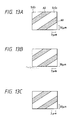
- Fig. 5 When the crystal direction of the Si substrate is (111) plane, from X-ray diffraction, as shown in Fig. 5, only the diffraction peak showing Al (100) was observed concerning Al.
- Fig. 6A is a diffraction pattern when electron beam is permitted to enter Al (100) in the [001] direction
- Fig. 6B a diffraction pattern when electron beam is permitted to enter Al (100) in the direction of [011].
- the Al film of the Si (111) substrate was found to be a monocrystal having (100) plane.
- those deposited at a range from 250 o C to 330 o C were found to have Al films reproducibly deposited which were monocrystalline.
- the Al films deposited on the Si (111) substrate with the substrate surface having off-angles differing by 1 o , 2 o , 3 o , 4 o , 5 o from the Si (111) plane were also found to have Al (100) monocrystals deposited stably, particularly under the temperature conditions of the first and second substrate temperature ranging from 250 o C to 330 o C, similarly as in the case when deposited on the Si (111) substrate as described above.
- the Al films deposited on the Si (100) substrate with the substrate surface having off-angles differing by 1 o , 2 o , 3 o , 4 o , 5 o from the Si (100) plane were also found to have Al (111) monocrystals deposited stably, particularly under the temperature conditions of the first and second substrate temperature ranging from 250 o C to 330 o C, similarly as in the case when deposited on the Si (111) substrate as described above.
- Fig. 6A is a diffraction pattern when electron beam is permitted to enter Al (100) in the [001] direction
- Fig. 6B a diffraction pattern when electron beam is permitted to enter Al (100) in the direction of [011].
- the Al film on the Si (111) substrate was found to be a monocrystal having (100) plane.
- those deposited at a range from 250 o C to 330 o C were found to have Al films deposited which were monocrystalline.
- the Al films deposited on the Si (111) substrate with the substrate surface having off-angles differing by 1 o , o , 3 o , 4 o , 5 o from the Si (111) plane were also found to have Al (100) monocrystals deposited stably, particularly under the temperature conditions of the second substrate temperature ranging from 250 o C to 330 o C, similarly as in the case when deposited on the Si (111) substrate as described above.
- the crystals direction of the Si substrate is (100) plane, from X-ray diffraction, as shown in Fig. 7, only the diffraction peak showing Al (111) was observed concerning Al.
- a monocrystal spot showing Al (11) was observed.
- the Al film on the Si (100) substrate was found to be a monocrystal having (111) plane.
- those deposited at a range from 250 o C to 330 o C were found to have Al films deposited which were stably monocrystalline.
- the Al films deposited on the Si (100) substrate with the substrate surface having off-angles differing by 1 o , 2 o , 3 o , 4 o , 5 o from the Si (100) plane were also found to have Al (111) monocrystals deposited stably, particularly under the temperature conditions of the second substrate temperature ranging from 250 o C to 330 o C, similarly as in the case when deposited on the Si (111) substrate as described above.
- Example 3 Crystallinity of the Al film formed by the method of Example 3 was examined. Similarly as in the case of Example 1, at a substrate temperature of the first and second substrate in Table 2 ranging from 250°C to 330°C, Al(100) monocrystal was deposited on the Si (111) substrate, and Al (111) monocrystal on the Si (100) substrate.
- Example 4 Crystallinity of the Al film formed by the method of Example 4 was examined. Similarly as in the case of Example 1, at a substrate temperature of the first and second substrate in Table 2 ranging from 270°C to 330°C, Al (100) monocrystal was deposited on the Si (111) substrate, and Al (111) monocrystal on the Si (100) substrate.
- the procedure for Al film formation is as follows.
- the reaction tube 2 is internally evacuated to ca. 1 x 10 ⁇ 8 Torr by the evacuation unit 9.
- Al film can be also formed if the vacuum degree within the reaction tube 2 may be higher than 1 x 10 ⁇ 8 Torr.
- the conveying chamber 10 After washing of Si wafer, the conveying chamber 10 is released to atmospheric pressure and Si wafer is mounted in the conveying chamber.
- the conveying chamber is evacuated to ca. 1 x 10 ⁇ 6 Torr, and then the gate valve 13 is opened and the wafer is mounted on the wafer holder 3.
- the gate valve 13 is closed, and the reaction chamber 2 is evacuated to a vacuum degree of ca. 1 x 10 ⁇ 8 Torr.
- DMAH is fed through the first gas line.
- the second gas line is used for H2.
- the pressure within the reaction tube 2 is made a predetermined value by controlling the opening of the slow leak valve 8.
- a typical pressure in this Example is made approximately 1.5 Torr.
- the wafer is heated by current passage through the heater 4.
- DMAH is introduced into the reaction tube through the DMAH line.
- the total pressure is ca. 1.5 Torr, and the DMAH partial pressure is made ca. 1.5 x 10 ⁇ 4 Torr.
- Al is deposited.
- the outline of the first deposition step is as described above.
- the first deposition step after the formation of the continuous Al film of about 100 to 200 ⁇ , high speed deposition is effected at the second deposition step.
- the condition for the second deposition step are made the total pressure of ca. 1.5 Torr and the DMAH partial pressure of ca. 1 x 10 ⁇ 3 Torr.
- feeding of DMAH is stopped.
- heating of the heater 4 is stopped to cool the wafer.
- Feeding of H2 gas is stopped, and after evacuation internally of the reaction tube, the wafer is transferred to the conveying chamber, and only the conveying chamber is made atmospheric pressure before taking out the wafer.
- the outline of Al film formation is as described above.
- Si substrates (N type, 1 - 2 ohm ⁇ cm) were subjected to thermal oxidation at a temperature of 1000 o C according to the hydrogen combustion system (H2: 4 liters/M, O2: 2 liters/M).
- the film thickness was 7000 ⁇ ⁇ 500 ⁇ , and the refractive index 1.46.
- a photoresist was coated on the whole Si substrate, and a desired pattern was baked by an exposure machine. The pattern was such that various holes of 0.25 ⁇ m x 0.25 ⁇ m - 100 ⁇ m x 100 ⁇ m were opened. After development of the resist, with the photoresist as the mask, the subbing SiO2 was etched by the reactive ion etching (RIE), etc. to have the substrate Si partially exposed.
- RIE reactive ion etching
- the substrate temperatures in the first and second deposition steps exceed 300 °C, high speed deposition at 0.5 to 1.0 ⁇ m was possible, but the probability that surface reflectance becomes more or less worse as compared with the case of 300°C or lower is slightly enhanced.
- the reason may be considered to be due to the fact that, if the temperature in the first deposition step is high, flatness of the extremely thin Al film deposited in the first deposition step is inferior.
- the substrate temperature in the first deposition step is 270 °C or 300 °C, there is no difference in the results obtained.
- Example 20 when the substrate temperature in the second step exceeds 300 °C, high speed deposition at 0.5 to 1.0 ⁇ m/min. was possible.
- the difference from Example 20 is that an Al film with high surface flatness having a reflectance of 80 to 95 % could be formed even when the substrate temperature in the second step was 330 °C, 350 °C.
- Example 20 Al was selectively deposited only on Si. Also, even when Al was deposited to 2 ⁇ m, the selective depositability was maintained.
- This Example 22 carries out Al deposition by use of Ar in place of H2 as the carrier gas for DMAH in the same procedure as in Example 20. From the gas second line, H2 is fed.
- the substrate temperatures in the first and second deposition steps exceed 300 °C, high speed deposition at 0.5 to 1.0 ⁇ m was possible, but the probability that surface reflectance becomes more or less worse is slightly enhanced. The reason may be considered to be due to the fact that, if the temperature in the first deposition step is high, flatness of the extremely thin Al film deposited in the first deposition step is inferior.
- This Example 23 performed Al deposition by use of Ar in place of H2 as the carrier gas for DMAH in the same procedure as in Example 21.
- the second gas line fed H2.
- the substrate temperatures in the first deposition step were 270 °C and 300 °C, there was no difference in the results obtained.
- the film quality obtained is substantially the same as in Table 4.
- Example 20 or 21 when the substrate temperature in the second step exceeds 300 °C, high speed deposition at 0.5 to 1.0 ⁇ m/min. was possible.
- the difference from Examples 20 and 21 is that an Al film with high surface flatness having a reflectance of 80 to 95 % could be reproducibly formed even when the substrate temperature in the second step was 330 °C, 350 °C.
- Example 20 Al was selectively deposited only on Si. Also, even when Al was deposited to 2 ⁇ m, the selective depositability was maintained.
- a thermally oxidized SiO2 film as the electron non-donative second substrate surface material was formed, and patterning was effected according to the photolithographic steps as shown in Example 20 to have the monocrystalline surface partially exposed.
- thermally oxidized SiO2 (hereinafter abbreviated as T-SiO2)/monocrystalline silicon").
- Samples 5-11 - 5-179 shown in Table 5 were prepared.
- the deposition conditions were as follows: during the first deposition step, Total pressure: 0.3 Torr DMAH partial pressure: 3 x 10 ⁇ 6 Torr Substrate temperature: 270°C during the second deposition step, Total pressure: 0.3 Torr DMAH partial pressure: 1 x 10 ⁇ 4 Torr Substrate temperature: 330°C
- the film quality of the Al film formed is not different from those at a substrate temperature in the second deposition of 330°C in Table 2 as described above, and also the deposition rate in the second deposition step was very high as ca. 0.7 ⁇ m/min. for all of the substrates.
- Al film was deposited by the use of MMAH2 in place of DMAH.
- Si wafer obtained by patterning the same SiO2 thin film as shown in Example 20.
- the deposition conditions at this time are as follows: during the first deposition step, Reaction tube pressure: 1.5 Torr MMAH2 partial pressure: 5 x 10 ⁇ 5 Torr Substrate temperature: 270°C during the second deposition step, Reaction tube pressure: 1.5 Torr MMAH2 partial pressure: 1 x 10 ⁇ 3 Torr
- the deposition rate of Al in the second deposition step was ca. 0.7 ⁇ m/min. and not substantially different from the case of using DMAH.
- the procedure for Al-Si film formation is as follows.
- the reaction tube 2 is internally evacuated to ca. 1 x 10 ⁇ 8 Torr by the evacuation unit 9.
- Al-Si film can be also formed if the vacuum degree within the reaction tube 2 may be higher than 1 x 10 ⁇ 8 Torr.
- the conveying chamber 10 After washing of Si wafer, the conveying chamber 10 is released to atmospheric pressure and Si wafer is mounted in the conveying chamber.
- the conveying chamber is evacuated to ca. 1 x 10 ⁇ 6 Torr, and then the gate valve 13 is opened and the wafer is mounted on the wafer holder 3.
- the gate valve 13 is closed, and the reaction chamber 2 is evacuated to a vacuum degree of ca. 1 x 10 ⁇ 8 Torr.
- DMAH is fed through the first gas line.
- the second gas line is used for H2 and the third gas line for Si2H6.
- the pressure within the reaction tube 2 is made a predetermined value by controlling the opening of the slow leak valve 8.
- a typical pressure in this Example is made approximately 1.5 Torr.
- the wafer is heated by current passage through the heater 4.
- DMAH is introduced into the reaction tube through the DMAH line.
- the total pressure is ca. 1.5 Torr
- the DMAH partial pressure is made ca. 1.5 x 10 ⁇ 5 Torr.
- the Si2H6 partial pressure is made 2 x 10 ⁇ 7 Torr.
- the outline of the first deposition step is as described above.
- the first deposition step after the formation of the continuous Al-Si film of about 100 to 200 ⁇ , high speed deposition is effected at the second deposition step.
- the condition for the second deposition step are made the total pressure of ca. 1.5 Torr, the DMAH partial pressure of ca. 1 x 10 ⁇ 3 Torr and the Si2H6 partial pressure of ca. 1.5 x 10 ⁇ 5 Torr.
- feeding of DMAH and Si2H6 is stopped.
- heating of the heater 4 is stopped to cool the wafer.
- Feeding of H2 gas is stopped, and after evacuation internally of the reaction tube, the wafer is transferred to the conveying chamber, and only the conveying chamber is made atmospheric pressure before taking out the wafer.
- the outline Al film formation is as described above.
- Si substrates (N type, 1 - 2 ohm ⁇ cm) were subjected to thermal oxidation at a temperature of 1000 o C according to the hydrogen combustion system (H2: 4 liters/M, O2: 2 liters/M).
- the film thickness was 7000 ⁇ ⁇ 500 ⁇ , and the refractive index 1.46.
- a photoresist was coated on the whole Si substrate, and a desired pattern was baked by an exposure machine. The pattern was such that various holes of 0.25 ⁇ m x 0.25 ⁇ m - 100 ⁇ m x 100 ⁇ m were opened. After development of the resist, with the photoresist as the mask, the subbing SiO2 was etched by the reactive ion etching (RIE), etc. to have the substrate Si partially exposed.
- RIE reactive ion etching
- the substrate temperatures in the first and second deposition steps exceed 300 °C, high speed deposition at 0.5 to 1.0 ⁇ m was possible, but the probability that surface reflectance becomes more or less worse is slightly enhanced. The reason may be considered to be due to the fact that, if the temperature in the first deposition step is high, flatness of the extremely thin Al-Si film deposited in the first deposition step is inferior.
- the substrate temperature in the first deposition step is 270 °C or 300 °C, there is no difference in the results obtained.
- Example 20 when the substrate temperature in the second step exceeds 300 °C, high speed deposition at 0.5 to 1.0 ⁇ m/min. was possible.
- the difference from Example 20 is that an Al-Si film with high surface flatness having a reflectance of 80 to 95 % could be formed even when the substrate temperature in the second step was 330 °C, 350 °C.
- Example 20 Al-Si was selectively deposited only on Si. Also, even when Al-Si was deposited to 2 ⁇ m, the selective depositability was maintained.
- Example 27 the selective depositability based on the substrate surface material was confirmed at the whole region.
- Example 29 performs Al-Si deposition by use of Ar in place of H2 as the carrier gas for DMAH in the same procedure as in Example 26.
- the substrate temperatures in the first and second deposition steps exceed 300 °C, high speed deposition at 0.5 to 1.0 ⁇ m/min. was possible, but the probability that surface reflectance becomes more or less worse is slightly enhanced. The reason may be considered to be due to the fact that, if the temperature in the first deposition step is high, flatness of the extremely thin Al-Si film deposited in the first deposition step is inferior.
- This Example 30 performs Al-Si deposition by use of Ar in place of H2 as the carrier gas for DMAH in the same procedure as in Example 27.
- the second gas line fed H2.
- the substrate temperatures in the first deposition step were 270 °C and 300 °C, there was no difference in the results obtained.
- the film quality obtained is substantially the same as in Table 4.
- Example 7 or 27 when the substrate temperature in the second step exceeds 300 °C, high speed deposition at 0.5 to 1.0 ⁇ m/min. was possible.
- the difference from Examples 26 and 27 is that an Al-Si film with high surface flatness having a reflectance of 80 to 95 % could be formed even when the substrate temperature in the second step were 330 °C and 350 °C.
- Example 26 and 27 Al selectively deposited only on Si. Also, even when Al-Si was deposited to 2 ⁇ m, the selective depositability was maintained.
- Example 31 performs Al-Si deposition by use of Al in place of H2 as the carrier gas for DMAH in the same procedure as in Example 28.
- Deposition condition was shown below. during the first deposition step, Total pressure: 1.5 Torr DMAH partial pressure: 1.0 x 10 ⁇ 5 Torr Substrate temperature: 270 °C during the second deposition step, Total pressure: 1.5 Torr DMAH partial pressure: 1.0 x 10 ⁇ 3 Torr Substrate temperature: 330 °C and the Si2H6 partial pressure was varied from 3 x 10 ⁇ 4 to 0.2 fold of DMAH partial pressure to effect deposition. Similarly as in Example 28, the Si content (we.%) of the Al-Si films were varied from 0.005 % to 5 % approximately in proportion to the Si2H6 partial pressure.
- Example 20 As to resistivity, carbon content, average wiring life, deposition speed, hillock density and spike generation, the same results as in Example 20 were obtained. However, in samples having an Si content of 4 % or higher, deposition was generated in the films which appeared to be Si to worsen slightly surface morphology, thereby making the reflectance 65 % or lower. Samples having a Si content of less than 4 % exhibited a reflectance of 80 to 95 %, which was similarly good the same as in Example 27.
- Example 26 the selective depositability based on the substrate surface material was confirmed at the whole region.
- a thermally oxidized SiO2 film as the electron non-donative second substrate surface material was formed, and patterning was effected according to the photolithographic steps as shown in Example 7 to have the monocrystalline surface partially exposed.
- thermally oxidized SiO2 (hereinafter abbreviated as T-SiO2)/monocrystalline silicon").
- Samples 5-11 - 5-179 shown in Table 5 were prepared.
- the deposition conditions were as follows: during the first deposition step, Total pressure: 0.3 Torr DMAH partial pressure: 3 x 10 ⁇ 6 Torr Si2H6 partial pressure: 1 x 10 ⁇ 7 Torr Substrate temperature: 270°C during the second deposition step, Total pressure: 0.3 Torr DMAH partial pressure: 1 x 10 ⁇ 4 Torr Si2H6 partial pressure: 3 x 10 ⁇ 6 Torr Substrate temperature: 330°C
- the film quality of the Al-Si film formed is not different from those at a substrate temperature in the second deposition of 330°C in Table 2 as described above, and also the deposition rate in the second deposition step was very high as ca. 0.7 ⁇ m/min. for all of the substrates.
- Example 27 Al-Si film was deposited by the use of MMAH2 in place of DMAH.
- Si wafer obtained by patterning the same SiO2 thin film as shown in Example 26.
- the deposition conditions at this time are as follows: during the first deposition step, Reaction tube pressure: 1.5 Torr MMAH2 partial pressure: 5 x 10 ⁇ 5 Torr Si2H6 partial pressure: 1 x 10 ⁇ 6 Torr Substrate temperature: 270°C during the second deposition step, Reaction tube pressure: 1.5 Torr MMAH2 partial pressure: 1 x 10 ⁇ 3 Torr Si2H6 partial pressure: 1 x 10 ⁇ 5 Torr
- Example 27 Al-Si film embedded completely the SiO2 opening with the depth of 7000 ⁇ and the film quality of deposited Al-Si was not different from one at a substrate temperature in the second deposition step of 330°C in Table 2.
- the deposition rate of Al-Si in the second deposition step was ca. 0.7 ⁇ m/min. and not substantially different from the case of using DMAH.
- the deposition conditions at this time are as follows: during the first deposition step, Reaction tube pressure: 1.5 Torr DMAH partial pressure: 1 x 10 ⁇ 5 Torr Si2H6 partial pressure: 5 x 10 ⁇ 7 Torr Substrate temperature: 270°C during the second deposition step, Reaction tube pressure: 1.5 Torr DMAH partial pressure: 1 x 10 ⁇ 3 Torr Si2H6 partial pressure: 5 x 10 ⁇ 5 Torr Substrate temperature: 330°C
- Example 27 Al-Si film embedded completely the SiO2 opening with the depth of 7000 ⁇ and the film quality of deposited Al-Si was not different from one at a substrate temperature in the second deposition step of 330°C in Table 4.
- the deposition rate of Al-Si in the second deposition step was ca. 0.7 ⁇ m/min. and not substantially different from the case of using Si2H6.
- Example 20 a sample having an Al film formed thereon was prepared.
- the crystallinity of the Al film selectively deposited on Si at the same substrate temperature as in Table 1 was evaluated by the X-ray diffraction method and the scanning ⁇ -RHEED microscope.
- the scanning ⁇ -RHEED microscope is the method disclosed in Extended Abstracts of the 21th Conference on Solid State Devices and Materials (1989) p.217 and Japanese Journal of Applied Physics vol. 28, No. 11 (1989), L2075.
- RHEED Reflect High Energy Electron Diffraction
- electron beam was permitted to be incident on the sample surface at a shallow angle of 2 - 3 o , and the crystallinity of the sample surface was evaluated from the diffraction pattern formed by the diffracted electron beam.
- the electron beam diameter is large as 100 ⁇ m to several hundred ⁇ m, only average information on the sample surface could be obtained.
- an electron beam diffraction pattern from a specific fine region on the sample surface can be observed by narrowing the electron beam diameter of 0.1 ⁇ m. Also, by scanning the electron beam two-dimensionally on the sample surface, by use of any desired diffraction spot intensity change on the diffraction pattern as the image signal, two dimensional image (scanning ⁇ -RHEED image) on the sample surface can be obtained. At this time by observation of the scanning ⁇ -RHEED image by use of different diffraction spots A and C on the diffraction pattern as shown in Fig.
- the diffraction spot A is a diffraction spot on the line (line 1) where the plane in which the diffraction pattern occurs and the sagittal plane formed by the incident electron beam are crossed at right angle, while the diffraction spot C is a diffraction spot not on the line 1.
- line 1 the line in which the diffraction pattern occurs and the sagittal plane formed by the incident electron beam are crossed at right angle
- the diffraction spot C is a diffraction spot not on the line 1.
- the Al selectively deposited was found to be similarly Al (100) monocrystal. Those at substrate temperature ranging from 250 o C to 330 o C were selectively deposited stably, and the Al obtained was found to become monocrystal.
- Al films deposited selectively on the Si (111) substrate with the Si (111) plane being at off-angles by 1 o , 2 o , 3 o , 4 o , 5 o from the Si substrate were also found to deposit Al (100) monocrystals under the temperature conditions of the substrate temperature ranging from 250 o to 330 o C similarly as deposited on the Si (111) substrate as described above.
- Fig. 13 shows the scanning secondary electron image (Fig. 13A) and the scanning ⁇ -RHEED image (Figs. 13B and 13C) when Al was selectively deposited on only the Si exposed surface on a substrate having Si (100) exposed in a line by patterning of SiO2 in a line.
- the scanning ⁇ -RHEED image the 333 diffraction spots (Fig. 13B) and 531 diffraction spots (Fig. 13C) were employed.
- the Al film selectively deposited was confirmed to be an Al (111) monocrystal. Those at substrate temperatures ranging from 250 o C to 330 o C were found to be selectively deposited stably, and the Al films obtained became monocrystals.
- Al films deposited selectively on the Si (100) substrate with the Si (100) plane being at off-angles by 1 o , 2 o , 3 o , 4 o , 5 o from the Si substrate surface were also found to deposit Al (111) monocrystals under the temperature conditions of the substrate temperature ranging from 250 o C to 330 o C similarly as deposited on the Si (111) substrate as described above.
- the Al films deposited on the Si (111) substrate with the substrate surface having off-angles differing by 1 o , 2 o , 3 o , 4 o , 5 o from the Si (111) plane were also found to have Al (100) monocrystals deposited stably under the temperature conditions of the first and second substrate temperature ranging from 250 o C to 330 o C similarly as in the case when deposited on the Si (111) substrate as described above.
- the Al films deposited on the Si (100) substrate with the substrate surface having off-angles differing by 1 o , 2 o , 3 o , 4 o , 5 o from the Si (100) plane were also found to have Al (111) monocrystals deposited under the temperature conditions of the second substrate temperature ranging from 270 o C to 330 o C, similarly as in the case when deposited on the Si (111) substrate as described above.
- Example 22 Crystallinity of the Al film selectively deposited by the method of Example 22 was examined. Similarly as in the case of Example 20, at a substrate temperature of the first and second substrate in Table 2 ranging from 250°C to 330°C, Al(100) monocrystal was deposited on the Si (111) substrate, and Al (111) monocrystal on the Si (100) substrate.
- Example 23 Crystallinity of the Al film selectively deposited by the method of Example 23 was examined. Similarly as in the case of Example 1, at a substrate temperature of the second substrate in Table 2 ranging from 270°C to 330°C, Al (100) monocrystal was deposited on the Si (111) substrate, and Al (111) monocrystal on the Si (100) substrate.
- the Al selectively deposited on Si was found to be Al (100).
- the Al film selectively deposited was found to be Al (111).
- the Al film selectively deposited was found to be oriented in Al (111) from X-ray diffraction, and from reflective high speed electron beam diffraction pattern of the prior art by use of an electron beam of an acceleration voltage of 80 kV or 100 kV, diffraction spots concerned with Al (111) were strongly observed.
- a polycrystalline silicon layer was formed by the thermal CVD method, a polycrystalline silicon gate electrode 504 was formed, and also with the thick field oxidized film and the gate electrode 504 as the mask, phosphorus was ion injected self-matchingly to form an impurity diffused region 505 of 1 x 1018 cm ⁇ 3 (Fig. 14B).
- an oxidized silicon film 508 was formed by use of the thermal CVD method (Fig. 14C).
- a contact hole 509 with a size of 0.5 ⁇ m x 0.5 ⁇ m was formed (Fig. 14D).
- the substrate temperature was made 270 °C, and DMAH was employed as the starting gas, H2 as the carrier gas to carry out formation of Al film.
- the transistor After completion of formation of Al film, the transistor was taken out from the film forming device and observed. As the result, it was found that Al film 510 was deposited only on the Si 505 wherein phosphorus was diffused in the contact hole 509, and not deposited on the oxidized film 508 (Fig. 14E). Further, the surface of the Al film 510 was very flat. When the characteristics of the transistor obtained were examined, extremely good characteristics were exhibited.
- the substrate was made N type and the impurity was changed from phosphorus to boron to prepare P channels MoS.
- An Al film was formed on a monocrystalline silicon under the following conditions.
- Resistivity became greater by 2-fold or more than the case when hydrogen was employed.
- Al deposited only by decomposition of DMAH without use of H2 is inferior in film quality, and was unsatisfactory as the Al film for a semiconductor device.
- DMAH DMAH was decomposed by the optical CVD method to deposit Al.
- some improvement such as no containment of carbon, and the like was observed from as the Al film prepared as compared with the case when no light was employed, but other characteristics were not improved so much, and the Al film was still unsatisfactory as the Al film for a semiconductor device.
- the mechanism of Al deposition according to the present invention may be presently hypothesized as follows.
- Figs. 15A - 15D are illustrations for better understanding of the reacion mechanism, and the numbers of H, e and Al shown in Figs. 15A - 15D are not necessarily coincident.
- Si atoms are incorporated into Al during the process of the reaction as described above.
- a low resistivity, dense and flat Al or Al-Si film could be deposited on a substrate at high speed.
- Average wiring life is time to wire breaking when current is passed at a current density of 1 x 10⁶ A/cm2 through a cross-sectional area of 1 ⁇ m2 at 250°C.
- Spike generation ratio is destruction probability at the junction portion of 0.15 ⁇ m depth.
Landscapes
- Engineering & Computer Science (AREA)
- General Physics & Mathematics (AREA)
- Physics & Mathematics (AREA)
- Condensed Matter Physics & Semiconductors (AREA)
- Manufacturing & Machinery (AREA)
- Computer Hardware Design (AREA)
- Microelectronics & Electronic Packaging (AREA)
- Power Engineering (AREA)
- General Chemical & Material Sciences (AREA)
- Chemical Kinetics & Catalysis (AREA)
- Chemical & Material Sciences (AREA)
- Internal Circuitry In Semiconductor Integrated Circuit Devices (AREA)
- Electrodes Of Semiconductors (AREA)
- Chemical Vapour Deposition (AREA)
Applications Claiming Priority (8)
| Application Number | Priority Date | Filing Date | Title |
|---|---|---|---|
| JP250022/89 | 1989-09-26 | ||
| JP250023/89 | 1989-09-26 | ||
| JP25002389 | 1989-09-26 | ||
| JP25002289 | 1989-09-26 | ||
| JP6560/90 | 1990-01-16 | ||
| JP2006559A JP2721020B2 (ja) | 1989-09-26 | 1990-01-16 | 堆積膜形成法 |
| JP6559/90 | 1990-01-16 | ||
| JP2006560A JP2721021B2 (ja) | 1989-09-26 | 1990-01-16 | 堆積膜形成法 |
Publications (3)
| Publication Number | Publication Date |
|---|---|
| EP0420597A2 true EP0420597A2 (de) | 1991-04-03 |
| EP0420597A3 EP0420597A3 (en) | 1991-08-21 |
| EP0420597B1 EP0420597B1 (de) | 1996-04-24 |
Family
ID=27454510
Family Applications (1)
| Application Number | Title | Priority Date | Filing Date |
|---|---|---|---|
| EP90310508A Expired - Lifetime EP0420597B1 (de) | 1989-09-26 | 1990-09-25 | Verfahren zur Herstellung einer abgeschiedenen Schicht unter Verwendung von Alkylaluminiumhydrid und Verfahren zur Herstellung eines Halbleiterbauelements |
Country Status (8)
| Country | Link |
|---|---|
| US (1) | US5316972A (de) |
| EP (1) | EP0420597B1 (de) |
| KR (1) | KR940007444B1 (de) |
| AT (1) | ATE137357T1 (de) |
| DE (1) | DE69026669T2 (de) |
| MY (1) | MY136962A (de) |
| PT (1) | PT95431B (de) |
| SG (1) | SG45420A1 (de) |
Cited By (3)
| Publication number | Priority date | Publication date | Assignee | Title |
|---|---|---|---|---|
| EP0514888A1 (de) * | 1991-05-23 | 1992-11-25 | Canon Kabushiki Kaisha | Verfahren zur Bildung einer Kontaktfläche durch selektives Niederschlagen von einem Metallfilm |
| EP0572212A2 (de) * | 1992-05-29 | 1993-12-01 | STMicroelectronics, Inc. | Herstellungsverfahren von mit Silizium datiertem Aluminium durch CVD |
| US6627547B2 (en) | 1996-08-01 | 2003-09-30 | Cypress Semiconductor Corporation | Hot metallization process |
Families Citing this family (12)
| Publication number | Priority date | Publication date | Assignee | Title |
|---|---|---|---|---|
| EP0460857B1 (de) * | 1990-05-31 | 1997-03-19 | Canon Kabushiki Kaisha | Verfahren zur Herstellung einer Halbleitervorrichtung mit einer Verdrahtungsstruktur hoher Dichte |
| EP0608628A3 (de) * | 1992-12-25 | 1995-01-18 | Kawasaki Steel Co | Verfahren zur Herstellung einer Halbleitervorrichtung mit Mehrlagen-Verbindungsstruktur. |
| US6159854A (en) * | 1994-08-22 | 2000-12-12 | Fujitsu Limited | Process of growing conductive layer from gas phase |
| US5877087A (en) | 1995-11-21 | 1999-03-02 | Applied Materials, Inc. | Low temperature integrated metallization process and apparatus |
| US6726776B1 (en) | 1995-11-21 | 2004-04-27 | Applied Materials, Inc. | Low temperature integrated metallization process and apparatus |
| US6077781A (en) * | 1995-11-21 | 2000-06-20 | Applied Materials, Inc. | Single step process for blanket-selective CVD aluminum deposition |
| US6025269A (en) * | 1996-10-15 | 2000-02-15 | Micron Technology, Inc. | Method for depositioning a substantially void-free aluminum film over a refractory metal nitride layer |
| US6156645A (en) * | 1996-10-25 | 2000-12-05 | Cypress Semiconductor Corporation | Method of forming a metal layer on a substrate, including formation of wetting layer at a high temperature |
| US6187673B1 (en) * | 1998-09-03 | 2001-02-13 | Micron Technology, Inc. | Small grain size, conformal aluminum interconnects and method for their formation |
| US6245655B1 (en) * | 1999-04-01 | 2001-06-12 | Cvc Products, Inc. | Method for planarized deposition of a material |
| US6207558B1 (en) | 1999-10-21 | 2001-03-27 | Applied Materials, Inc. | Barrier applications for aluminum planarization |
| US11261533B2 (en) * | 2017-02-10 | 2022-03-01 | Applied Materials, Inc. | Aluminum plating at low temperature with high efficiency |
Family Cites Families (20)
| Publication number | Priority date | Publication date | Assignee | Title |
|---|---|---|---|---|
| US4497683A (en) * | 1982-05-03 | 1985-02-05 | At&T Bell Laboratories | Process for producing dielectrically isolated silicon devices |
| JPS6211227A (ja) * | 1985-07-09 | 1987-01-20 | Fujitsu Ltd | 半導体装置の製造方法 |
| US4824802A (en) * | 1986-02-28 | 1989-04-25 | General Electric Company | Method of filling interlevel dielectric via or contact holes in multilevel VLSI metallization structures |
| JPS62216224A (ja) * | 1986-03-17 | 1987-09-22 | Fujitsu Ltd | タングステンの選択成長方法 |
| JP2559030B2 (ja) * | 1986-07-25 | 1996-11-27 | 日本電信電話株式会社 | 金属薄膜の製造方法 |
| JP2534848B2 (ja) * | 1986-09-08 | 1996-09-18 | 富士通株式会社 | 高融点金属の選択成長法 |
| US4960732A (en) * | 1987-02-19 | 1990-10-02 | Advanced Micro Devices, Inc. | Contact plug and interconnect employing a barrier lining and a backfilled conductor material |
| EP0305143B1 (de) * | 1987-08-24 | 1993-12-08 | Fujitsu Limited | Verfahren zur selektiven Ausbildung einer Leiterschicht |
| US4786615A (en) * | 1987-08-31 | 1988-11-22 | Motorola Inc. | Method for improved surface planarity in selective epitaxial silicon |
| US4963511A (en) * | 1987-11-30 | 1990-10-16 | Texas Instruments Incorporated | Method of reducing tungsten selectivity to a contact sidewall |
| JPH01252776A (ja) * | 1988-03-31 | 1989-10-09 | Sony Corp | 気相成長アルミニウム膜形成方法 |
| JPH01276624A (ja) * | 1988-04-28 | 1989-11-07 | Agency Of Ind Science & Technol | 半導体装置の製造方法 |
| US4898841A (en) * | 1988-06-16 | 1990-02-06 | Northern Telecom Limited | Method of filling contact holes for semiconductor devices and contact structures made by that method |
| JPH0212913A (ja) * | 1988-06-30 | 1990-01-17 | Nippon Telegr & Teleph Corp <Ntt> | 金属または半導体の電極・配線形成方法 |
| JP2617529B2 (ja) * | 1988-08-24 | 1997-06-04 | 日本電信電話株式会社 | 金属膜の形成方法 |
| JP2570839B2 (ja) * | 1988-12-22 | 1997-01-16 | 日本電気株式会社 | A▲l▼ーCu合金薄膜形成方法 |
| JPH02185026A (ja) * | 1989-01-11 | 1990-07-19 | Nec Corp | Al薄膜の選択的形成方法 |
| JP2578193B2 (ja) * | 1989-02-01 | 1997-02-05 | 沖電気工業株式会社 | 半導体素子の製造方法 |
| US4920403A (en) * | 1989-04-17 | 1990-04-24 | Hughes Aircraft Company | Selective tungsten interconnection for yield enhancement |
| EP0465264B1 (de) * | 1990-07-06 | 1998-12-09 | Kazuo Tsubouchi | Verfahren zur Herstellung einer Metallschicht |
-
1990
- 1990-09-25 SG SG1996006901A patent/SG45420A1/en unknown
- 1990-09-25 EP EP90310508A patent/EP0420597B1/de not_active Expired - Lifetime
- 1990-09-25 DE DE69026669T patent/DE69026669T2/de not_active Expired - Fee Related
- 1990-09-25 AT AT90310508T patent/ATE137357T1/de not_active IP Right Cessation
- 1990-09-26 MY MYPI90001657A patent/MY136962A/en unknown
- 1990-09-26 KR KR1019900015302A patent/KR940007444B1/ko not_active IP Right Cessation
- 1990-09-26 PT PT95431A patent/PT95431B/pt not_active IP Right Cessation
-
1992
- 1992-06-17 US US07/899,940 patent/US5316972A/en not_active Expired - Lifetime
Non-Patent Citations (3)
| Title |
|---|
| ALUMINIUM THIN FILMS USING DIMETHYLALUMINIUM HYDRIDE" * |
| JAPANESE JOURNAL OF APPLIED PHYSICS. vol. 27, no. 8, August 1988, TOKYO JP pages 1392 - 1394; M. HANABUSHA ET.AL.: "PHOTOCHEMICAL VAPOUR DEPOSITION OF ALUMINIUM THIN FILMS USING DIMETHYLALUMINIUM HYDRIDE" * |
| THIN SOLID FILMS. vol. 45, 1977, LAUSANNE CH pages 257 - 263; H.O. PIERSON: "ALUMINIUM COATINGS BY THE DECOMPOSITION OF ALKYLS" * |
Cited By (5)
| Publication number | Priority date | Publication date | Assignee | Title |
|---|---|---|---|---|
| EP0514888A1 (de) * | 1991-05-23 | 1992-11-25 | Canon Kabushiki Kaisha | Verfahren zur Bildung einer Kontaktfläche durch selektives Niederschlagen von einem Metallfilm |
| US5476815A (en) * | 1991-05-23 | 1995-12-19 | Canon Kabushiki Kaisha | Manufacturing method of semiconductor device |
| EP0572212A2 (de) * | 1992-05-29 | 1993-12-01 | STMicroelectronics, Inc. | Herstellungsverfahren von mit Silizium datiertem Aluminium durch CVD |
| EP0572212A3 (en) * | 1992-05-29 | 1994-05-11 | Sgs Thomson Microelectronics | Method to form silicon doped cvd aluminium |
| US6627547B2 (en) | 1996-08-01 | 2003-09-30 | Cypress Semiconductor Corporation | Hot metallization process |
Also Published As
| Publication number | Publication date |
|---|---|
| PT95431A (pt) | 1991-05-22 |
| PT95431B (pt) | 1997-07-31 |
| US5316972A (en) | 1994-05-31 |
| KR910007078A (ko) | 1991-04-30 |
| EP0420597A3 (en) | 1991-08-21 |
| KR940007444B1 (ko) | 1994-08-18 |
| MY136962A (en) | 2008-12-31 |
| SG45420A1 (en) | 1998-01-16 |
| DE69026669D1 (de) | 1996-05-30 |
| DE69026669T2 (de) | 1996-10-17 |
| EP0420597B1 (de) | 1996-04-24 |
| ATE137357T1 (de) | 1996-05-15 |
Similar Documents
| Publication | Publication Date | Title |
|---|---|---|
| EP0420595B1 (de) | Herstellen von einer selektiv niedergeschlagenen Schicht mit Anwendung von Alkylaluminiumhydrid | |
| EP0425084B1 (de) | Verfahren zur Abscheidung von einem Film mittels eines Alkylaluminiumhydrids | |
| EP0420594B1 (de) | Verfahren zur Herstellung von einer abgeschiedenen Metallschicht, die Aluminium als Hauptkomponent enthält, mit Anwendung von Alkalimetallaluminiumhydride | |
| US5151305A (en) | Process for forming metal deposited film containing aluminum as main component by use of alkyl aluminum hydride | |
| US6458684B1 (en) | Single step process for blanket-selective CVD aluminum deposition | |
| EP0420597B1 (de) | Verfahren zur Herstellung einer abgeschiedenen Schicht unter Verwendung von Alkylaluminiumhydrid und Verfahren zur Herstellung eines Halbleiterbauelements | |
| US5492734A (en) | Method of forming deposition film | |
| EP0425090B1 (de) | Verfahren und Vorrichtung zur Abscheidung einer Schicht | |
| US6066358A (en) | Blanket-selective chemical vapor deposition using an ultra-thin nucleation layer | |
| US6156647A (en) | Barrier layer structure which prevents migration of silicon into an adjacent metallic layer and the method of fabrication of the barrier layer | |
| US5302846A (en) | Semiconductor device having improved vertical insulated gate type transistor | |
| EP0462717B1 (de) | Verfahren zur Herstellung einer Halbleiteranordnung mit einem Bipolartransistor | |
| EP0420589B1 (de) | Verfahren zum Herstellen einer abgeschiedenen Schicht und Verfahren zum Herstellen einer Halbleitervorrichtung | |
| EP0417997B1 (de) | Verfahren zur Abscheidung von einem Aluminium als Hauptbestandteil enthaltenden metallischen Film mittels eines Alkylaluminiumhydrids | |
| JP2721013B2 (ja) | 堆積膜形成法 | |
| JP2781239B2 (ja) | 堆積膜形成法 | |
| JP2670152B2 (ja) | 堆積膜形成法 | |
| KR940011005B1 (ko) | 알킬 알루미늄 하이드라이드를 이용한 퇴적막 형성법 | |
| JP2945886B2 (ja) | 半導体集積回路装置用配線構造の製造法 | |
| JP2831770B2 (ja) | 堆積膜形成法 | |
| JP2834788B2 (ja) | 堆積膜形成法 | |
| JP2781219B2 (ja) | 堆積膜形成法 | |
| KR0141966B1 (ko) | 배선금속박막의 제조방법 | |
| JP2801285B2 (ja) | 堆積膜形成法 | |
| JP2721020B2 (ja) | 堆積膜形成法 |
Legal Events
| Date | Code | Title | Description |
|---|---|---|---|
| PUAI | Public reference made under article 153(3) epc to a published international application that has entered the european phase |
Free format text: ORIGINAL CODE: 0009012 |
|
| 17P | Request for examination filed |
Effective date: 19901231 |
|
| AK | Designated contracting states |
Kind code of ref document: A2 Designated state(s): AT BE CH DE DK ES FR GB GR IT LI LU NL SE |
|
| PUAL | Search report despatched |
Free format text: ORIGINAL CODE: 0009013 |
|
| AK | Designated contracting states |
Kind code of ref document: A3 Designated state(s): AT BE CH DE DK ES FR GB GR IT LI LU NL SE |
|
| RHK1 | Main classification (correction) |
Ipc: H01L 21/285 |
|
| 17Q | First examination report despatched |
Effective date: 19930609 |
|
| GRAH | Despatch of communication of intention to grant a patent |
Free format text: ORIGINAL CODE: EPIDOS IGRA |
|
| GRAA | (expected) grant |
Free format text: ORIGINAL CODE: 0009210 |
|
| AK | Designated contracting states |
Kind code of ref document: B1 Designated state(s): AT BE CH DE DK ES FR GB GR IT LI LU NL SE |
|
| PG25 | Lapsed in a contracting state [announced via postgrant information from national office to epo] |
Ref country code: AT Effective date: 19960424 Ref country code: NL Free format text: LAPSE BECAUSE OF FAILURE TO SUBMIT A TRANSLATION OF THE DESCRIPTION OR TO PAY THE FEE WITHIN THE PRESCRIBED TIME-LIMIT Effective date: 19960424 Ref country code: DK Effective date: 19960424 Ref country code: LI Effective date: 19960424 Ref country code: ES Free format text: THE PATENT HAS BEEN ANNULLED BY A DECISION OF A NATIONAL AUTHORITY Effective date: 19960424 Ref country code: GR Free format text: LAPSE BECAUSE OF FAILURE TO SUBMIT A TRANSLATION OF THE DESCRIPTION OR TO PAY THE FEE WITHIN THE PRESCRIBED TIME-LIMIT Effective date: 19960424 Ref country code: BE Effective date: 19960424 Ref country code: CH Effective date: 19960424 |
|
| REF | Corresponds to: |
Ref document number: 137357 Country of ref document: AT Date of ref document: 19960515 Kind code of ref document: T |
|
| REF | Corresponds to: |
Ref document number: 69026669 Country of ref document: DE Date of ref document: 19960530 |
|
| ET | Fr: translation filed | ||
| ITF | It: translation for a ep patent filed |
Owner name: SOCIETA' ITALIANA BREVETTI S.P.A. |
|
| PG25 | Lapsed in a contracting state [announced via postgrant information from national office to epo] |
Ref country code: SE Effective date: 19960724 |
|
| PG25 | Lapsed in a contracting state [announced via postgrant information from national office to epo] |
Ref country code: LU Free format text: LAPSE BECAUSE OF NON-PAYMENT OF DUE FEES Effective date: 19960930 |
|
| NLV1 | Nl: lapsed or annulled due to failure to fulfill the requirements of art. 29p and 29m of the patents act | ||
| REG | Reference to a national code |
Ref country code: CH Ref legal event code: PL |
|
| PLBE | No opposition filed within time limit |
Free format text: ORIGINAL CODE: 0009261 |
|
| STAA | Information on the status of an ep patent application or granted ep patent |
Free format text: STATUS: NO OPPOSITION FILED WITHIN TIME LIMIT |
|
| 26N | No opposition filed | ||
| REG | Reference to a national code |
Ref country code: GB Ref legal event code: IF02 |
|
| PGFP | Annual fee paid to national office [announced via postgrant information from national office to epo] |
Ref country code: IT Payment date: 20080920 Year of fee payment: 19 |
|
| PGFP | Annual fee paid to national office [announced via postgrant information from national office to epo] |
Ref country code: GB Payment date: 20080911 Year of fee payment: 19 |
|
| PGFP | Annual fee paid to national office [announced via postgrant information from national office to epo] |
Ref country code: DE Payment date: 20080930 Year of fee payment: 19 |
|
| PGFP | Annual fee paid to national office [announced via postgrant information from national office to epo] |
Ref country code: FR Payment date: 20080923 Year of fee payment: 19 |
|
| GBPC | Gb: european patent ceased through non-payment of renewal fee |
Effective date: 20090925 |
|
| REG | Reference to a national code |
Ref country code: FR Ref legal event code: ST Effective date: 20100531 |
|
| PG25 | Lapsed in a contracting state [announced via postgrant information from national office to epo] |
Ref country code: DE Free format text: LAPSE BECAUSE OF NON-PAYMENT OF DUE FEES Effective date: 20100401 Ref country code: FR Free format text: LAPSE BECAUSE OF NON-PAYMENT OF DUE FEES Effective date: 20090930 |
|
| PG25 | Lapsed in a contracting state [announced via postgrant information from national office to epo] |
Ref country code: GB Free format text: LAPSE BECAUSE OF NON-PAYMENT OF DUE FEES Effective date: 20090925 |
|
| PG25 | Lapsed in a contracting state [announced via postgrant information from national office to epo] |
Ref country code: IT Free format text: LAPSE BECAUSE OF NON-PAYMENT OF DUE FEES Effective date: 20090925 |