EP0414465A2 - Aufwärts und abwärts Zerhacker - Google Patents
Aufwärts und abwärts Zerhacker Download PDFInfo
- Publication number
- EP0414465A2 EP0414465A2 EP90309099A EP90309099A EP0414465A2 EP 0414465 A2 EP0414465 A2 EP 0414465A2 EP 90309099 A EP90309099 A EP 90309099A EP 90309099 A EP90309099 A EP 90309099A EP 0414465 A2 EP0414465 A2 EP 0414465A2
- Authority
- EP
- European Patent Office
- Prior art keywords
- condenser
- voltage
- reactor
- direct current
- switching element
- Prior art date
- Legal status (The legal status is an assumption and is not a legal conclusion. Google has not performed a legal analysis and makes no representation as to the accuracy of the status listed.)
- Granted
Links
Images


Classifications
-
- H—ELECTRICITY
- H02—GENERATION; CONVERSION OR DISTRIBUTION OF ELECTRIC POWER
- H02M—APPARATUS FOR CONVERSION BETWEEN AC AND AC, BETWEEN AC AND DC, OR BETWEEN DC AND DC, AND FOR USE WITH MAINS OR SIMILAR POWER SUPPLY SYSTEMS; CONVERSION OF DC OR AC INPUT POWER INTO SURGE OUTPUT POWER; CONTROL OR REGULATION THEREOF
- H02M3/00—Conversion of dc power input into dc power output
- H02M3/02—Conversion of dc power input into dc power output without intermediate conversion into ac
- H02M3/04—Conversion of dc power input into dc power output without intermediate conversion into ac by static converters
- H02M3/10—Conversion of dc power input into dc power output without intermediate conversion into ac by static converters using discharge tubes with control electrode or semiconductor devices with control electrode
- H02M3/125—Conversion of dc power input into dc power output without intermediate conversion into ac by static converters using discharge tubes with control electrode or semiconductor devices with control electrode using devices of a thyratron or thyristor type requiring extinguishing means
- H02M3/135—Conversion of dc power input into dc power output without intermediate conversion into ac by static converters using discharge tubes with control electrode or semiconductor devices with control electrode using devices of a thyratron or thyristor type requiring extinguishing means using semiconductor devices only
- H02M3/137—Conversion of dc power input into dc power output without intermediate conversion into ac by static converters using discharge tubes with control electrode or semiconductor devices with control electrode using devices of a thyratron or thyristor type requiring extinguishing means using semiconductor devices only with automatic control of output voltage or current, e.g. switching regulators
- H02M3/142—Conversion of dc power input into dc power output without intermediate conversion into ac by static converters using discharge tubes with control electrode or semiconductor devices with control electrode using devices of a thyratron or thyristor type requiring extinguishing means using semiconductor devices only with automatic control of output voltage or current, e.g. switching regulators including plural semiconductor devices as final control devices for a single load
Definitions
- the present invention relates to a direct current to direct current converted used for instance in an auxiliary direct current source in an electric train.
- a double step-down chopper device as shown in Fig. 4 is known, in which a chopper device is used for an auxiliary direct current source for example, in an electric train.
- reference numeral 1 shows a direct current source
- 2 and 9 reactors such as inductors or other reactive elements
- 3 and 10 condensers such as inductors or other reactive elements
- 5 and 6 switching elements 7 and 8 diodes
- 11 shows the load.
- Such a circuit arrangement acts to divide the voltage of the direct current source 1 into two substantially equal voltages by the condensers 3 and 4 and by alternately switching on and off the two switching elements 5 and 6 generally at 180° phase shift, a direct current to direct current converter is realized by means of the switching elements having relatively lower withstand voltages compared with the voltage of the direct current source 1 and by means of reactors having smaller capacities compared with the switching period of the switching elements.
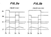
- Fig. 5 shows waveforms of various portions of the circuit shown in Fig. 4. Namely, G1 and G2 show gate signals of the switching elements 5 and 6, respectively. V1 and I1 are the voltage and current, respectively, across the reactor 9. V0 is the voltage of condenser 10 consisting the direct current output voltage. Fig. 5a shows a case in that the voltage V0 of the condenser 10 is lower than the voltage of condensers 3 and 4 and Fig. 5b shows a case in which the voltage V0 is higher than the voltage of the condensers 3 and 4 and is lower than the voltage V D of the direct current source 1.
- the power is supplied from the direct current source 1 forming an input of the device through the following route.
- a closed loop circuit is formed in the following route.
- the voltage V0 tends to increase depending on the value of the condenser 10 and the load 11.
- the voltage V0 tends to decrease. Therefore, the voltage V0 is controlled at a mean value between the maximum increased voltage and the minimum decreased voltage throughout the overall period.
- the operation mode of supplying the power from the direct current source 1 and the controlling of the voltage V0 is the same as the case of Fig. 5a.
- This system has the following advantages.
- the variation range of the input voltage is rather wide in general for instance between DC 900 ⁇ 1800 V so that device may be of a large size by an increase of the required current value to meet a large capacity load in a device having output voltages unable to be higher than the input voltages like the conventional double step-down choppers.
- the present invention is to improve the abovementioned disadvantages of the conventional devices and has its object to realize, a device of this kind being able to set the value of the output voltage freely higher or lower compared with the value of the input voltage and also the potential of the load circuit against the ground potential of the source voltage does not change stepwisely and also the device can be formed by a simple circuit arrangement in the same degree of the conventional devices.
- the circuit arrangement of the present invention is formed by connecting a first series circuit of three condensers in parallel to the input direct current voltage and also a second series circuit having a rector inserted between two switching elements is connected in parallel thereto and by connecting the both ends of the intermediate condenser with the both ends of the reactor through two diodes respectively and from the both ends of the intermediate condenser the load current is derived.
- the present invention having the abovementioned circuit realize a device of this kind able to step-up and step-down the source voltage and thus satisfying the aforementioned object of the invention.
- Figs. 1 and 2 show an essential construction and wave forms of various points of one embodiment of the present invention expressed likewisely with Figs. 4 and 5.
- 2′ and 9′ are reactors, 3′, 4′ and 10′ condensers, 5′, 6′ switching elements, 7′, 8′ diodes.
- G1′ and G2′ represent gate signals of the switching elements 5′ and 6′
- V1′ and I1′ are voltage and current of the reactor 9′
- V0′ is the voltage of the condenser 10′.
- the same parts with that in Figs. 4 and 5 are shown by the same reference numerals.
- a series circuit of a switching element 5′, a reactor 9′ and a switching element 6′ is connected to a direct current source 1 in parallel with a series circuit of condensers 3′, 10′ and 4′.
- the both ends of the condenser 10′ and that of the reactor 9′ are coupled together via diodes 7′ and 8′, respectively, as shown in the drawing and the two end terminals of the condenser 10′ are connected to a load 11.
- the condensers 3′, 4 and 10′ are of large capacities substantially not changing the voltage during one cycle of usual chopper operation.
- the voltage across the condensers 3′ and 4′ is expressed by; [(V D + V0′)/2],
- the switching element 5′ is turned-on at a time T0, a following closed circuit is formed; condenser 3′ ⁇ switching element 5′ ⁇ reactor 9′ ⁇ diode 8′ ⁇ condenser 10′ (load 11) ⁇ condenser 3′
- an increasing current will flow through the reactor 9′ having its gradient decided by the voltage of condensers 3′ and 10′ and the reactance of the reactor 9′, i.e. In this case energy is stored in the reactor 9′ while supplying a power to the load.
- direct current source 1 constituting an input of the circuit, through the following route; direct current source 1 ⁇ reactor 2′ ⁇ condenser 3′ ⁇ condenser 10′ (load 11) ⁇ condenser 4′ ⁇ direct current source 1
- the power is supplied from the direct current source 1 likewisely the previous term of (T0-T1).
- the condenser 10′ and the load 11 are supplied with power from the condenser 3′. Accordingly, depending upon the capacitance value of the condenser 10′ and the amount of the load 11, the terminal voltage V0′ of the condenser 10′, i.e. the output voltage tends to increase.
- the reactor 9′ will supply the power to the condenser 10′ and to the load 11, the said voltage V0′ tends to decrease. Namely, during the time T0 ⁇ time T1 ⁇ time T2, the voltage V0′ is controlled at an average voltage between its increased maximum voltage and decreased minimum voltage. After the time T2, a same operation is repeated by the switching element 6′ and by the condenser 4′.
- direct current source 1 ⁇ reactor 2′ ⁇ condenser 3′ ⁇ condenser 10′ (load 11) ⁇ condenser 4′ ⁇ direct current source 1
- the voltage V0′ is controlled between the increased maximum voltage and decreased minimum voltage just same as the case indicated in Fig. 2a. After the time T6, a same operation is repeated by the switching element 6′ and the condenser 4′.
- the potential of the condenser 10′ (load 11) at the side of its terminal with the diode 8′ against the negative polarity of the direct current source 1 is the same as the terminal voltage of the condenser 4′. Namely it has value of [(V D + V0′)/2] and not causing sudden stepwise variation.
- Fig. 3 shows an essential portion of an alternative embodiment of the present invention.
- 3 ⁇ , 4 ⁇ , 10 ⁇ are condensers
- 5 ⁇ , 6 ⁇ are switching elements
- 9 ⁇ is the reactor.
- the same reference numerals with that shown in Fig. 1 and Fig. 4 show the same constructive elements.
- the operation of the circuit of this modified embodiment is substantially the same with that of the previously explained embodiment.
- the polarity of the terminal voltage of the condenser 10 ⁇ is opposite to that shown in Figs. 1 and 2.
- the voltages across the condensers 3 ⁇ and 4 ⁇ are expressed by: [(V D - V0")/2] so that it is only different in that the polarity is reversed during the term of (V D ⁇ V0 ⁇ ).
- the applied voltages to the condensers 3 ⁇ and 4 ⁇ may be very small value and by using capacitors of two polarity, the device can be made more compact and light weight.
- a direct current to direct current converter being able to operate to step-up and step-down the input voltage can be realized in a simple circuit arrangement like the conventional double step down choppers.
- the potential of the load circuit against the negative terminal of the direct current source is not related to the on or off condition of the switching elements so that it does not show sudden stepwise variation and a device having a feature of generating less higher harmonic noises through its grounding capacitance.
- the operation of the two switching elements is the same as the conventional embodiments to switch alternately in mutually phase shift relationship so that the invention maintains the merit of the conventional devices.
- the switching elements are shown as GTO just as an example. But it is apparent that the invention can use other types of switching elements like transistors, FET and others.
Applications Claiming Priority (2)
| Application Number | Priority Date | Filing Date | Title |
|---|---|---|---|
| JP216857/89 | 1989-08-23 | ||
| JP1216857A JPH06103984B2 (ja) | 1989-08-23 | 1989-08-23 | 昇降圧チョッパ装置 |
Publications (3)
| Publication Number | Publication Date |
|---|---|
| EP0414465A2 true EP0414465A2 (de) | 1991-02-27 |
| EP0414465A3 EP0414465A3 (en) | 1991-03-27 |
| EP0414465B1 EP0414465B1 (de) | 1994-05-25 |
Family
ID=16694997
Family Applications (1)
| Application Number | Title | Priority Date | Filing Date |
|---|---|---|---|
| EP90309099A Expired - Lifetime EP0414465B1 (de) | 1989-08-23 | 1990-08-20 | Aufwärts und abwärts Zerhacker |
Country Status (4)
| Country | Link |
|---|---|
| US (1) | US5059887A (de) |
| EP (1) | EP0414465B1 (de) |
| JP (1) | JPH06103984B2 (de) |
| DE (1) | DE69009122T2 (de) |
Cited By (3)
| Publication number | Priority date | Publication date | Assignee | Title |
|---|---|---|---|---|
| EP2151911A1 (de) * | 2008-08-06 | 2010-02-10 | ABB Schweiz AG | DC/DC-Wandler |
| EP2176726A1 (de) * | 2007-08-08 | 2010-04-21 | Advanced Analogic Technologies, Inc. | Gleichstromrichter mit zweifacher polarität und mehreren ausgängen und spannungsregler |
| WO2010115713A3 (de) * | 2009-04-07 | 2011-03-10 | Abb Schweiz Ag | Dc/dc-wandler |
Families Citing this family (9)
| Publication number | Priority date | Publication date | Assignee | Title |
|---|---|---|---|---|
| US5208741A (en) * | 1991-03-28 | 1993-05-04 | General Electric Company | Chopper circuit for dynamic braking in an electric power conversion system |
| SE500589C2 (sv) * | 1992-10-22 | 1994-07-18 | Ericsson Telefon Ab L M | Boost-konverter med låga förluster genom begränsad backström i huvuddioden |
| US5502630A (en) * | 1994-07-19 | 1996-03-26 | Transistor Devices, Inc. | Power factor corrected rectification |
| US6002603A (en) * | 1999-02-25 | 1999-12-14 | Elliott Energy Systems, Inc. | Balanced boost/buck DC to DC converter |
| JP3888895B2 (ja) * | 2001-12-21 | 2007-03-07 | 富士通株式会社 | 正負電源発生装置および半導体装置 |
| JP5766640B2 (ja) * | 2012-03-16 | 2015-08-19 | 株式会社東芝 | 電気車制御装置 |
| CN105763056A (zh) * | 2016-02-19 | 2016-07-13 | 京东方科技集团股份有限公司 | 直流变换器 |
| CN113424423A (zh) * | 2019-02-25 | 2021-09-21 | 三菱电机株式会社 | 双降压斩波器电路 |
| TWI708472B (zh) * | 2020-03-31 | 2020-10-21 | 義守大學 | 換流裝置 |
Citations (3)
| Publication number | Priority date | Publication date | Assignee | Title |
|---|---|---|---|---|
| US3808511A (en) * | 1969-03-26 | 1974-04-30 | Nasa | Load insensitive electrical device |
| EP0060020A1 (de) * | 1981-02-27 | 1982-09-15 | The Marconi Company Limited | Gleichstromwandler |
| DE3316251A1 (de) * | 1983-05-04 | 1984-11-08 | Robert Bosch Gmbh, 7000 Stuttgart | Schaltungsanordnung zur gleichspannungswandlung |
Family Cites Families (4)
| Publication number | Priority date | Publication date | Assignee | Title |
|---|---|---|---|---|
| JPS5840913B2 (ja) * | 1978-11-16 | 1983-09-08 | 横河電機株式会社 | 一般化dc/dcコンバ−タ |
| JPS5976170A (ja) * | 1982-10-21 | 1984-05-01 | Mitsubishi Electric Corp | チヨツパ装置 |
| SU1073860A1 (ru) * | 1982-12-31 | 1984-02-15 | Киевский Ордена Ленина Политехнический Институт Им.50-Летия Великой Октябрьской Социалистической Революции | Двухканальный преобразователь напр жени |
| US4622511A (en) * | 1985-04-01 | 1986-11-11 | Raytheon Company | Switching regulator |
-
1989
- 1989-08-23 JP JP1216857A patent/JPH06103984B2/ja not_active Expired - Fee Related
-
1990
- 1990-08-10 US US07/566,085 patent/US5059887A/en not_active Expired - Fee Related
- 1990-08-20 DE DE69009122T patent/DE69009122T2/de not_active Expired - Fee Related
- 1990-08-20 EP EP90309099A patent/EP0414465B1/de not_active Expired - Lifetime
Patent Citations (3)
| Publication number | Priority date | Publication date | Assignee | Title |
|---|---|---|---|---|
| US3808511A (en) * | 1969-03-26 | 1974-04-30 | Nasa | Load insensitive electrical device |
| EP0060020A1 (de) * | 1981-02-27 | 1982-09-15 | The Marconi Company Limited | Gleichstromwandler |
| DE3316251A1 (de) * | 1983-05-04 | 1984-11-08 | Robert Bosch Gmbh, 7000 Stuttgart | Schaltungsanordnung zur gleichspannungswandlung |
Cited By (4)
| Publication number | Priority date | Publication date | Assignee | Title |
|---|---|---|---|---|
| EP2176726A1 (de) * | 2007-08-08 | 2010-04-21 | Advanced Analogic Technologies, Inc. | Gleichstromrichter mit zweifacher polarität und mehreren ausgängen und spannungsregler |
| EP2176726A4 (de) * | 2007-08-08 | 2011-10-19 | Advanced Analogic Tech Inc | Gleichstromrichter mit zweifacher polarität und mehreren ausgängen und spannungsregler |
| EP2151911A1 (de) * | 2008-08-06 | 2010-02-10 | ABB Schweiz AG | DC/DC-Wandler |
| WO2010115713A3 (de) * | 2009-04-07 | 2011-03-10 | Abb Schweiz Ag | Dc/dc-wandler |
Also Published As
| Publication number | Publication date |
|---|---|
| EP0414465B1 (de) | 1994-05-25 |
| US5059887A (en) | 1991-10-22 |
| EP0414465A3 (en) | 1991-03-27 |
| DE69009122T2 (de) | 1994-10-13 |
| JPH0382364A (ja) | 1991-04-08 |
| DE69009122D1 (de) | 1994-06-30 |
| JPH06103984B2 (ja) | 1994-12-14 |
Similar Documents
| Publication | Publication Date | Title |
|---|---|---|
| US5204809A (en) | H-driver DC-to-DC converter utilizing mutual inductance | |
| US4720667A (en) | Zero-current switching quasi-resonant converters operating in a full-wave mode | |
| EP0508664B1 (de) | Gleichspannungswandler | |
| US5510974A (en) | High frequency push-pull converter with input power factor correction | |
| US5543704A (en) | Pulse width modulated DC-to-DC boost converter | |
| US5761055A (en) | Driving pulse output limiting circuit | |
| JP3164838B2 (ja) | スイッチング回路及びそれを用いた変換装置、力率改善電源装置 | |
| EP0414465B1 (de) | Aufwärts und abwärts Zerhacker | |
| US4513361A (en) | Multi-phase DC-to-AC and DC-to-DC boost converter | |
| US5075836A (en) | Series resonant power converter | |
| US5644479A (en) | Switching power supply device | |
| US5486994A (en) | Device for control of the oscillating circuit of a voltage inverter operating under quasi-resonance with pulse modulation regulation | |
| US6590786B2 (en) | System for controlling the delivery of power to DC computer components utilizing phase shift regulation | |
| Koizumi et al. | Resonant DC/DC converter with class DE inverter and class E rectifier using thinned-out method (deleting some of the pulses to the rectifier) | |
| US5229930A (en) | Welding inverter and method for controlling a welding inverter | |
| JPH07274532A (ja) | 低電圧のもとでスイッチングが行えるように構成されたチョッパ式電源 | |
| EP0230358A3 (de) | Radiofrequenzhochspannungsleistungsversorgung | |
| US5014182A (en) | High frequency self-oscillating inverter with negligible switching losses | |
| US5923155A (en) | Circuit for the production of an auxiliary voltage | |
| US20030076699A1 (en) | Half-bridge converter with high power factor | |
| JPH0327768A (ja) | 共振形dc―dcコンバータの制御方法 | |
| JPH08168240A (ja) | Dc−dcコンバータ | |
| JP2614056B2 (ja) | Dc/dcコンバータ | |
| SU1201977A1 (ru) | Импульсный преобразователь посто нного напр жени | |
| RU1791929C (ru) | Стабилизированный преобразователь |
Legal Events
| Date | Code | Title | Description |
|---|---|---|---|
| PUAI | Public reference made under article 153(3) epc to a published international application that has entered the european phase |
Free format text: ORIGINAL CODE: 0009012 |
|
| PUAL | Search report despatched |
Free format text: ORIGINAL CODE: 0009013 |
|
| AK | Designated contracting states |
Kind code of ref document: A2 Designated state(s): CH DE FR GB LI SE |
|
| AK | Designated contracting states |
Kind code of ref document: A3 Designated state(s): CH DE FR GB LI SE |
|
| 17P | Request for examination filed |
Effective date: 19910430 |
|
| 17Q | First examination report despatched |
Effective date: 19930420 |
|
| GRAA | (expected) grant |
Free format text: ORIGINAL CODE: 0009210 |
|
| AK | Designated contracting states |
Kind code of ref document: B1 Designated state(s): CH DE FR GB LI SE |
|
| REF | Corresponds to: |
Ref document number: 69009122 Country of ref document: DE Date of ref document: 19940630 |
|
| ET | Fr: translation filed | ||
| EAL | Se: european patent in force in sweden |
Ref document number: 90309099.1 |
|
| PLBE | No opposition filed within time limit |
Free format text: ORIGINAL CODE: 0009261 |
|
| STAA | Information on the status of an ep patent application or granted ep patent |
Free format text: STATUS: NO OPPOSITION FILED WITHIN TIME LIMIT |
|
| 26N | No opposition filed | ||
| PGFP | Annual fee paid to national office [announced via postgrant information from national office to epo] |
Ref country code: GB Payment date: 19960808 Year of fee payment: 7 |
|
| PGFP | Annual fee paid to national office [announced via postgrant information from national office to epo] |
Ref country code: CH Payment date: 19960812 Year of fee payment: 7 |
|
| PGFP | Annual fee paid to national office [announced via postgrant information from national office to epo] |
Ref country code: SE Payment date: 19960815 Year of fee payment: 7 |
|
| PGFP | Annual fee paid to national office [announced via postgrant information from national office to epo] |
Ref country code: FR Payment date: 19960828 Year of fee payment: 7 |
|
| PGFP | Annual fee paid to national office [announced via postgrant information from national office to epo] |
Ref country code: DE Payment date: 19960930 Year of fee payment: 7 |
|
| PG25 | Lapsed in a contracting state [announced via postgrant information from national office to epo] |
Ref country code: GB Free format text: LAPSE BECAUSE OF NON-PAYMENT OF DUE FEES Effective date: 19970820 |
|
| PG25 | Lapsed in a contracting state [announced via postgrant information from national office to epo] |
Ref country code: SE Free format text: LAPSE BECAUSE OF NON-PAYMENT OF DUE FEES Effective date: 19970821 |
|
| PG25 | Lapsed in a contracting state [announced via postgrant information from national office to epo] |
Ref country code: LI Free format text: LAPSE BECAUSE OF NON-PAYMENT OF DUE FEES Effective date: 19970831 Ref country code: CH Free format text: LAPSE BECAUSE OF NON-PAYMENT OF DUE FEES Effective date: 19970831 |
|
| GBPC | Gb: european patent ceased through non-payment of renewal fee |
Effective date: 19970820 |
|
| REG | Reference to a national code |
Ref country code: CH Ref legal event code: PL |
|
| PG25 | Lapsed in a contracting state [announced via postgrant information from national office to epo] |
Ref country code: FR Free format text: LAPSE BECAUSE OF NON-PAYMENT OF DUE FEES Effective date: 19980430 |
|
| PG25 | Lapsed in a contracting state [announced via postgrant information from national office to epo] |
Ref country code: DE Free format text: LAPSE BECAUSE OF NON-PAYMENT OF DUE FEES Effective date: 19980501 |
|
| EUG | Se: european patent has lapsed |
Ref document number: 90309099.1 |
|
| REG | Reference to a national code |
Ref country code: FR Ref legal event code: ST |