EP0413451B1 - Packung von Halbleiterchips - Google Patents
Packung von Halbleiterchips Download PDFInfo
- Publication number
- EP0413451B1 EP0413451B1 EP90308151A EP90308151A EP0413451B1 EP 0413451 B1 EP0413451 B1 EP 0413451B1 EP 90308151 A EP90308151 A EP 90308151A EP 90308151 A EP90308151 A EP 90308151A EP 0413451 B1 EP0413451 B1 EP 0413451B1
- Authority
- EP
- European Patent Office
- Prior art keywords
- package
- printed circuit
- chip
- electroconductive
- semiconductor chip
- Prior art date
- Legal status (The legal status is an assumption and is not a legal conclusion. Google has not performed a legal analysis and makes no representation as to the accuracy of the status listed.)
- Expired - Lifetime
Links
Images
Classifications
-
- H—ELECTRICITY
- H10—SEMICONDUCTOR DEVICES; ELECTRIC SOLID-STATE DEVICES NOT OTHERWISE PROVIDED FOR
- H10P—GENERIC PROCESSES OR APPARATUS FOR THE MANUFACTURE OR TREATMENT OF DEVICES COVERED BY CLASS H10
- H10P74/00—Testing or measuring during manufacture or treatment of wafers, substrates or devices
- H10P74/27—Structural arrangements therefor
- H10P74/273—Interconnections for measuring or testing, e.g. probe pads
-
- H—ELECTRICITY
- H10—SEMICONDUCTOR DEVICES; ELECTRIC SOLID-STATE DEVICES NOT OTHERWISE PROVIDED FOR
- H10P—GENERIC PROCESSES OR APPARATUS FOR THE MANUFACTURE OR TREATMENT OF DEVICES COVERED BY CLASS H10
- H10P74/00—Testing or measuring during manufacture or treatment of wafers, substrates or devices
- H10P74/23—Testing or measuring during manufacture or treatment of wafers, substrates or devices characterised by multiple measurements, corrections, marking or sorting processes
-
- H—ELECTRICITY
- H10—SEMICONDUCTOR DEVICES; ELECTRIC SOLID-STATE DEVICES NOT OTHERWISE PROVIDED FOR
- H10W—GENERIC PACKAGES, INTERCONNECTIONS, CONNECTORS OR OTHER CONSTRUCTIONAL DETAILS OF DEVICES COVERED BY CLASS H10
- H10W70/00—Package substrates; Interposers; Redistribution layers [RDL]
- H10W70/60—Insulating or insulated package substrates; Interposers; Redistribution layers
-
- H—ELECTRICITY
- H10—SEMICONDUCTOR DEVICES; ELECTRIC SOLID-STATE DEVICES NOT OTHERWISE PROVIDED FOR
- H10W—GENERIC PACKAGES, INTERCONNECTIONS, CONNECTORS OR OTHER CONSTRUCTIONAL DETAILS OF DEVICES COVERED BY CLASS H10
- H10W76/00—Containers; Fillings or auxiliary members therefor; Seals
- H10W76/10—Containers or parts thereof
- H10W76/12—Containers or parts thereof characterised by their shape
- H10W76/15—Containers comprising an insulating or insulated base
- H10W76/157—Containers comprising an insulating or insulated base having interconnections parallel to the insulating or insulated base
-
- H—ELECTRICITY
- H10—SEMICONDUCTOR DEVICES; ELECTRIC SOLID-STATE DEVICES NOT OTHERWISE PROVIDED FOR
- H10W—GENERIC PACKAGES, INTERCONNECTIONS, CONNECTORS OR OTHER CONSTRUCTIONAL DETAILS OF DEVICES COVERED BY CLASS H10
- H10W90/00—Package configurations
-
- H—ELECTRICITY
- H10—SEMICONDUCTOR DEVICES; ELECTRIC SOLID-STATE DEVICES NOT OTHERWISE PROVIDED FOR
- H10W—GENERIC PACKAGES, INTERCONNECTIONS, CONNECTORS OR OTHER CONSTRUCTIONAL DETAILS OF DEVICES COVERED BY CLASS H10
- H10W72/00—Interconnections or connectors in packages
- H10W72/50—Bond wires
- H10W72/541—Dispositions of bond wires
- H10W72/5449—Dispositions of bond wires not being orthogonal to a side surface of the chip, e.g. fan-out arrangements
-
- H—ELECTRICITY
- H10—SEMICONDUCTOR DEVICES; ELECTRIC SOLID-STATE DEVICES NOT OTHERWISE PROVIDED FOR
- H10W—GENERIC PACKAGES, INTERCONNECTIONS, CONNECTORS OR OTHER CONSTRUCTIONAL DETAILS OF DEVICES COVERED BY CLASS H10
- H10W90/00—Package configurations
- H10W90/701—Package configurations characterised by the relative positions of pads or connectors relative to package parts
- H10W90/751—Package configurations characterised by the relative positions of pads or connectors relative to package parts of bond wires
- H10W90/754—Package configurations characterised by the relative positions of pads or connectors relative to package parts of bond wires between a chip and a stacked insulating package substrate, interposer or RDL
Definitions
- US-A-3780352 discloses a semiconductor device having the features of the pre-characterising portion of claim 1.
- RAM packages A number of known RAM packages exist. For example it is known to have dual-inline-packages (DIPs), zig-zag-packages (ZIP), surface mount packages (SOIC or SOJ) and the so-called "flip-chip" dies. Particular examples of such packages can achieve a packing density of silicon area over printed circuit board area of above 25%, the density normally achieved only with hybrid packaging techniques which mix thin or thick film and printed circuit technologies.
- DIPs dual-inline-packages
- ZIP zig-zag-packages
- SOIC or SOJ surface mount packages
- SOIC flip-chip
- the thickness is necessary partly to turn the leads under the body and also partly to give enough thickness of plastics material used for the package to give the package mechanical strength.
- a so-called "VSOP" single RAM chip has been produced by Mitsubishi which is very small, has short leads on a fine pitch at the ends of the package and is only lmm thick.
- the VSOP package is so small that many RAM chips are too large to fit into it. Also, it has such a small surface area that heat dissipation from the package is lower than for a larger package, although a benefit from the thinness is that there is a very short thermal path between the chip and the outside surface of the package.
- the present invention provides a semiconductor device comprising at least one semiconductor chip, the or each semiconductor chip having a plurality of chip bonding pads, a package which encloses the at least one semiconductor chip, a first level interconnect which extends externally of the package to provide a plurality of outer leads, and a second level interconnect comprising means for electrically connecting the chip bonding pads to selected contacts on the first level interconnect, which contacts overlie the at least one semiconductor chip, characterised in that the first level interconnect comprises a printed circuit which overlies the at least one semiconductor chip in the package and comprises a plurality of electroconductive tracks disposed between two layers of insulating material, the plurality of electroconductive tracks extending between opposed rows of outer leads on respective opposed ends of the printed circuit, one of said two layers of insulating material which is remote from the or each semiconductor chip either having holes therein which reveal the said contacts which comprise bonding pads of the electroconductive tracks, or having a plurality of electroconductive vias of the electroconductive tracks extending therethrough to comprise the contacts, and the means for electrical
- the semiconductor device comprises a plurality of random access memory chips.
- the present invention is not limited to the packaging of memory chips.
- outer leads 12 for connection to a printed circuit board (not shown) on which the package is to be mounted, the outer leads 12 being formed by exposure of the electroconductive tracks 20 in the flexible printed circuit 8.
- a lid 14 overlies the flexible printed circuit 8 and has the same dimensions as the base 6.
- the base 6 and lid 14 have peripheral flanges which are provided with complementary registration pegs and holes 16, 18 which enable the base and lid 6, 14 accurately to be located in registry with each other thereby to form a sealed package 2.
- the base 6 and lid 14 are adhered together e.g. by a silicone adhesive along their peripheral mating surfaces so as to seal the package.
- the inner volume of the package 2 may include a material (not shown) which covers the electrical connections in the package and provides protection from moisture penetration of the chips.
- a material may be, for example a conventional moulding material, a "glob top” epoxy as used in known hybrid packages or a self-healing gel contained by a non-hermetic enclosure.
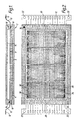
- a row of twenty outer leads is provided at each end of the printed circuit.
- Each end 10 of the flexible printed circuit 8 is also provided with registration holes 22 to enable the outer leads 12 accurately to be registered onto respective contacts on a printed circuit board (not shown).
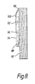
- the flexible circuit 8 as described above, comprises the electroconductive tracks 20 which are sandwiched between a lower insulating layer 24 which is between the tracks 20 and the chips 4 and an upper insulating layer 26 which covers the tracks 20.
- the upper insulating layer 26 is provided with a number of openings 28 each of which exposes a respective bonding pad 30.
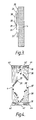
- the ends 32, 34 of each chip 4 are each provided, in known manner, with a row of chip bonding pads 36.
- three partially-overlapping rectangular holes 40, 42, 44 are cut in the insulating layers 24, 26 of the flexible circuit 8 at a location overlying each row of chip bonding pads 36.
- This enables the bond wires 38 to extend upwardly through the holes 40, 42, 44 from the chip bonding pads 36 thereby to extend over the upper surface of the flexible printed circuit 8 and connect with the respective bonding pads 30.
- there may be provided a group of spaced holes or slots overlying the chip bonding pads. This gives a mechanically more stable flexible printed circuit.
- spaced holes are required when the invention is employed to package an integrated circuit having chip bonding pads on all four of its sides.
- Figure 5 shows schematically the layout of a portion of an elongate strip 45 including the thin flexible printed circuit 8 prior to connection to the chips 4. For clarity of illustration, any holes which are cut in the thin printed circuit are not shown. However, the printed circuit may be provided with registration holes to allow registration of the thin printed circuit relative to the base of the package.
- the strip consists of a central region 46 comprising the tracks 20 and the bonding pads 30.
- the strip 45 also includes the outer leads 12 at opposed ends of the central region 46. Connected to the outer leads 12 at opposed ends of the portion of the strip 45 are opposed regions of test circuitry 48 which are employed, when the flexible printed circuit 8 has been connected to the chips 4 by the bond wires 38, to test the operation of the packaged semiconductor device.
- the central region 46 also includes opposed, longitudinally directed regions 50 of copper which act mechanically to support the central region 46.
- the central and test regions 46, 48 are bounded on opposed transverse sides by lateral supporting regions 54 which are provided with rows of tractor feed holes 56 which enable the flexible printed circuit 8 to be fed along a production line in a continuous manufacturing process.
- lateral supporting regions 54 which are provided with rows of tractor feed holes 56 which enable the flexible printed circuit 8 to be fed along a production line in a continuous manufacturing process.
- tractor feed holes 56 which enable the flexible printed circuit 8 to be fed along a production line in a continuous manufacturing process.
- the test regions 48 and the lateral supporting regions 54 of the strip are removed so that the final flexible printed circuit 8 is as shown in Figure 2.
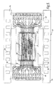
- FIGS 6 to 8 illustrate a semiconductor chip package in accordance with a second embodiment of the present invention.
- a semiconductor package 70 consists of a base 72 e.g. of metal to which is adhered a row of semiconductor chips 74. In the illustrated embodiment, there is a row of four RAM chips 74.
- a flexible printed circuit 76 overlies the row of chips 74.
- the flexible printed circuit 76 is carried by a rectangular supporting member 78 which, in the package 70, constitutes a peripheral side wall of the package 70.
- a lid 80 overlies the side wall 78 and the base 72. The base 72 and the lid 80 are sealingly adhered to the side wall 78 thereby to seal the chips 74 inside the package 70.
- a material (not shown) for protecting the chips from moisture may be incorporated in the package 70.
- the insulated layers 88, 94 of the flexible printed circuit 76 are provided with holes in registry with the chip bonding pads 98, the holes being similar to the holes 40, 42, 44 provided in the first embodiment.
- Figure 7 shows schematically the connections made between the tracks 92 and the chip bonding pads 98 although it will of course be understood that the TAB inner leads do not require the thin wire-like connectors shown schematically in Figure 7 but rather they consist of narrow strips so as to have sufficient mechanical strength at the ends thereof which are to be bonded to the chip bond pads 98.
- the insulating material 88, 94 of the flexible printed circuit 76 extends fully across the width of the package so as to provide increased mechanical strength for the flexible printed circuit 76.
- the underside of each of the chips is adhered to a thermally conductive sheet constituting the base of the package.
- the sheet spreads the heat out between the chips so that all the chips are within a few degrees of the same temperature.
- the sheet also provides and exceptionally short thermal path to the external surface of the package.
- Particular preferred materials for the thermally conductive sheet are metals which also give excellent mechanical strength, thereby providing a mechanically sound package which is thinner than would be possible using standard package plastics.
- the base of the package may be made of aluminium having a thickness of around 0.038 cm. The thermally conductive sheet constituting the base is actually treated as the top of the package when the package is assembled onto a printed circuit board.
- This orientation of the package also puts the outer leads of the thin printed circuit in the right orientation so that they can be soldered to the printed circuit board without removing the insulating laminate of the thin printed circuit. This keeps the package leads in exact register with respect to each other and overcomes the problems of the fragility of conventional package leads. Furthermore, since a number of chips are assembled in a single package, this means that the package is large enough to dissipate the heat generated by the chips. Normally, the circuitry would be arranged so that only one or two of the chips in the package is or are active at any given time, thus providing that for the one or two active chips, an effective heat sink capability of four chips is available.
- the chips are connected to each other and to external leads by a thin printed circuit which lies over the active circuitry on the chip.
- 96 leads would be required by an assembly of four RAMs consisting of four separate 24 lead packages whereas in the present invention a single package containing four RAMs would require only 32 leads.
- the reduction in the number of leads provides a gain in reliability when compared to the prior art since a reduced number of soldered joints on the board is employed using the multi-chip RAM packages of the present invention.
- the illustrated embodiments respectively employ bonding wires and tape-automated-bonding (TAB) tape to form a second level of interconnect which is separated from the first level of interconnect, constituted by the tracks of the printed circuit on an insulating layer, by an insulating layer.
- TAB tape-automated-bonding
- the use of conventional bonding wires reduces the cost of the semiconductor package.
- Such plated through holes if used to connect to tracks acting in place of the bond wires, would need to be on a pitch of about 0.02cm, which, while possible, is not inexpensive.
Landscapes
- Semiconductor Memories (AREA)
- Wire Bonding (AREA)
Claims (6)
- Halbleiterbauelement (2) aufweisend wenigstens einen Haltleiterchip (4), wobei der oder jeder Halbleiterchip (4) eine Mehrzahl von Chip-Bondanschlüssen (36) aufweist, ein Gehäuse (6,14), welches den wenigstens einen Halbleiterchip (4) umgibt, eine Erstniveau-Zwischenverbindung, welche sich vom Gehäuse (6,14) nach außen erstreckt und mehrere äußere Anschlüsse (12) bereitstellt, und eine Zweitniveau-Zwischenverbindung mit Mittel (38) zum elektrischen Verbinden der Chip-Bondanschlüsse (36) mit ausgewählten Kontakten (30) auf der Erstniveau-Zwischenverbindung, wobei die Kontakte (30) über dem wenigstens einen Halbleiterchip (4) liegen, dadurch gekennzeichnet, daß die Zweitniveau-Zwischenverbindung über der Erstniveau-Zwischenverbindung angeordnet ist, wobei die Erstniveau-Zwischenverbindung eine gedruckte Schaltung (8) aufweist, welche über dem wenigstens einen Halbleiterchip (4) im Gehäuse (6,14) liegt und eine Mehrzahl von Leiterbahnen (20) aufweist, die zwischen zwei Schichten (24,26) von isolierendem Material angeordnet sind, wobei die Mehrzahl der Leiterbahnen (20) sich zwischen gegenüberliegenden Reihen von äußeren Anschlüssen an jeweils gegenüberliegenden Enden der gedruckten Schaltung (8) erstrecken, wobei eine der zwei Schichten von isolierendem Material (26), welche von dem oder jedem Halbleiterchip (4) beabstandet ist, entweder Durchbrüche (28), welche die Kontakte (30) freilegen, die Bondanschlüsse der Leiterbahnen (30) enthalten, oder eine Mehrzahl von leitenden Verbindungskontakten (96) der Leiterbahnen (92) aufweist, welche sich durch diese hindurch erstrecken und die Kontakte (30) aufweisen, und wobei das Mittel zum elektrischen Verbinden jeweils entweder eine Mehrzahl von Bonddrähten (38), die sich jeweils oberhalb einer Schicht des isolierenden Materials (26) erstrecken und einen jeweiligen Bondanschluß (30) mit einem jeweiligen Chip-Bondanschluß (36) verbinden, oder eine Matrix von leitenden Anschlüssen (100) umfaßt, die sich jeweils oberhalb der Schicht von isolierendem Material (94) erstrecken und einen jeweiligen Verbindungskontakt (96) mit einem jeweiligen Chip-Bondanschluß (98) verbinden.
- Halbleiterbauelement nach Anspruch 1, bei welchem das Mittel zum elektrischen Verbinden innerhalb des Bereiches des wenigstens einen Halbleiterchips (4) angeordnet ist.
- Halbleiterbauelement nach Anspruch 1 oder Anspruch 2, welches eine Mehrzahl von Schreib/Lese-Speicherchips (RAMs) umfaßt.
- Halbleiterbauelement nach einem der Ansprüche 1 bis 3, bei welchem die gedruckte Schaltung (8) flexibel ist.
- Halbleiterbauelement nach einem der vorstehenden Ansprüche, bei welchem die leitenden Anschlüsse (100) aus einem Tape-Automated-Bonded (TAB) Band gebildet sind.
- Halbleiterbauelement (2) nach einem der vorstehenden Ansprüche, bei welchem die gedruckte Schaltung (8) eine Mehrzahl von Ausrichtungslöchern (22) enthält, welche außerhalb des Gehäuses (6,14) angeordnet sind, so daß die äußeren Anschlüsse (12) auf einer gedruckten Schaltungsplatte ausgerichtet werden können.
Applications Claiming Priority (2)
| Application Number | Priority Date | Filing Date | Title |
|---|---|---|---|
| GB8918482 | 1989-08-14 | ||
| GB898918482A GB8918482D0 (en) | 1989-08-14 | 1989-08-14 | Packaging semiconductor chips |
Publications (3)
| Publication Number | Publication Date |
|---|---|
| EP0413451A2 EP0413451A2 (de) | 1991-02-20 |
| EP0413451A3 EP0413451A3 (en) | 1991-09-04 |
| EP0413451B1 true EP0413451B1 (de) | 2002-01-30 |
Family
ID=10661580
Family Applications (1)
| Application Number | Title | Priority Date | Filing Date |
|---|---|---|---|
| EP90308151A Expired - Lifetime EP0413451B1 (de) | 1989-08-14 | 1990-07-25 | Packung von Halbleiterchips |
Country Status (5)
| Country | Link |
|---|---|
| US (2) | US5073816A (de) |
| EP (1) | EP0413451B1 (de) |
| JP (1) | JP3066048B2 (de) |
| DE (1) | DE69033909D1 (de) |
| GB (1) | GB8918482D0 (de) |
Cited By (1)
| Publication number | Priority date | Publication date | Assignee | Title |
|---|---|---|---|---|
| US7098078B2 (en) | 1990-09-24 | 2006-08-29 | Tessera, Inc. | Microelectronic component and assembly having leads with offset portions |
Families Citing this family (38)
| Publication number | Priority date | Publication date | Assignee | Title |
|---|---|---|---|---|
| GB8918482D0 (en) * | 1989-08-14 | 1989-09-20 | Inmos Ltd | Packaging semiconductor chips |
| US5148265A (en) * | 1990-09-24 | 1992-09-15 | Ist Associates, Inc. | Semiconductor chip assemblies with fan-in leads |
| US5679977A (en) * | 1990-09-24 | 1997-10-21 | Tessera, Inc. | Semiconductor chip assemblies, methods of making same and components for same |
| US5148266A (en) * | 1990-09-24 | 1992-09-15 | Ist Associates, Inc. | Semiconductor chip assemblies having interposer and flexible lead |
| US5774220A (en) * | 1990-11-20 | 1998-06-30 | Mesacon Gesellschaft Fur Messtechnik Mbh | Continuous contactless measurement of profiles and apparatus for carrying out the measurement process |
| JP2925337B2 (ja) * | 1990-12-27 | 1999-07-28 | 株式会社東芝 | 半導体装置 |
| EP0494782B1 (de) * | 1991-01-11 | 1997-04-23 | Texas Instruments Incorporated | Prüf- und Einbrennsystem für einen Wafer und Methode für deren Herstellung |
| JP2960560B2 (ja) * | 1991-02-28 | 1999-10-06 | 株式会社日立製作所 | 超小型電子機器 |
| JPH0821807B2 (ja) * | 1993-04-07 | 1996-03-04 | 日本電気株式会社 | マイクロ波回路モジュールの製造装置 |
| FR2720190B1 (fr) * | 1994-05-20 | 1996-08-02 | Matra Marconi Space France | Procédé de raccordement des plages de sortie d'une puce à circuit intégré, et module multipuces ainsi obtenu. |
| US6223146B1 (en) * | 1994-06-29 | 2001-04-24 | Kelsey-Hayes Company | Method and apparatus for manufacturing a programmed electronic control unit for use in an anti-lock braking (ABS) system |
| GB2291715A (en) * | 1995-04-26 | 1996-01-31 | Memory Corp Plc | Improved test and assembly apparatus |
| US5744870A (en) | 1996-06-07 | 1998-04-28 | Micron Technology, Inc. | Memory device with multiple input/output connections |
| US5942798A (en) * | 1997-11-24 | 1999-08-24 | Stmicroelectronics, Inc. | Apparatus and method for automating the underfill of flip-chip devices |
| US5936877A (en) * | 1998-02-13 | 1999-08-10 | Micron Technology, Inc. | Die architecture accommodating high-speed semiconductor devices |
| US6429528B1 (en) * | 1998-02-27 | 2002-08-06 | Micron Technology, Inc. | Multichip semiconductor package |
| US6111756A (en) * | 1998-09-11 | 2000-08-29 | Fujitsu Limited | Universal multichip interconnect systems |
| JP3847997B2 (ja) * | 1999-01-22 | 2006-11-22 | 東芝マイクロエレクトロニクス株式会社 | 半導体装置及び両面mcpチップ |
| JP3360723B2 (ja) * | 1999-06-08 | 2002-12-24 | 日本電気株式会社 | 半導体素子のチップサイズパッケージ |
| US6351144B1 (en) * | 1999-07-15 | 2002-02-26 | Altera Corporation | Programmable logic device with unified cell structure including signal interface bumps |
| US6429028B1 (en) | 2000-08-29 | 2002-08-06 | Dpa Labs, Incorporated | Process to remove semiconductor chips from a plastic package |
| US6870276B1 (en) | 2001-12-26 | 2005-03-22 | Micron Technology, Inc. | Apparatus for supporting microelectronic substrates |
| US6900531B2 (en) * | 2002-10-25 | 2005-05-31 | Freescale Semiconductor, Inc. | Image sensor device |
| US7550842B2 (en) | 2002-12-12 | 2009-06-23 | Formfactor, Inc. | Integrated circuit assembly |
| US6982566B1 (en) * | 2004-04-01 | 2006-01-03 | Altera Corporation | Method and apparatus for operating a burn-in board to achieve lower equilibrium temperature and to minimize thermal runaway |
| US7701042B2 (en) * | 2006-09-18 | 2010-04-20 | Stats Chippac Ltd. | Integrated circuit package system for chip on lead |
| KR20090021605A (ko) * | 2007-08-27 | 2009-03-04 | 삼성전기주식회사 | 반도체 메모리 패키지 |
| US10177054B2 (en) | 2011-10-27 | 2019-01-08 | Global Circuit Innovations, Inc. | Method for remapping a packaged extracted die |
| US10002846B2 (en) | 2011-10-27 | 2018-06-19 | Global Circuit Innovations Incorporated | Method for remapping a packaged extracted die with 3D printed bond connections |
| US10128161B2 (en) | 2011-10-27 | 2018-11-13 | Global Circuit Innovations, Inc. | 3D printed hermetic package assembly and method |
| US9966319B1 (en) | 2011-10-27 | 2018-05-08 | Global Circuit Innovations Incorporated | Environmental hardening integrated circuit method and apparatus |
| US10147660B2 (en) | 2011-10-27 | 2018-12-04 | Global Circuits Innovations, Inc. | Remapped packaged extracted die with 3D printed bond connections |
| US9870968B2 (en) | 2011-10-27 | 2018-01-16 | Global Circuit Innovations Incorporated | Repackaged integrated circuit and assembly method |
| US9935028B2 (en) * | 2013-03-05 | 2018-04-03 | Global Circuit Innovations Incorporated | Method and apparatus for printing integrated circuit bond connections |
| US10109606B2 (en) | 2011-10-27 | 2018-10-23 | Global Circuit Innovations, Inc. | Remapped packaged extracted die |
| US10115645B1 (en) | 2018-01-09 | 2018-10-30 | Global Circuit Innovations, Inc. | Repackaged reconditioned die method and assembly |
| US11181570B2 (en) | 2018-06-15 | 2021-11-23 | Rosemount Inc. | Partial discharge synthesizer |
| US11508680B2 (en) | 2020-11-13 | 2022-11-22 | Global Circuit Innovations Inc. | Solder ball application for singular die |
Citations (2)
| Publication number | Priority date | Publication date | Assignee | Title |
|---|---|---|---|---|
| EP0198194A1 (de) * | 1985-04-18 | 1986-10-22 | International Business Machines Corporation | Halbleiterelement in einem Gehäuse |
| EP0329317A2 (de) * | 1988-02-12 | 1989-08-23 | Hitachi, Ltd. | Halbleiteranordnung mit einer isolierenden Folie |
Family Cites Families (20)
| Publication number | Priority date | Publication date | Assignee | Title |
|---|---|---|---|---|
| US3780352A (en) * | 1968-06-25 | 1973-12-18 | J Redwanz | Semiconductor interconnecting system using conductive patterns bonded to thin flexible insulating films |
| US3684818A (en) * | 1970-10-20 | 1972-08-15 | Sprague Electric Co | Multi-layer beam-lead wiring for semiconductor packages |
| KR900001273B1 (ko) * | 1983-12-23 | 1990-03-05 | 후지쑤 가부시끼가이샤 | 반도체 집적회로 장치 |
| JPS61111561A (ja) * | 1984-10-05 | 1986-05-29 | Fujitsu Ltd | 半導体装置 |
| US4903120A (en) * | 1985-11-22 | 1990-02-20 | Texas Instruments Incorporated | Chip carrier with interconnects on lid |
| US4890152A (en) * | 1986-02-14 | 1989-12-26 | Matsushita Electric Works, Ltd. | Plastic molded chip carrier package and method of fabricating the same |
| US4890153A (en) * | 1986-04-04 | 1989-12-26 | Fairchild Semiconductor Corporation | Single bonding shelf, multi-row wire-bond finger layout for integrated circuit package |
| EP0305398B1 (de) * | 1986-05-01 | 1991-09-25 | Honeywell Inc. | Verbindungsanordnung für mehrere integrierte schaltungen |
| EP0268181B1 (de) * | 1986-11-15 | 1992-07-29 | Matsushita Electric Works, Ltd. | Gegossenes Kunststoff-Chip-Gehäuse mit Steckermuster |
| US4953005A (en) * | 1987-04-17 | 1990-08-28 | Xoc Devices, Inc. | Packaging system for stacking integrated circuits |
| US4914741A (en) * | 1987-06-08 | 1990-04-03 | Digital Equipment Corporation | Tape automated bonding semiconductor package |
| JP2507476B2 (ja) * | 1987-09-28 | 1996-06-12 | 株式会社東芝 | 半導体集積回路装置 |
| GB2218847B (en) * | 1988-05-16 | 1991-04-24 | Gen Electric Co Plc | Carrier for semiconductor devices |
| IL90601A0 (en) * | 1988-06-24 | 1990-01-18 | Unistructure Inc | Protected lead frames for inter-connecting semiconductor devices and their fabrication |
| US4939570A (en) * | 1988-07-25 | 1990-07-03 | International Business Machines, Corp. | High power, pluggable tape automated bonding package |
| JPH02174255A (ja) * | 1988-12-27 | 1990-07-05 | Mitsubishi Electric Corp | 半導体集積回路装置 |
| US4912547A (en) * | 1989-01-30 | 1990-03-27 | International Business Machines Corporation | Tape bonded semiconductor device |
| GB8918482D0 (en) * | 1989-08-14 | 1989-09-20 | Inmos Ltd | Packaging semiconductor chips |
| US5045921A (en) * | 1989-12-26 | 1991-09-03 | Motorola, Inc. | Pad array carrier IC device using flexible tape |
| US5018005A (en) * | 1989-12-27 | 1991-05-21 | Motorola Inc. | Thin, molded, surface mount electronic device |
-
1989
- 1989-08-14 GB GB898918482A patent/GB8918482D0/en active Pending
-
1990
- 1990-07-25 DE DE69033909T patent/DE69033909D1/de not_active Expired - Lifetime
- 1990-07-25 EP EP90308151A patent/EP0413451B1/de not_active Expired - Lifetime
- 1990-07-25 US US07/557,940 patent/US5073816A/en not_active Expired - Lifetime
- 1990-08-08 JP JP2210119A patent/JP3066048B2/ja not_active Expired - Lifetime
-
1994
- 1994-10-21 US US08/327,447 patent/US6100581A/en not_active Expired - Lifetime
Patent Citations (2)
| Publication number | Priority date | Publication date | Assignee | Title |
|---|---|---|---|---|
| EP0198194A1 (de) * | 1985-04-18 | 1986-10-22 | International Business Machines Corporation | Halbleiterelement in einem Gehäuse |
| EP0329317A2 (de) * | 1988-02-12 | 1989-08-23 | Hitachi, Ltd. | Halbleiteranordnung mit einer isolierenden Folie |
Cited By (4)
| Publication number | Priority date | Publication date | Assignee | Title |
|---|---|---|---|---|
| US7098078B2 (en) | 1990-09-24 | 2006-08-29 | Tessera, Inc. | Microelectronic component and assembly having leads with offset portions |
| US7198969B1 (en) | 1990-09-24 | 2007-04-03 | Tessera, Inc. | Semiconductor chip assemblies, methods of making same and components for same |
| US7271481B2 (en) | 1990-09-24 | 2007-09-18 | Tessera, Inc. | Microelectronic component and assembly having leads with offset portions |
| US7291910B2 (en) | 1990-09-24 | 2007-11-06 | Tessera, Inc. | Semiconductor chip assemblies, methods of making same and components for same |
Also Published As
| Publication number | Publication date |
|---|---|
| DE69033909D1 (de) | 2002-03-14 |
| JP3066048B2 (ja) | 2000-07-17 |
| JPH0382132A (ja) | 1991-04-08 |
| EP0413451A2 (de) | 1991-02-20 |
| GB8918482D0 (en) | 1989-09-20 |
| US6100581A (en) | 2000-08-08 |
| US5073816A (en) | 1991-12-17 |
| EP0413451A3 (en) | 1991-09-04 |
Similar Documents
| Publication | Publication Date | Title |
|---|---|---|
| EP0413451B1 (de) | Packung von Halbleiterchips | |
| US6738263B2 (en) | Stackable ball grid array package | |
| US7396702B2 (en) | Module assembly and method for stacked BGA packages | |
| US5399903A (en) | Semiconductor device having an universal die size inner lead layout | |
| US5065281A (en) | Molded integrated circuit package incorporating heat sink | |
| US5468994A (en) | High pin count package for semiconductor device | |
| US5646831A (en) | Electrically enhanced power quad flat pack arrangement | |
| JP3110922B2 (ja) | マルチチップ・モジュール | |
| US6054759A (en) | Semiconductor chip and package with heat dissipation | |
| US6340839B1 (en) | Hybrid integrated circuit | |
| EP0694968A2 (de) | Halbleiter-Multichip-Baustein | |
| US7071556B2 (en) | Tape ball grid array package with electromagnetic interference protection and method for fabricating the package | |
| KR100474193B1 (ko) | 비지에이패키지및그제조방법 | |
| KR100276858B1 (ko) | 향상된패드설계를갖는전자패키지 | |
| US20030080418A1 (en) | Semiconductor device having power supply pads arranged between signal pads and substrate edge | |
| GB2274738A (en) | Cooling for 3-D semiconductor packages | |
| US5866941A (en) | Ultra thin, leadless and molded surface mount integrated circuit package | |
| USRE43112E1 (en) | Stackable ball grid array package | |
| JPH01111361A (ja) | 半導体チップキャリア | |
| JPH1140696A (ja) | 半導体装置 |
Legal Events
| Date | Code | Title | Description |
|---|---|---|---|
| PUAI | Public reference made under article 153(3) epc to a published international application that has entered the european phase |
Free format text: ORIGINAL CODE: 0009012 |
|
| AK | Designated contracting states |
Kind code of ref document: A2 Designated state(s): DE FR GB IT NL |
|
| PUAL | Search report despatched |
Free format text: ORIGINAL CODE: 0009013 |
|
| AK | Designated contracting states |
Kind code of ref document: A3 Designated state(s): DE FR GB IT NL |
|
| 17P | Request for examination filed |
Effective date: 19911102 |
|
| 17Q | First examination report despatched |
Effective date: 19930528 |
|
| RAP1 | Party data changed (applicant data changed or rights of an application transferred) |
Owner name: SGS-THOMSON MICROELECTRONICS LIMITED |
|
| APAB | Appeal dossier modified |
Free format text: ORIGINAL CODE: EPIDOS NOAPE |
|
| APAD | Appeal reference recorded |
Free format text: ORIGINAL CODE: EPIDOS REFNE |
|
| APAD | Appeal reference recorded |
Free format text: ORIGINAL CODE: EPIDOS REFNE |
|
| RAP3 | Party data changed (applicant data changed or rights of an application transferred) |
Owner name: STMICROELECTRONICS LIMITED |
|
| APCB | Communication from the board of appeal sent |
Free format text: ORIGINAL CODE: EPIDOS OBAPE |
|
| APCB | Communication from the board of appeal sent |
Free format text: ORIGINAL CODE: EPIDOS OBAPE |
|
| APAB | Appeal dossier modified |
Free format text: ORIGINAL CODE: EPIDOS NOAPE |
|
| APBJ | Interlocutory revision of appeal recorded |
Free format text: ORIGINAL CODE: EPIDOS IRAPE |
|
| GRAG | Despatch of communication of intention to grant |
Free format text: ORIGINAL CODE: EPIDOS AGRA |
|
| GRAH | Despatch of communication of intention to grant a patent |
Free format text: ORIGINAL CODE: EPIDOS IGRA |
|
| GRAH | Despatch of communication of intention to grant a patent |
Free format text: ORIGINAL CODE: EPIDOS IGRA |
|
| GRAA | (expected) grant |
Free format text: ORIGINAL CODE: 0009210 |
|
| REG | Reference to a national code |
Ref country code: GB Ref legal event code: IF02 |
|
| AK | Designated contracting states |
Kind code of ref document: B1 Designated state(s): DE FR GB IT NL |
|
| PG25 | Lapsed in a contracting state [announced via postgrant information from national office to epo] |
Ref country code: IT Free format text: LAPSE BECAUSE OF FAILURE TO SUBMIT A TRANSLATION OF THE DESCRIPTION OR TO PAY THE FEE WITHIN THE PRE;WARNING: LAPSES OF ITALIAN PATENTS WITH EFFECTIVE DATE BEFORE 2007 MAY HAVE OCCURRED AT ANY TIME BEFORE 2007. THE CORRECT EFFECTIVE DATE MAY BE DIFFERENT FROM THE ONE RECORDED.SCRIBED TIME-LIMIT Effective date: 20020130 Ref country code: NL Free format text: LAPSE BECAUSE OF FAILURE TO SUBMIT A TRANSLATION OF THE DESCRIPTION OR TO PAY THE FEE WITHIN THE PRESCRIBED TIME-LIMIT Effective date: 20020130 Ref country code: FR Free format text: LAPSE BECAUSE OF FAILURE TO SUBMIT A TRANSLATION OF THE DESCRIPTION OR TO PAY THE FEE WITHIN THE PRESCRIBED TIME-LIMIT Effective date: 20020130 |
|
| REF | Corresponds to: |
Ref document number: 69033909 Country of ref document: DE Date of ref document: 20020314 |
|
| PG25 | Lapsed in a contracting state [announced via postgrant information from national office to epo] |
Ref country code: DE Free format text: LAPSE BECAUSE OF FAILURE TO SUBMIT A TRANSLATION OF THE DESCRIPTION OR TO PAY THE FEE WITHIN THE PRESCRIBED TIME-LIMIT Effective date: 20020501 |
|
| NLV1 | Nl: lapsed or annulled due to failure to fulfill the requirements of art. 29p and 29m of the patents act | ||
| PG25 | Lapsed in a contracting state [announced via postgrant information from national office to epo] |
Ref country code: GB Free format text: LAPSE BECAUSE OF NON-PAYMENT OF DUE FEES Effective date: 20020725 |
|
| EN | Fr: translation not filed | ||
| PLBE | No opposition filed within time limit |
Free format text: ORIGINAL CODE: 0009261 |
|
| STAA | Information on the status of an ep patent application or granted ep patent |
Free format text: STATUS: NO OPPOSITION FILED WITHIN TIME LIMIT |
|
| 26N | No opposition filed | ||
| GBPC | Gb: european patent ceased through non-payment of renewal fee |
Effective date: 20020725 |
|
| APAH | Appeal reference modified |
Free format text: ORIGINAL CODE: EPIDOSCREFNO |