EP0413451A2 - Packung von Halbleiterchips - Google Patents
Packung von Halbleiterchips Download PDFInfo
- Publication number
- EP0413451A2 EP0413451A2 EP90308151A EP90308151A EP0413451A2 EP 0413451 A2 EP0413451 A2 EP 0413451A2 EP 90308151 A EP90308151 A EP 90308151A EP 90308151 A EP90308151 A EP 90308151A EP 0413451 A2 EP0413451 A2 EP 0413451A2
- Authority
- EP
- European Patent Office
- Prior art keywords
- package
- printed circuit
- chip
- semiconductor
- packages
- Prior art date
- Legal status (The legal status is an assumption and is not a legal conclusion. Google has not performed a legal analysis and makes no representation as to the accuracy of the status listed.)
- Granted
Links
Images

Classifications
-
- H—ELECTRICITY
- H10—SEMICONDUCTOR DEVICES; ELECTRIC SOLID-STATE DEVICES NOT OTHERWISE PROVIDED FOR
- H10P—GENERIC PROCESSES OR APPARATUS FOR THE MANUFACTURE OR TREATMENT OF DEVICES COVERED BY CLASS H10
- H10P74/00—Testing or measuring during manufacture or treatment of wafers, substrates or devices
- H10P74/27—Structural arrangements therefor
- H10P74/273—Interconnections for measuring or testing, e.g. probe pads
-
- H—ELECTRICITY
- H10—SEMICONDUCTOR DEVICES; ELECTRIC SOLID-STATE DEVICES NOT OTHERWISE PROVIDED FOR
- H10P—GENERIC PROCESSES OR APPARATUS FOR THE MANUFACTURE OR TREATMENT OF DEVICES COVERED BY CLASS H10
- H10P74/00—Testing or measuring during manufacture or treatment of wafers, substrates or devices
- H10P74/23—Testing or measuring during manufacture or treatment of wafers, substrates or devices characterised by multiple measurements, corrections, marking or sorting processes
-
- H—ELECTRICITY
- H10—SEMICONDUCTOR DEVICES; ELECTRIC SOLID-STATE DEVICES NOT OTHERWISE PROVIDED FOR
- H10W—GENERIC PACKAGES, INTERCONNECTIONS, CONNECTORS OR OTHER CONSTRUCTIONAL DETAILS OF DEVICES COVERED BY CLASS H10
- H10W70/00—Package substrates; Interposers; Redistribution layers [RDL]
- H10W70/60—Insulating or insulated package substrates; Interposers; Redistribution layers
-
- H—ELECTRICITY
- H10—SEMICONDUCTOR DEVICES; ELECTRIC SOLID-STATE DEVICES NOT OTHERWISE PROVIDED FOR
- H10W—GENERIC PACKAGES, INTERCONNECTIONS, CONNECTORS OR OTHER CONSTRUCTIONAL DETAILS OF DEVICES COVERED BY CLASS H10
- H10W76/00—Containers; Fillings or auxiliary members therefor; Seals
- H10W76/10—Containers or parts thereof
- H10W76/12—Containers or parts thereof characterised by their shape
- H10W76/15—Containers comprising an insulating or insulated base
- H10W76/157—Containers comprising an insulating or insulated base having interconnections parallel to the insulating or insulated base
-
- H—ELECTRICITY
- H10—SEMICONDUCTOR DEVICES; ELECTRIC SOLID-STATE DEVICES NOT OTHERWISE PROVIDED FOR
- H10W—GENERIC PACKAGES, INTERCONNECTIONS, CONNECTORS OR OTHER CONSTRUCTIONAL DETAILS OF DEVICES COVERED BY CLASS H10
- H10W90/00—Package configurations
-
- H—ELECTRICITY
- H10—SEMICONDUCTOR DEVICES; ELECTRIC SOLID-STATE DEVICES NOT OTHERWISE PROVIDED FOR
- H10W—GENERIC PACKAGES, INTERCONNECTIONS, CONNECTORS OR OTHER CONSTRUCTIONAL DETAILS OF DEVICES COVERED BY CLASS H10
- H10W72/00—Interconnections or connectors in packages
- H10W72/50—Bond wires
- H10W72/541—Dispositions of bond wires
- H10W72/5449—Dispositions of bond wires not being orthogonal to a side surface of the chip, e.g. fan-out arrangements
-
- H—ELECTRICITY
- H10—SEMICONDUCTOR DEVICES; ELECTRIC SOLID-STATE DEVICES NOT OTHERWISE PROVIDED FOR
- H10W—GENERIC PACKAGES, INTERCONNECTIONS, CONNECTORS OR OTHER CONSTRUCTIONAL DETAILS OF DEVICES COVERED BY CLASS H10
- H10W90/00—Package configurations
- H10W90/701—Package configurations characterised by the relative positions of pads or connectors relative to package parts
- H10W90/751—Package configurations characterised by the relative positions of pads or connectors relative to package parts of bond wires
- H10W90/754—Package configurations characterised by the relative positions of pads or connectors relative to package parts of bond wires between a chip and a stacked insulating package substrate, interposer or RDL
Definitions
- the present invention relates to a semconductor device which includes a package enclosing at least one semiconductor chip, a method of manufacturing such a semiconductor device and a method of assembling a semiconductor assembly which includes a plurality of packages each comprising a plurality of semiconductor chips.
- the present invention relates to the packaging of multi-chip RAM assemblies.
- RAMs random access memories
- Transputer - Transputer being a Registered Trade Mark of INMOS Limited
- RAM packages A number of known RAM packages exist. For example it is known to have dual-inline-packages (DIPs), zig-zag-packages (ZIP), surface mount packages (SOIC or SOJ) and the so-called "flip-chip" dies. Particular examples of such packages can achieve a packing density of silicon area over printed circuit board area of above 25%, the density normally achieved only with hybrid packaging techniques which mix thin or thick film and printed circuit technologies.
- DIPs dual-inline-packages
- ZIP zig-zag-packages
- SOIC or SOJ surface mount packages
- SOIC flip-chip
- the thickness is necessary partly to turn the leads under the body and also partly to give enough thickness of plastics material used for the package to give the package mechanical strength.
- a so-called "VSOP" single RAM chip has been produced by Mitsubishi which is very small, has short leads on a fine pitch at the ends of the package and is only 1mm thick.
- the VSOP package is so small that many RAM chips are too large to fit into it. Also, it has such a small surface area that heat dissipation from the package is lower than for a larger package, although a benefit from the thinness is that there is a very short thermal path between the chip and the outside surface of the package.
- the present invention aims at least partially to alleviate these problems of the prior art and aims to provide a package which takes less volume than the known packages and preferably can also provide improved heat dissipation when compared to the prior art.
- the present invention provides a semiconductor device comprising at least one semiconductor chip, the or each semiconductor chip having a plurality of chip bonding pads, a package which encloses the at least one semiconductor chip, a first level interconnect comprising a printed circuit which overlies the at least one semiconductor chip in the package and extends externally of the package to provide a plurality of outer leads, and a second level interconnect comprising means for electrically connecting the chip bonding pads to selected contacts on the printed circuit, which contacts overlie the at least one semiconductor chip.
- the said electrical connection means is disposed within the area of the at least one chip in the package.
- the semiconductor device comprises a plurality of random access memory chips.
- the present invention is not limited to the packaging of memory chips.
- the present invention further provides a method of manufacturing a semiconductor device, the method comprising the steps of:-
- the present invention further provides a method of assembling a semiconductor assembly which includes a plurality of packages, each package comprising a plurality of semiconductor chips, the method comprising the steps of:-
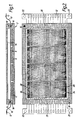
- the semiconductor chip package 2 comprises a row of four RAM chips 4.
- the underside of each chip 4 is adhered to a thermally conductive sheet 6 which constitutes the base of the package 2.
- the base 6 is composed of metal.
- a thin printed circuit 8 overlies the four RAM chips 4.
- the term "printed circuit” is intended to mean a plurality of electroconductive tracks carried on an insulating material.
- the printed circuit 8 is flexible and comprises an electroconductive layer of circuitry, e.g. an array of copper tracks 20, sandwiched between two layers of insulating material, e.g. of polyimide or epoxy.
- outer leads 12 for connection to a printed circuit board (not shown) on which the package is to be mounted, the outer leads 12 being formed by exposure of the electroconductive tracks 20 in the flexible printed circuit 8.
- a lid 14 overlies the flexible printed circuit 8 and has the same dimensions as the base 6.
- the base 6 and lid 14 have peripheral flanges which are provided with complementary registration pegs and holes 16, 18 which enable the base and lid 6, 14 accurately to be located in registry with each other thereby to form a sealed package 2.
- the base 6 and lid 14 are adhered together e.g. by a silicone adhesive along their peripheral mating surfaces so as to seal the package.
- the inner volume of the package 2 may include a material (not shown) which covers the electrical connections in the package and provides protection from moisture penetration of the chips.
- a material may be, for example a conventional moulding material, a "glob top” epoxy as used in known hybrid packages or a self-healing gel contained by a non-hermetic enclosure.
- FIGs 2 to 4 illustrate how the chips 4 are electrically connected to the flexible printed circuit 8.
- the flexible printed circuit 8 comprises an array of electroconductive tracks 20, each of which extends transverse to one or more of the chips 4 and in a direction extending between the opposed outer leads 12.
- Each track 20 is connected, depending upon its function, either to a single respective outer lead 12 at a respective end of the package 2 or to a pair of opposed respective outer leads 12 at respective ends of the package 2.
- the tracks 20 are parallel in that portion of the flexible circuit 8 which overlies the row of chips 4 and the tracks 20 diverge at the opposed ends of the flexible circuit 8 so as to be able to connect to a respective outer lead 12.
- a row of sixteen outer leads 12 is provided at each end 10 of the flexible printed circuit 8.
- a row of twenty outer leads is provided at each end of the printed circuit.
- Each end 10 of the flexible printed circuit 8 is also provided with registration holes 22 to enable the outer leads 12 accurately to be registered onto respective contacts on a printed circuit board (not shown).
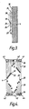
- the flexible circuit 8 as described above, comprises the electroconductive tracks 20 which are sandwiched between a lower insulating layer 24 which is between the tracks 20 and the chips 4 and an upper insulating layer 26 which covers the tracks 20.
- the upper insulating layer 26 is provided with a number of openings 28 each of which exposes a respective bonding pad 30.
- the ends 32, 34 of each chip 4 are each provided, in known manner, with a row of chip bonding pads 36.
- Each chip bonding pad 36 is connected to a respective bonding pad 30 on the flexible circuit by a wire 38 which is bonded at its opposed ends to the two bonding pads 36, 30.
- the bond wires 38 comprise a second level of interconnect which is located above the first level of interconnect constituted by the flexible printed circuit. It will be seen that the interconnections are such that no bond wire 38 overlies any other bond wire 38 so as to avoid any short circuit from being made.
- the tracks 20 are covered by the upper insulating layer 26 of the flexible printed circuit 8, there is no possibility of any bond wire 38 short circuiting by inadvertent contact with a track 20.
- the width of the flexible printed circuit 8 is greater than the length of each chip 4, in order to provide sufficient mechanical strength for the flexible printed circuit.
- three partially-overlapping rectangular holes 40, 42, 44 are cut in the insulating layers 24, 26 of the flexible circuit 8 at a location overlying each row of chip bonding pads 36.
- This enables the bond wires 38 to extend upwardly through the holes 40, 42, 44 from the chip bonding pads 36 thereby to extend over the upper surface of the flexible printed circuit 8 and connect with the respective bonding pads 30.
- there may be provided a group of spaced holes or slots overlying the chip bonding pads. This gives a mechanically more stable flexible printed circuit.
- spaced holes are required when the invention is employed to package an integrated circuit having chip bonding pads on all four of its sides.
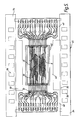
- Figure 5 shows schematically the layout of a portion of an elongate strip 45 including the thin flexible printed circuit 8 prior to connection to the chips 4. For clarity of illustration, any holes which are cut in the thin printed circuit are not shown. However, the printed circuit may be provided with registration holes to allow registration of the thin printed circuit relative to the base of the package.
- the strip consists of a central region 46 comprising the tracks 20 and the bonding pads 30.
- the strip 45 also includes the outer leads 12 at opposed ends of the central region 46. Connected to the outer leads 12 at opposed ends of the portion of the strip 45 are opposed regions of test circuitry 48 which are employed, when the flexible printed circuit 8 has been connected to the chips 4 by the bond wires 38, to test the operation of the packaged semiconductor device.
- the central region 46 also includes opposed, longitudinally directed regions 50 of copper which act mechanically to support the central region 46.
- the central and test regions 46, 48 are bounded on opposed transverse sides by lateral supporting regions 54 which are provided with rows of tractor feed holes 56 which enable the flexible printed circuit 8 to be fed along a production line in a continuous manufacturing process.
- lateral supporting regions 54 which are provided with rows of tractor feed holes 56 which enable the flexible printed circuit 8 to be fed along a production line in a continuous manufacturing process.
- tractor feed holes 56 which enable the flexible printed circuit 8 to be fed along a production line in a continuous manufacturing process.
- the test regions 48 and the lateral supporting regions 54 of the strip are removed so that the final flexible printed circuit 8 is as shown in Figure 2.
- FIGS 6 to 8 illustrate a semiconductor chip package in accordance with a second embodiment of the present invention.
- a semiconductor package 70 consists of a base 72 e.g. of metal to which is adhered a row of semiconductor chips 74. In the illustrated embodiment, there is a row of four RAM chips 74.
- a flexible printed circuit 76 overlies the row of chips 74.
- the flexible printed circuit 76 is carried by a rectangular supporting member 78 which, in the package 70, constitutes a peripheral side wall of the package 70.
- a lid 80 overlies the side wall 78 and the base 72. The base 72 and the lid 80 are sealingly adhered to the side wall 78 thereby to seal the chips 74 inside the package 70.
- a material (not shown) for protecting the chips from moisture may be incorporated in the package 70.
- the thin flexible printed circuit 76 extends outwardly away from opposing longitudinal ends of the package 70 and is provided at opposing ends 82 thereof with a row of upwardly directed outer leads 84.
- the ends 82 of flexible printed circuit 76 are also provided with registration holes 86 to enable the package 70 to be accurately mounted on a printed circuit board (not shown).
- the flexible printed circuit 76 has a different construction from that of the first embodiment and also a different means is employed to connect electrically the chip bonding pads to the flexible printed circuit 76.
- the flexible printed circuit 76 employs a multi-layer tape.
- the flexible printed circuit 76 comprises a lower insulating layer 88 which is disposed against the upper surface 90 of the chips 74.
- a parallel array of electroconductive tracks 92 e.g. of copper is disposed on the lower insulating layer 88.
- the tracks 92 are similar to the tracks 20 of the first embodiment and are connected to respective outer leads 84 at the ends 82 of the flexible printed circuit 76.
- An upper insulating layer 94 covers the tracks 92.
- each track 92 is provided with an upstanding via 96 which extends through the upper insulating layer 94.
- Each via 96 is connected to a respective chip bonding pad 98 by a tape-automated-bonding (TAB) inner lead 100 which extends from the respective via 96 over the upper insulating layer 94 and the TAB inner lead 100 is bonded to the chip bonding pad 98.
- TAB tape-automated-bonding
- the insulated layers 88, 94 of the flexible printed circuit 76 are provided with holes in registry with the chip bonding pads 98, the holes being similar to the holes 40, 42, 44 provided in the first embodiment.
- Figure 7 shows schematically the connections made between the tracks 92 and the chip bonding pads 98 although it will of course be understood that the TAB inner leads do not require the thin wire-like connectors shown schematically in Figure 7 but rather they consist of narrow strips so as to have sufficient mechanical strength at the ends thereof which are to be bonded to the chip bond pads 98.
- the insulating material 88, 94 of the flexible printed circuit 76 extends fully across the width of the package so as to provide increased mechanical strength for the flexible printed circuit 76.
- FIG. 9 is similar to Figure 8 in showing a schematic side view of a chip 110 carrying thereon a flexible printed circuit 112 having electroconductive tracks 114 which are electrically connected to chip bonding pads 116.
- the flexible printed circuit 112 is mounted in the package in the same manner as shown in Figure 6.
- the flexible printed circuit 112 has bonding pads and registration holes (not shown) at respective ends of the flexible printed circuit 112 in a manner similar to those of the second embodiment shown in Figure 7.
- the flexible printed circuit 112 consists of a lower insulating layer 118 which is disposed against the upper surface of the chip 110.
- An upper insulating layer 122 extends over the lower insulating layer 118 and carries in its upper surface a series of longitudinal extending parallel tracks 114 of electroconductive material such as copper. At selected locations on the tracks 114, a via 124 is provided which extends downwardly through the upper insulating layer 122. The via 124 is connected to an end of a transversely-directed electroconductive connector 126 which extends as far as a respective longitudinal edge of the flexible printed circuit 112. The free end 128 of the connector 126 has provided thereon a solder bump 130 which is soldered to a respective chip bonding pad 116.
- the upper insulating layer 122 transversely overlaps the lower insulating layer 118 so as to provide a mechanical support for the end 128 of the connector 126 and the solder bump 130 above the respective chip bonding pad 116.
- the arrangement shown in Figure 9 is designated a "flip-chip" arrangement.
- the flexible printed circuit may be provided with additional electroconductive and insulating layers thereby to provide a plane for power and ground which extends over the row of chips.
- the ground plane acts both to shield the RAMs from any noise generated by the signals across the thin printed circuit and to provide a low inductance path for the logic reference and supply voltages.
- the ground plane outline of the flexible printed circuit is indicated by reference numeral 140.
- the bond wires may be arranged so as to allow decoupling capacitors within the package as disclosed in US Patent No. 4744008.
- the underside of each of the chips is adhered to a thermally conductive sheet constituting the base of the package.
- the sheet spreads the heat out between the chips so that all the chips are within a few degrees of the same temperature.
- the sheet also provides and exceptionally short thermal path to the external surface of the package.
- Particular preferred materials for the thermally conductive sheet are metals which also give excellent mechanical strength, thereby providing a mechanically sound package which is thinner than would be possible using standard package plastics.
- the base of the package may be made of aluminium having a thickness of around 0.038 cm. The thermally conductive sheet constituting the base is actually treated as the top of the package when the package is assembled onto a printed circuit board.
- the outer leads on the flexible printed circuit are connected to a printed circuit board and this results in the base of the package, to which the chips are adhered, being located on the side of the package which is remote from the printed circuit board.
- This further exploits the short thermal path from the chips to the external surface of the package since that surface is directly in contact with air and is able to irradiate heat to adjacent cooler surfaces. Radiation may be assisted, as is conventional with heat sinks, by black anodizing or painting the thermally conductive sheet and by giving the sheet a larger surface area, for example by adding fins to the sheet.
- This orientation of the package also puts the outer leads of the thin printed circuit in the right orientation so that they can be soldered to the printed circuit board without removing the insulating laminate of the thin printed circuit. This keeps the package leads in exact register with respect to each other and overcomes the problems of the fragility of conventional package leads. Furthermore, since a number of chips are assembled in a single package, this means that the package is large enough to dissipate the heat generated by the chips. Normally, the circuitry would be arranged so that only one or two of the chips in the package is or are active at any given time, thus providing that for the one or two active chips, an effective heat sink capability of four chips is available.
- the chips are connected to each other and to external leads by a thin printed circuit which lies over the active circuitry on the chip.
- 96 leads would be required by an assembly of four RAMs consisting of four separate 24 lead packages whereas in the present invention a single package containing four RAMs would require only 32 leads.
- the reduction in the number of leads provides a gain in reliability when compared to the prior art since a reduced number of soldered joints on the board is employed using the multi-clip RAM packages of the present invention.
- mechanical tooling holes are provided adjacent the package leads so that the precise registration of the leads of the package can be extended to register with the printed circuit board without the need for pattern recognition equipment, although this could be employed if appropriate. If the insulating laminate of the thin printed circuit is removed to give unsupported leads, the tooling holes can be put into copper, thereby in effect making wide leads which are particularly appropriate for power and ground terminals.
- the packages of the present invention give great advantage over the prior art constructions in reducing the package size.
- the four RAMs can be closely assembled together in the package and since the flexible printed circuit overlies the RAMs, this greatly reduces the overall size of the package.
- the package consists of four 64K x 4 static RAMs assembled to make 256K x 4 of static RAM in a package having the dimensions 2.64 cm x 1.30 cm x 0.19 cm.
- the smallest standard known package for the 64K x 4 RAM is the so-called SOJ surface mount package which has the dimensions 1.54 cm x 0.86 cm x 0.33 cm, four of which would occupy a printed circuit area (allowing for minimal gaps between components) of 3.18 cm x 1.84 cm.
- the package in accordance with the invention gives an area improvement of about 1.7 times compared to such a known package. This improvement in area is achieved in spite of using a so-called "gull wing" style of lead, (i.e. the leads extend away from the ends of the package and are bent down towards the level of the PCB and are not folded back beneath the package).
- the "gull wing" style of lead employed in the present invention gives a solder joint which is much more easily inspected than the SOJ package.
- the reduction in height achieved by the present invention is also an improvement of about 1.7 times over the prior art, thereby giving a volumetric improvement of the package of the present invention when compared to the prior art of about three times. More significant is a reduction in height to below the 0.254 cm height of conventional solder joints on the solder side of the printed circuit board, allowing the packages of the present invention to be assembled onto the solder side of almost any printed circuit board.
- a further benefit from the height reduction is that a memory board 0.127 cm thick, with the RAM packages of the present invention on both sides, becomes just 0.508 cm thick, which is the height of standard dual-in line packages (DIP's).
- the second illustrated embodiment employs flexible circuit tape such as is used for tape automated bonding (TAB).
- TAB tape automated bonding
- the package in accordance with the present invention can make more effective use of the area of the flexible circuit tape than in the TAB process of the prior art since the TAB tape overlies the chips. If the TAB tape is used in accordance with the present invention, the packages can be made by a continuous flow assembly, employing static burn-in and testing, with consequential benefits in reduced costs of the finished products. This is discussed further below.
- the packages of the present invention can be employed to package any type of integrated circuit either singly or multiply wherein a number of integrated circuits are packaged in a single package.
- the three illustrated embodiments respectively employ bonding wires, tape-automated-bonding (TAB) tape and flip-chip connectors and solder blobs to form a second level of interconnect which is separated from the first level of interconnect, constituted by the tracks of the printed circuit on an insulating layer, by an insulating layer.
- TAB tape-automated-bonding
- solder blobs solder blobs to form a second level of interconnect which is separated from the first level of interconnect, constituted by the tracks of the printed circuit on an insulating layer, by an insulating layer.
- the use of conventional bonding wires reduces the cost of the semiconductor package.
- Such plated through holes if used to connect to tracks acting in place of the bond wires, would need to be on a pitch of about 0.02cm, which, while possible, is not inexpensive.
- the packages of the present invention therefore offer a number of benefits in costs, performance and reliability compared to those of the prior art, both at the level of a single RAM package and at the level of a system which is assembled from single- or multi-chip packages and other components.
- a process for manufacturing multi-chip semiconductor assemblies It is known that in the manufacture of semiconductor chips, statistically only a certain percentage of chips will be fully functional after manufacture. When more than one chip is assembled in a package, the statistical chances of the package containing one or more faulty chips are greatly increased. Accordingly, an effect of using more than one chip in a package is that the yield of fully functional final assemblies may suffer as a result of one of the chips failing before the final test.
- the present invention provides a process for assembling multi-chip packages which not only enables manufacture of fully functional assemblies but also enables manufacture of partly functional assemblies which nevertheless have commercial value.
- FIG 10 shows a process flow in accordance with a further embodiment of the present invention, the process flow relating to the manufacture of microprocessor assemblies which comprise, mounted on a printed circuit board, a single chip microcomputer (e.g. a "Transputer” microcomputer, Transputer being a Registered Trade Mark of INMOS Limited), eight packages of 256K x 4 RAM, the packages being such as those illustrated in Figures 1 to 9, and a semiconductor chip comprising a programmable logic array by means of which the single chip microprocessor accesses the RAMs.
- a single chip microcomputer e.g. a "Transputer” microcomputer, Transputer being a Registered Trade Mark of INMOS Limited
- eight packages of 256K x 4 RAM the packages being such as those illustrated in Figures 1 to 9
- a semiconductor chip comprising a programmable logic array by means of which the single chip microprocessor accesses the RAMs.
- the individual RAM chips are attached to a package base and then the package bases having the required number of chips (e.g. four) attached thereto are assembled in a line on a strip of flexible printed circuit such as that shown in Figure 5.
- the chips are then wire bonded to the flexible printed circuit so as to provide connections such as those shown in Figure 2.
- the package lids are then applied over the package bases and adhered thereto.
- the multi-chip packages may then be tested by making appropriate connections to the test circuitry of the strips and then the strips are subject to a burn-in wherein the strips are heated up so as to induce an infant mortality whereby those chips which would be likely to fail e.g. in the first year of use do so during the burn in process and are thereby discarded and removed from the system.
- the individual packages may then be tested.
- the output from the test is sorted into the N + 1 functional groups, where N is the number of chips assembled in each package.
- One of the groups takes fully functional assemblies i.e. each of the chips in the package is fully functional, N groups take assemblies with a single faulty chip in each of the N possible places for a chip to fail, and the remaining assemblies with more than one faulty chip are discarded.
- each group is singulated into a respective physical bin.
- the printed circuit board assembly is assembled by selecting packages from pre-selected bins and the assembly of the printed circuit board with the components thereon has optional links or programmable decoders which are assembled according to which group or groups are used to build the particular printed circuit board assembly.
- the programmable logic array can have five different programs for the logic depending on which group or groups are selected.
- the printed circuit board assembly may employ packages from a single group which only include packages having the third RAM of the package being faulty. Since the packages used are all identical and are uniformly faulty in a known way, the circuitry or programmable logic array of the printed circuit board can be reliably preselected in response to the known fault of the packages. The assembled printed circuit board would then be finally tested and shipped.
- the present invention thus provides a process flow which permits partly faulty packages conveniently to be employed in the manufacture of a printed circuit board assembly. This can greatly increase the usability of the manufacture of packages and accordingly reduces manufacturing costs.
Landscapes
- Semiconductor Memories (AREA)
- Wire Bonding (AREA)
Applications Claiming Priority (2)
| Application Number | Priority Date | Filing Date | Title |
|---|---|---|---|
| GB8918482 | 1989-08-14 | ||
| GB898918482A GB8918482D0 (en) | 1989-08-14 | 1989-08-14 | Packaging semiconductor chips |
Publications (3)
| Publication Number | Publication Date |
|---|---|
| EP0413451A2 true EP0413451A2 (de) | 1991-02-20 |
| EP0413451A3 EP0413451A3 (en) | 1991-09-04 |
| EP0413451B1 EP0413451B1 (de) | 2002-01-30 |
Family
ID=10661580
Family Applications (1)
| Application Number | Title | Priority Date | Filing Date |
|---|---|---|---|
| EP90308151A Expired - Lifetime EP0413451B1 (de) | 1989-08-14 | 1990-07-25 | Packung von Halbleiterchips |
Country Status (5)
| Country | Link |
|---|---|
| US (2) | US5073816A (de) |
| EP (1) | EP0413451B1 (de) |
| JP (1) | JP3066048B2 (de) |
| DE (1) | DE69033909D1 (de) |
| GB (1) | GB8918482D0 (de) |
Cited By (14)
| Publication number | Priority date | Publication date | Assignee | Title |
|---|---|---|---|---|
| EP0494782A1 (de) * | 1991-01-11 | 1992-07-15 | Texas Instruments Incorporated | Prüf- und Einbrennsystem für einen Wafer und Methode für deren Herstellung |
| EP0501474A3 (en) * | 1991-02-28 | 1993-01-13 | Hitachi, Ltd. | Electronic circuit package |
| EP0551382A4 (en) * | 1990-09-24 | 1993-09-01 | Tessera, Inc. | Semiconductor chip assemblies, methods of making same and components for same |
| US5346861A (en) * | 1990-09-24 | 1994-09-13 | Tessera, Inc. | Semiconductor chip assemblies and methods of making same |
| EP0622840A3 (de) * | 1993-04-07 | 1995-03-22 | Nippon Electric Co | Apparat und Methode für die Montage und das Prüfen von Monolitisch integrierten Mikrowellenschaltungsmodulen (MMIC). |
| GB2289985A (en) * | 1994-05-20 | 1995-12-06 | Matra Marconi Space France | Connecting the output pads on an i.c. chip, using an adaptor board |
| WO1996000981A1 (en) * | 1994-06-29 | 1996-01-11 | Kelsey-Hayes Company | Method and apparatus for manufacturing a programmed electronic control unit for use in an anti-lock braking (abs) system |
| WO1996034408A1 (en) * | 1995-04-26 | 1996-10-31 | Memory Corporation Plc. | Improved test and assembly apparatus |
| US5685885A (en) * | 1990-09-24 | 1997-11-11 | Tessera, Inc. | Wafer-scale techniques for fabrication of semiconductor chip assemblies |
| WO1999044235A1 (en) * | 1998-02-27 | 1999-09-02 | Micron Technology, Inc. | Multichip semiconductor package and method of making |
| US6429028B1 (en) | 2000-08-29 | 2002-08-06 | Dpa Labs, Incorporated | Process to remove semiconductor chips from a plastic package |
| WO2004055895A1 (en) * | 2002-12-12 | 2004-07-01 | Formfactor, Inc. | Integrated circuit assembly |
| US6870276B1 (en) | 2001-12-26 | 2005-03-22 | Micron Technology, Inc. | Apparatus for supporting microelectronic substrates |
| US7098078B2 (en) | 1990-09-24 | 2006-08-29 | Tessera, Inc. | Microelectronic component and assembly having leads with offset portions |
Families Citing this family (25)
| Publication number | Priority date | Publication date | Assignee | Title |
|---|---|---|---|---|
| GB8918482D0 (en) * | 1989-08-14 | 1989-09-20 | Inmos Ltd | Packaging semiconductor chips |
| US5774220A (en) * | 1990-11-20 | 1998-06-30 | Mesacon Gesellschaft Fur Messtechnik Mbh | Continuous contactless measurement of profiles and apparatus for carrying out the measurement process |
| JP2925337B2 (ja) * | 1990-12-27 | 1999-07-28 | 株式会社東芝 | 半導体装置 |
| US5744870A (en) | 1996-06-07 | 1998-04-28 | Micron Technology, Inc. | Memory device with multiple input/output connections |
| US5942798A (en) * | 1997-11-24 | 1999-08-24 | Stmicroelectronics, Inc. | Apparatus and method for automating the underfill of flip-chip devices |
| US5936877A (en) * | 1998-02-13 | 1999-08-10 | Micron Technology, Inc. | Die architecture accommodating high-speed semiconductor devices |
| US6111756A (en) * | 1998-09-11 | 2000-08-29 | Fujitsu Limited | Universal multichip interconnect systems |
| JP3847997B2 (ja) * | 1999-01-22 | 2006-11-22 | 東芝マイクロエレクトロニクス株式会社 | 半導体装置及び両面mcpチップ |
| JP3360723B2 (ja) * | 1999-06-08 | 2002-12-24 | 日本電気株式会社 | 半導体素子のチップサイズパッケージ |
| US6351144B1 (en) * | 1999-07-15 | 2002-02-26 | Altera Corporation | Programmable logic device with unified cell structure including signal interface bumps |
| US6900531B2 (en) * | 2002-10-25 | 2005-05-31 | Freescale Semiconductor, Inc. | Image sensor device |
| US6982566B1 (en) * | 2004-04-01 | 2006-01-03 | Altera Corporation | Method and apparatus for operating a burn-in board to achieve lower equilibrium temperature and to minimize thermal runaway |
| US7701042B2 (en) * | 2006-09-18 | 2010-04-20 | Stats Chippac Ltd. | Integrated circuit package system for chip on lead |
| KR20090021605A (ko) * | 2007-08-27 | 2009-03-04 | 삼성전기주식회사 | 반도체 메모리 패키지 |
| US10177054B2 (en) | 2011-10-27 | 2019-01-08 | Global Circuit Innovations, Inc. | Method for remapping a packaged extracted die |
| US10002846B2 (en) | 2011-10-27 | 2018-06-19 | Global Circuit Innovations Incorporated | Method for remapping a packaged extracted die with 3D printed bond connections |
| US10128161B2 (en) | 2011-10-27 | 2018-11-13 | Global Circuit Innovations, Inc. | 3D printed hermetic package assembly and method |
| US9966319B1 (en) | 2011-10-27 | 2018-05-08 | Global Circuit Innovations Incorporated | Environmental hardening integrated circuit method and apparatus |
| US10147660B2 (en) | 2011-10-27 | 2018-12-04 | Global Circuits Innovations, Inc. | Remapped packaged extracted die with 3D printed bond connections |
| US9870968B2 (en) | 2011-10-27 | 2018-01-16 | Global Circuit Innovations Incorporated | Repackaged integrated circuit and assembly method |
| US9935028B2 (en) * | 2013-03-05 | 2018-04-03 | Global Circuit Innovations Incorporated | Method and apparatus for printing integrated circuit bond connections |
| US10109606B2 (en) | 2011-10-27 | 2018-10-23 | Global Circuit Innovations, Inc. | Remapped packaged extracted die |
| US10115645B1 (en) | 2018-01-09 | 2018-10-30 | Global Circuit Innovations, Inc. | Repackaged reconditioned die method and assembly |
| US11181570B2 (en) | 2018-06-15 | 2021-11-23 | Rosemount Inc. | Partial discharge synthesizer |
| US11508680B2 (en) | 2020-11-13 | 2022-11-22 | Global Circuit Innovations Inc. | Solder ball application for singular die |
Family Cites Families (22)
| Publication number | Priority date | Publication date | Assignee | Title |
|---|---|---|---|---|
| US3780352A (en) * | 1968-06-25 | 1973-12-18 | J Redwanz | Semiconductor interconnecting system using conductive patterns bonded to thin flexible insulating films |
| US3684818A (en) * | 1970-10-20 | 1972-08-15 | Sprague Electric Co | Multi-layer beam-lead wiring for semiconductor packages |
| KR900001273B1 (ko) * | 1983-12-23 | 1990-03-05 | 후지쑤 가부시끼가이샤 | 반도체 집적회로 장치 |
| JPS61111561A (ja) * | 1984-10-05 | 1986-05-29 | Fujitsu Ltd | 半導体装置 |
| CA1238119A (en) * | 1985-04-18 | 1988-06-14 | Douglas W. Phelps, Jr. | Packaged semiconductor chip |
| US4903120A (en) * | 1985-11-22 | 1990-02-20 | Texas Instruments Incorporated | Chip carrier with interconnects on lid |
| US4890152A (en) * | 1986-02-14 | 1989-12-26 | Matsushita Electric Works, Ltd. | Plastic molded chip carrier package and method of fabricating the same |
| US4890153A (en) * | 1986-04-04 | 1989-12-26 | Fairchild Semiconductor Corporation | Single bonding shelf, multi-row wire-bond finger layout for integrated circuit package |
| EP0305398B1 (de) * | 1986-05-01 | 1991-09-25 | Honeywell Inc. | Verbindungsanordnung für mehrere integrierte schaltungen |
| EP0268181B1 (de) * | 1986-11-15 | 1992-07-29 | Matsushita Electric Works, Ltd. | Gegossenes Kunststoff-Chip-Gehäuse mit Steckermuster |
| US4953005A (en) * | 1987-04-17 | 1990-08-28 | Xoc Devices, Inc. | Packaging system for stacking integrated circuits |
| US4914741A (en) * | 1987-06-08 | 1990-04-03 | Digital Equipment Corporation | Tape automated bonding semiconductor package |
| JP2507476B2 (ja) * | 1987-09-28 | 1996-06-12 | 株式会社東芝 | 半導体集積回路装置 |
| JP2706077B2 (ja) * | 1988-02-12 | 1998-01-28 | 株式会社日立製作所 | 樹脂封止型半導体装置及びその製造方法 |
| GB2218847B (en) * | 1988-05-16 | 1991-04-24 | Gen Electric Co Plc | Carrier for semiconductor devices |
| IL90601A0 (en) * | 1988-06-24 | 1990-01-18 | Unistructure Inc | Protected lead frames for inter-connecting semiconductor devices and their fabrication |
| US4939570A (en) * | 1988-07-25 | 1990-07-03 | International Business Machines, Corp. | High power, pluggable tape automated bonding package |
| JPH02174255A (ja) * | 1988-12-27 | 1990-07-05 | Mitsubishi Electric Corp | 半導体集積回路装置 |
| US4912547A (en) * | 1989-01-30 | 1990-03-27 | International Business Machines Corporation | Tape bonded semiconductor device |
| GB8918482D0 (en) * | 1989-08-14 | 1989-09-20 | Inmos Ltd | Packaging semiconductor chips |
| US5045921A (en) * | 1989-12-26 | 1991-09-03 | Motorola, Inc. | Pad array carrier IC device using flexible tape |
| US5018005A (en) * | 1989-12-27 | 1991-05-21 | Motorola Inc. | Thin, molded, surface mount electronic device |
-
1989
- 1989-08-14 GB GB898918482A patent/GB8918482D0/en active Pending
-
1990
- 1990-07-25 DE DE69033909T patent/DE69033909D1/de not_active Expired - Lifetime
- 1990-07-25 EP EP90308151A patent/EP0413451B1/de not_active Expired - Lifetime
- 1990-07-25 US US07/557,940 patent/US5073816A/en not_active Expired - Lifetime
- 1990-08-08 JP JP2210119A patent/JP3066048B2/ja not_active Expired - Lifetime
-
1994
- 1994-10-21 US US08/327,447 patent/US6100581A/en not_active Expired - Lifetime
Cited By (29)
| Publication number | Priority date | Publication date | Assignee | Title |
|---|---|---|---|---|
| US7098078B2 (en) | 1990-09-24 | 2006-08-29 | Tessera, Inc. | Microelectronic component and assembly having leads with offset portions |
| US5685885A (en) * | 1990-09-24 | 1997-11-11 | Tessera, Inc. | Wafer-scale techniques for fabrication of semiconductor chip assemblies |
| EP0551382A4 (en) * | 1990-09-24 | 1993-09-01 | Tessera, Inc. | Semiconductor chip assemblies, methods of making same and components for same |
| US5848467A (en) * | 1990-09-24 | 1998-12-15 | Tessera, Inc. | Methods of making semiconductor chip assemblies |
| US5346861A (en) * | 1990-09-24 | 1994-09-13 | Tessera, Inc. | Semiconductor chip assemblies and methods of making same |
| US5347159A (en) * | 1990-09-24 | 1994-09-13 | Tessera, Inc. | Semiconductor chip assemblies with face-up mounting and rear-surface connection to substrate |
| US5682061A (en) * | 1990-09-24 | 1997-10-28 | Tessera, Inc. | Component for connecting a semiconductor chip to a substrate |
| EP1111672A3 (de) * | 1990-09-24 | 2002-09-18 | Tessera, Inc. | Halbleiterchipanordnungen, Herstellungsmethoden und Komponenten für dieselbe |
| US7271481B2 (en) | 1990-09-24 | 2007-09-18 | Tessera, Inc. | Microelectronic component and assembly having leads with offset portions |
| US5307010A (en) * | 1991-01-11 | 1994-04-26 | Texas Instruments Incorporated | Wafer burn-in and test system |
| US5532614A (en) * | 1991-01-11 | 1996-07-02 | Texas Instruments Incorporated | Wafer burn-in and test system |
| US5444366A (en) * | 1991-01-11 | 1995-08-22 | Texas Instruments Incorporated | Wafer burn-in and test system |
| EP0494782A1 (de) * | 1991-01-11 | 1992-07-15 | Texas Instruments Incorporated | Prüf- und Einbrennsystem für einen Wafer und Methode für deren Herstellung |
| EP0501474A3 (en) * | 1991-02-28 | 1993-01-13 | Hitachi, Ltd. | Electronic circuit package |
| EP0622840A3 (de) * | 1993-04-07 | 1995-03-22 | Nippon Electric Co | Apparat und Methode für die Montage und das Prüfen von Monolitisch integrierten Mikrowellenschaltungsmodulen (MMIC). |
| GB2289985B (en) * | 1994-05-20 | 1998-04-01 | Matra Marconi Space France | Method of connecting the output pads on an integrated circuit chip,and multichip module thus obtained |
| GB2289985A (en) * | 1994-05-20 | 1995-12-06 | Matra Marconi Space France | Connecting the output pads on an i.c. chip, using an adaptor board |
| WO1996000981A1 (en) * | 1994-06-29 | 1996-01-11 | Kelsey-Hayes Company | Method and apparatus for manufacturing a programmed electronic control unit for use in an anti-lock braking (abs) system |
| WO1996034408A1 (en) * | 1995-04-26 | 1996-10-31 | Memory Corporation Plc. | Improved test and assembly apparatus |
| US6228548B1 (en) | 1998-02-27 | 2001-05-08 | Micron Technology, Inc. | Method of making a multichip semiconductor package |
| US6429528B1 (en) | 1998-02-27 | 2002-08-06 | Micron Technology, Inc. | Multichip semiconductor package |
| WO1999044235A1 (en) * | 1998-02-27 | 1999-09-02 | Micron Technology, Inc. | Multichip semiconductor package and method of making |
| US6906409B2 (en) | 1998-02-27 | 2005-06-14 | Micron Technology, Inc. | Multichip semiconductor package |
| US6429028B1 (en) | 2000-08-29 | 2002-08-06 | Dpa Labs, Incorporated | Process to remove semiconductor chips from a plastic package |
| US6870276B1 (en) | 2001-12-26 | 2005-03-22 | Micron Technology, Inc. | Apparatus for supporting microelectronic substrates |
| US6995026B2 (en) | 2001-12-26 | 2006-02-07 | Micron Technology, Inc. | Methods for coupling a flowable conductive material to microelectronic substrates |
| US6936916B2 (en) | 2001-12-26 | 2005-08-30 | Micron Technology, Inc. | Microelectronic assemblies and electronic devices including connection structures with multiple elongated members |
| WO2004055895A1 (en) * | 2002-12-12 | 2004-07-01 | Formfactor, Inc. | Integrated circuit assembly |
| US7550842B2 (en) | 2002-12-12 | 2009-06-23 | Formfactor, Inc. | Integrated circuit assembly |
Also Published As
| Publication number | Publication date |
|---|---|
| DE69033909D1 (de) | 2002-03-14 |
| JP3066048B2 (ja) | 2000-07-17 |
| JPH0382132A (ja) | 1991-04-08 |
| GB8918482D0 (en) | 1989-09-20 |
| US6100581A (en) | 2000-08-08 |
| US5073816A (en) | 1991-12-17 |
| EP0413451A3 (en) | 1991-09-04 |
| EP0413451B1 (de) | 2002-01-30 |
Similar Documents
| Publication | Publication Date | Title |
|---|---|---|
| US5073816A (en) | Packaging semiconductor chips | |
| US5817535A (en) | LOC SIMM and method of fabrication | |
| US6738263B2 (en) | Stackable ball grid array package | |
| US7279797B2 (en) | Module assembly and method for stacked BGA packages | |
| CN1112086C (zh) | 中心密集的周边球栅阵列电路封装和封装方法 | |
| US6110762A (en) | Method of manufacturing a custom corner attach heat sink design for a plastic ball grid array integrated circuit package | |
| US5434750A (en) | Partially-molded, PCB chip carrier package for certain non-square die shapes | |
| US5262927A (en) | Partially-molded, PCB chip carrier package | |
| US5942795A (en) | Leaded substrate carrier for integrated circuit device and leaded substrate carrier device assembly | |
| US5483024A (en) | High density semiconductor package | |
| US20030084566A1 (en) | Chip scale package with heat spreader and method of manufacture | |
| JP3113005B2 (ja) | キャリアのない集積回路パッケージ | |
| US20050248038A1 (en) | Chip scale package with heat spreader | |
| US5866941A (en) | Ultra thin, leadless and molded surface mount integrated circuit package | |
| KR0145641B1 (ko) | 반도체 집적 회로 장치 | |
| US20030080418A1 (en) | Semiconductor device having power supply pads arranged between signal pads and substrate edge | |
| USRE43112E1 (en) | Stackable ball grid array package |
Legal Events
| Date | Code | Title | Description |
|---|---|---|---|
| PUAI | Public reference made under article 153(3) epc to a published international application that has entered the european phase |
Free format text: ORIGINAL CODE: 0009012 |
|
| AK | Designated contracting states |
Kind code of ref document: A2 Designated state(s): DE FR GB IT NL |
|
| PUAL | Search report despatched |
Free format text: ORIGINAL CODE: 0009013 |
|
| AK | Designated contracting states |
Kind code of ref document: A3 Designated state(s): DE FR GB IT NL |
|
| 17P | Request for examination filed |
Effective date: 19911102 |
|
| 17Q | First examination report despatched |
Effective date: 19930528 |
|
| RAP1 | Party data changed (applicant data changed or rights of an application transferred) |
Owner name: SGS-THOMSON MICROELECTRONICS LIMITED |
|
| APAB | Appeal dossier modified |
Free format text: ORIGINAL CODE: EPIDOS NOAPE |
|
| APAD | Appeal reference recorded |
Free format text: ORIGINAL CODE: EPIDOS REFNE |
|
| APAD | Appeal reference recorded |
Free format text: ORIGINAL CODE: EPIDOS REFNE |
|
| RAP3 | Party data changed (applicant data changed or rights of an application transferred) |
Owner name: STMICROELECTRONICS LIMITED |
|
| APCB | Communication from the board of appeal sent |
Free format text: ORIGINAL CODE: EPIDOS OBAPE |
|
| APCB | Communication from the board of appeal sent |
Free format text: ORIGINAL CODE: EPIDOS OBAPE |
|
| APAB | Appeal dossier modified |
Free format text: ORIGINAL CODE: EPIDOS NOAPE |
|
| APBJ | Interlocutory revision of appeal recorded |
Free format text: ORIGINAL CODE: EPIDOS IRAPE |
|
| GRAG | Despatch of communication of intention to grant |
Free format text: ORIGINAL CODE: EPIDOS AGRA |
|
| GRAH | Despatch of communication of intention to grant a patent |
Free format text: ORIGINAL CODE: EPIDOS IGRA |
|
| GRAH | Despatch of communication of intention to grant a patent |
Free format text: ORIGINAL CODE: EPIDOS IGRA |
|
| GRAA | (expected) grant |
Free format text: ORIGINAL CODE: 0009210 |
|
| REG | Reference to a national code |
Ref country code: GB Ref legal event code: IF02 |
|
| AK | Designated contracting states |
Kind code of ref document: B1 Designated state(s): DE FR GB IT NL |
|
| PG25 | Lapsed in a contracting state [announced via postgrant information from national office to epo] |
Ref country code: IT Free format text: LAPSE BECAUSE OF FAILURE TO SUBMIT A TRANSLATION OF THE DESCRIPTION OR TO PAY THE FEE WITHIN THE PRE;WARNING: LAPSES OF ITALIAN PATENTS WITH EFFECTIVE DATE BEFORE 2007 MAY HAVE OCCURRED AT ANY TIME BEFORE 2007. THE CORRECT EFFECTIVE DATE MAY BE DIFFERENT FROM THE ONE RECORDED.SCRIBED TIME-LIMIT Effective date: 20020130 Ref country code: NL Free format text: LAPSE BECAUSE OF FAILURE TO SUBMIT A TRANSLATION OF THE DESCRIPTION OR TO PAY THE FEE WITHIN THE PRESCRIBED TIME-LIMIT Effective date: 20020130 Ref country code: FR Free format text: LAPSE BECAUSE OF FAILURE TO SUBMIT A TRANSLATION OF THE DESCRIPTION OR TO PAY THE FEE WITHIN THE PRESCRIBED TIME-LIMIT Effective date: 20020130 |
|
| REF | Corresponds to: |
Ref document number: 69033909 Country of ref document: DE Date of ref document: 20020314 |
|
| PG25 | Lapsed in a contracting state [announced via postgrant information from national office to epo] |
Ref country code: DE Free format text: LAPSE BECAUSE OF FAILURE TO SUBMIT A TRANSLATION OF THE DESCRIPTION OR TO PAY THE FEE WITHIN THE PRESCRIBED TIME-LIMIT Effective date: 20020501 |
|
| NLV1 | Nl: lapsed or annulled due to failure to fulfill the requirements of art. 29p and 29m of the patents act | ||
| PG25 | Lapsed in a contracting state [announced via postgrant information from national office to epo] |
Ref country code: GB Free format text: LAPSE BECAUSE OF NON-PAYMENT OF DUE FEES Effective date: 20020725 |
|
| EN | Fr: translation not filed | ||
| PLBE | No opposition filed within time limit |
Free format text: ORIGINAL CODE: 0009261 |
|
| STAA | Information on the status of an ep patent application or granted ep patent |
Free format text: STATUS: NO OPPOSITION FILED WITHIN TIME LIMIT |
|
| 26N | No opposition filed | ||
| GBPC | Gb: european patent ceased through non-payment of renewal fee |
Effective date: 20020725 |
|
| APAH | Appeal reference modified |
Free format text: ORIGINAL CODE: EPIDOSCREFNO |