EP0411933A2 - Dispositif d'affichage à matrice active - Google Patents
Dispositif d'affichage à matrice active Download PDFInfo
- Publication number
- EP0411933A2 EP0411933A2 EP90308491A EP90308491A EP0411933A2 EP 0411933 A2 EP0411933 A2 EP 0411933A2 EP 90308491 A EP90308491 A EP 90308491A EP 90308491 A EP90308491 A EP 90308491A EP 0411933 A2 EP0411933 A2 EP 0411933A2
- Authority
- EP
- European Patent Office
- Prior art keywords
- line
- storage capacity
- lines
- common main
- display apparatus
- Prior art date
- Legal status (The legal status is an assumption and is not a legal conclusion. Google has not performed a legal analysis and makes no representation as to the accuracy of the status listed.)
- Granted
Links
Images


Classifications
-
- G—PHYSICS
- G09—EDUCATION; CRYPTOGRAPHY; DISPLAY; ADVERTISING; SEALS
- G09G—ARRANGEMENTS OR CIRCUITS FOR CONTROL OF INDICATING DEVICES USING STATIC MEANS TO PRESENT VARIABLE INFORMATION
- G09G3/00—Control arrangements or circuits, of interest only in connection with visual indicators other than cathode-ray tubes
- G09G3/20—Control arrangements or circuits, of interest only in connection with visual indicators other than cathode-ray tubes for presentation of an assembly of a number of characters, e.g. a page, by composing the assembly by combination of individual elements arranged in a matrix no fixed position being assigned to or needed to be assigned to the individual characters or partial characters
- G09G3/34—Control arrangements or circuits, of interest only in connection with visual indicators other than cathode-ray tubes for presentation of an assembly of a number of characters, e.g. a page, by composing the assembly by combination of individual elements arranged in a matrix no fixed position being assigned to or needed to be assigned to the individual characters or partial characters by control of light from an independent source
- G09G3/36—Control arrangements or circuits, of interest only in connection with visual indicators other than cathode-ray tubes for presentation of an assembly of a number of characters, e.g. a page, by composing the assembly by combination of individual elements arranged in a matrix no fixed position being assigned to or needed to be assigned to the individual characters or partial characters by control of light from an independent source using liquid crystals
- G09G3/3611—Control of matrices with row and column drivers
- G09G3/3648—Control of matrices with row and column drivers using an active matrix
- G09G3/3655—Details of drivers for counter electrodes, e.g. common electrodes for pixel capacitors or supplementary storage capacitors
-
- G—PHYSICS
- G09—EDUCATION; CRYPTOGRAPHY; DISPLAY; ADVERTISING; SEALS
- G09G—ARRANGEMENTS OR CIRCUITS FOR CONTROL OF INDICATING DEVICES USING STATIC MEANS TO PRESENT VARIABLE INFORMATION
- G09G2320/00—Control of display operating conditions
- G09G2320/02—Improving the quality of display appearance
- G09G2320/0223—Compensation for problems related to R-C delay and attenuation in electrodes of matrix panels, e.g. in gate electrodes or on-substrate video signal electrodes
Definitions
- This invention relates to an active matrix display apparatus having a storage capacity.
- An active matrix system of the type having pixel electrodes arranged in a matrix fashion on an insulating substrate so that the pixel.electrodes are independently driven has been employed in display apparatuses using liquid crystals.
- Such an active matrix system has often been employed especially in large-sized display apparatuses geared for high-density display.
- TFT Thin film transistor
- MOS transistor devices MOS transistor devices
- HIM metal - insulator - metal
- diodes diodes
- varistors varistors, and the like
- An active matrix drive system affords high contrast display and indeed it has been put into practical use in various areas of application, including liquid crystal television, word processors, and terminal display units for computers.
- FIG. 4 shows a plan view of a conventional active matrix display apparatus, which includes an active matrix board 1 and a counter substrate 2 placed upon the board 1.
- TFTs are used as switching devices.
- a display medium such as a liquid crystal, is contained in the space between the active matrix board 1 and the counter substrate 2 to thereby form the display apparatus.
- FIG 5 schematically illustrates the active matrix board 1 shown in Figure 4.
- the active matrix board 1 comprises gate bus lines 7, source bus lines 9, intersecting the gate bus lines 7, and storage capacity lines (i.e., addition capacity lines) 8 arranged in a parallel relation to the gate bus lines 7. All the storage capacity lines 8 are connected to a common main line 6 for storage capacities.
- FIG. 2 is a schematic diagram showing a rectangular area surrounded by source bus lines 9, a gate bus line 7 and a storage capacity line 8 as are shown in Figure 5.
- a gate electrode 21 of a TFT 10 is connected to the gate bus line 7, and a gate electrode 22 of the TFT 10 is connected to one of the source bus lines 9.
- a drain electrode 23 is connected to a pixel electrode 11.
- a storage capacity 12 is formed between a storage capacity electrode (i.e., an addition capacity electrode) 24 connected to the storage capacity line 8 and the pixel electrode 11.
- Each gate bus line 7, each source bus line 9, and each storage capacity line 8 are made of metal or other conductive materials and respectively have electric resistances R (G), R (S), and R (Cs). These lines 7, 9 and 8 respectively have capacities C (G), C (S), and C (Cs) formed between the individual lines 7, 9 and 8 as one part and other individual intersecting lines and counter electrodes as the other part. Therefore, on the respective lines 7, 9 and 8 there will occur signal delays corresponding to time constants ⁇ (G), ⁇ (S), ⁇ (Cs) represented by products of the respective resistances and the respective capacities. Because of such signal delay, a signal applied to the terminal of each respective line will delay as it advances toward the leading end of the line.
- ⁇ (G) and ⁇ (S) on the gate bus line 7 and source bus line 9 respectively, where a signal delay on the storage capacity line 8 depends on the value of ⁇ (Cs) plus ⁇ (Cs 0) on the common main line 6. Since all storage capacity lines 8 are connected to the common main line 6, the value of ⁇ (Cs 0) is an enormous one. Therefore, a signal applied to common line terminals 5a and 5b will delay on the common main line 6 and further delay on the storage capacity line 8.
- a signal delay on the common main line 6 is greatest at a central part of the line 6 which is remotest from the common line terminals 5a and 5b.
- a signal delay on the storage capacity line 8 is largest at a portion of the line 8 which is remotest from the common main line 6.
- a signal delay is largest at a central portion of the board at the right end thereof.
- a trial calculation can be made with respect to a liquid crystal display apparatus having a diagonal of the order of 14 inches.
- the material of the common main line 6 is Ti metal (with a specific resistance of 10 ⁇ 4 ⁇ cm) and that the line 6 is 4000 ⁇ in thickness, 2 mm in width, and 200 mm in length
- the resistance over the entire length of the common main line 6 is about 250 ⁇ .
- the capacity of the common main line 6 is more than 0.2 ⁇ F
- the time constant at the center portion of the common main line 6 at which the signal delay is greatest is more than 12.5 ⁇ sec.
- the required write time for a data signal is about 30 ⁇ sec. It can be understood from this that the above-mentioned time constant value is unacceptably large. Therefore, the display apparatus is subject to considerable display irregularities.
- the active matrix display apparatus of this invention which overcomes the above-discussed and numerous other disadvantages and deficiencies of the prior art, comprises an active matrix display apparatus comprising pixel electrodes arranged in a matrix fashion on an insulating substrate, storage capacity electrodes arranged opposite to said pixel electrodes, storage capacity lines connected individually to said storage capacity electrodes, a common main line connected to said storage capacity lines, at least one branch line branched from said common main line, and a branch terminal formed at the leading end of said branch line.
- the common main line is connected to one end of said storage capacity line.
- the common main lines are connected to respective opposite ends of said storage capacity lines.
- the invention described herein makes possible the objectives of (1) providing an active matrix display apparatus having storage capacity lines which are less likely to involve a signal delay; and (2) providing an active matrix display apparatus that has a branch line branched from a common main line, and a branch terminal formed at the leading end of the branch line, and according a signal delay if any, can be minimized on the storage capacity lines, whereby the display apparatus of the invention provides a higher level of image quality and is capable of meeting the requirements for larger size construction and a higher degree of sophistication for such a display apparatus.
- the active matrix display apparatus of this invention has, in addition to common line terminals at both ends of a common main line, a branch terminal provided at the leading end of a branch line branched from the common main line.
- the branch terminal functions as a signal input in the same manner as the common line terminals, and accordingly the common main line is divided at the point at which the branch line is branched from the common main line. Therefore, the respective divisional portions of the common main line are reduced in resistance and capacity and thus the problem of signal delay can be effectively solved.
- one branch line is provided at a median point of the common main line and a branch terminal is provided at the leading end of the branch line, whereby the common main line is equally divided into two parts. Accordingly, the resistance and capacity of the common main line are halved between the respective half portions of the common main line so divided. Therefore, the time constant which represents a signal delay on the common main line is reduced to one quarter thereof.
- the time constant on the common main line is reduced to one ninth.
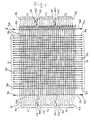
- FIG 1 is a schematic diagram showing one example of an active matrix board 1 employed in the display apparatus according to the invention.
- a fragmentary enlarged view of the board in Figure 1 is such as that shown in Figure 2.
- the active matrix display apparatus in this example comprises pixel electrodes 11 arranged in a matrix fashion on an insulating substrate, storage capacity electrodes 24 arranged opposite to the pixel electrodes 11, storage capacity lines 8 connected to the storage capacity electrodes 24, a common main line 6 connected to the storage capacity lines 8 at one end thereof, a branch line 17 branched from the common main line 6, and a branch terminal 16 formed at the leading end of the branch line 17.
- Gate bus lines 7 parallel to each other are arranged between the individual pixel electrodes 11, and source bus lines 9 are arranged in an intersecting relation with the gate bus lines 7.
- the gate bus lines 7 are parallel to the storage capacity lines 8.
- a gate electrode 21 of a TFT 10 is connected to one gate bus line 7, and a source electrode 22 of the TFT 10 is connected to one source bus line 9.
- a drain electrode 23 of the TFT 10 is connected to one pixel electrode 11.
- a storage capacity 12 is formed between the storage capacity electrode 24 connected to the storage capacity line 8 and the pixel electrode 11.
- source bus lines 9 each having a source signal terminal 3a on one side of the substrate 1 and source bus lines 9 each having a source signal terminal 3b on the other side of the substrate 1, are arranged in an alternate relation.
- a gate signal terminal 4 is provided at one end of each gate bus line 7.
- the common main line 6 is provided on that side of the substrate 1 which is opposite to the side on which each gate signal terminal 4 is provided.
- the common main line 6 is connected to all the storage capacity lines 8.
- Common line terminals 5a and 5b are provided respectively at opposite ends of the common main line 6.
- the branch line 17 is branched from a median-point of the common main line 6.
- the branch terminal 16 is provided at the leading end of the branch line 17.
- the common line terminals 5a, 5b and the branch terminal 16 are used as signal inputs and, therefore, the common main line 6 is divided into two equal parts at the point at which the branch line 17 is branched from the common main line 6.
- the resistance and capacity of two equal half portions each of the common main line 6 correspond to one half values of those of a common main line having no such a branch line 17.
- the time constant on the common main line 6 is one fourth of that on a common main line having no branch line, a possible signal delay being thus considerably reduced.
- FIG. 3 Another example of the active matrix board employed in the display apparatus of this invention is shown in Figure 3.
- the gate bus lines 7 are divided into three blocks of gate bus lines 7a, 7b, 7c.
- the individual gate bus lines 7a, 7b, 7c each have gate signal terminals 4a and 4b provided at both ends thereof.
- scan signals are applied from both ends of the individual gate bus lines 7a, 7b, 7c and data signals are applied from both ends of the individual source bus lines 9.
- the storage capacity lines 8 are also divided into three blocks of storage capacity lines 8a, 8b, 8c.
- Common main lines 6a and 6b are connected respectively to opposite ends of each storage capacity line 8. In this example, therefore, signals are input from both ends of each storage capacity line 8.
- common line terminals 5a and 5b and 5c and 5d At both ends of the common main lines 6a and 6b there are provided common line terminals 5a and 5b and 5c and 5d.
- Branch lines 17a and 17b, and 17c and 17d are provided at points at which the respective common main lines 6a and 6b are divided into three equal parts. At ends of the respective branch lines 17a, 17b, 17c, 17d are provided branch terminals 16a, 16b, 16c, 16d.
- the common line terminals 5a, 5b, 5c, 5d and the branch terminals 16a, 16b, 16c, 16d are all used as signal inputs.
- the time constant on the common main line 6a is one ninth of that on a common main line having no branch line 17a, 17b.
- the time constant on the common main line 6b is one ninth of that on a common main line having no branch line 17c, 17d.
Landscapes
- Engineering & Computer Science (AREA)
- Power Engineering (AREA)
- Chemical & Material Sciences (AREA)
- Crystallography & Structural Chemistry (AREA)
- Physics & Mathematics (AREA)
- Computer Hardware Design (AREA)
- General Physics & Mathematics (AREA)
- Theoretical Computer Science (AREA)
- Liquid Crystal (AREA)
- Devices For Indicating Variable Information By Combining Individual Elements (AREA)
- Liquid Crystal Display Device Control (AREA)
Applications Claiming Priority (2)
| Application Number | Priority Date | Filing Date | Title |
|---|---|---|---|
| JP201973/89 | 1989-08-03 | ||
| JP1201973A JPH0364735A (ja) | 1989-08-03 | 1989-08-03 | アクティブマトリクス表示装置 |
Publications (3)
| Publication Number | Publication Date |
|---|---|
| EP0411933A2 true EP0411933A2 (fr) | 1991-02-06 |
| EP0411933A3 EP0411933A3 (en) | 1992-06-03 |
| EP0411933B1 EP0411933B1 (fr) | 1994-10-26 |
Family
ID=16449832
Family Applications (1)
| Application Number | Title | Priority Date | Filing Date |
|---|---|---|---|
| EP90308491A Expired - Lifetime EP0411933B1 (fr) | 1989-08-03 | 1990-08-01 | Dispositif d'affichage à matrice active |
Country Status (4)
| Country | Link |
|---|---|
| US (1) | US5446568A (fr) |
| EP (1) | EP0411933B1 (fr) |
| JP (1) | JPH0364735A (fr) |
| DE (1) | DE69013610T2 (fr) |
Families Citing this family (8)
| Publication number | Priority date | Publication date | Assignee | Title |
|---|---|---|---|---|
| US5422293A (en) * | 1991-12-24 | 1995-06-06 | Casio Computer Co., Ltd. | Method for manufacturing a TFT panel |
| US5822026A (en) * | 1994-02-17 | 1998-10-13 | Seiko Epson Corporation | Active matrix substrate and color liquid crystal display |
| KR0139319B1 (ko) * | 1994-11-14 | 1998-06-15 | 김광호 | 한 화소에 이중배선과 복수의 트랜지스터를 구비한 액정 표시 장치 |
| JP4070896B2 (ja) * | 1998-10-07 | 2008-04-02 | 三菱電機株式会社 | 電気光学素子および該電気光学素子の製造方法 |
| TW594156B (en) | 2002-01-04 | 2004-06-21 | Fujitsu Display Tech | Substrate for display device and display device equipped therewith |
| KR101017192B1 (ko) * | 2004-06-28 | 2011-02-25 | 엘지디스플레이 주식회사 | 액정표시장치 |
| JP2015118205A (ja) | 2013-12-18 | 2015-06-25 | パナソニック液晶ディスプレイ株式会社 | 液晶表示装置 |
| JP2015121729A (ja) | 2013-12-25 | 2015-07-02 | パナソニック液晶ディスプレイ株式会社 | 液晶表示装置 |
Citations (2)
| Publication number | Priority date | Publication date | Assignee | Title |
|---|---|---|---|---|
| GB2173628A (en) * | 1985-03-15 | 1986-10-15 | Sharp Kk | Liquid crystal display devices |
| EP0216188A2 (fr) * | 1985-08-29 | 1987-04-01 | Canon Kabushiki Kaisha | Panneau d'affichage matriciel |
Family Cites Families (7)
| Publication number | Priority date | Publication date | Assignee | Title |
|---|---|---|---|---|
| JPS5844743A (ja) * | 1981-09-10 | 1983-03-15 | Fujitsu Ltd | 半導体集積回路 |
| EP0348017B1 (fr) * | 1982-06-30 | 1993-12-15 | Fujitsu Limited | Dispositif de circuit intégré semi-conducteur |
| JPS60101951A (ja) * | 1983-11-08 | 1985-06-06 | Sanyo Electric Co Ltd | ゲ−トアレイ |
| JPS62265688A (ja) * | 1986-05-13 | 1987-11-18 | 松下電器産業株式会社 | アクテイブマトリツクスアレイ |
| JPS6344742A (ja) * | 1986-08-12 | 1988-02-25 | Fujitsu Ltd | 半導体装置 |
| US4906072A (en) * | 1986-10-09 | 1990-03-06 | Canon Kabushiki Kaisha | Display apparatus and driving method for providing an uniform potential to the electrodes |
| US5076667A (en) * | 1990-01-29 | 1991-12-31 | David Sarnoff Research Center, Inc. | High speed signal and power supply bussing for liquid crystal displays |
-
1989
- 1989-08-03 JP JP1201973A patent/JPH0364735A/ja active Pending
-
1990
- 1990-08-01 EP EP90308491A patent/EP0411933B1/fr not_active Expired - Lifetime
- 1990-08-01 DE DE69013610T patent/DE69013610T2/de not_active Expired - Fee Related
-
1992
- 1992-07-06 US US07/908,749 patent/US5446568A/en not_active Expired - Lifetime
Patent Citations (2)
| Publication number | Priority date | Publication date | Assignee | Title |
|---|---|---|---|---|
| GB2173628A (en) * | 1985-03-15 | 1986-10-15 | Sharp Kk | Liquid crystal display devices |
| EP0216188A2 (fr) * | 1985-08-29 | 1987-04-01 | Canon Kabushiki Kaisha | Panneau d'affichage matriciel |
Also Published As
| Publication number | Publication date |
|---|---|
| DE69013610D1 (de) | 1994-12-01 |
| US5446568A (en) | 1995-08-29 |
| EP0411933A3 (en) | 1992-06-03 |
| DE69013610T2 (de) | 1995-05-04 |
| EP0411933B1 (fr) | 1994-10-26 |
| JPH0364735A (ja) | 1991-03-20 |
Similar Documents
| Publication | Publication Date | Title |
|---|---|---|
| US4840460A (en) | Apparatus and method for providing a gray scale capability in a liquid crystal display unit | |
| US5946068A (en) | Liquid crystal display with dummy data driving to produce edge column compensation | |
| JPH052969B2 (fr) | ||
| US6483495B2 (en) | Liquid crystal display device | |
| US5745090A (en) | Wiring structure and driving method for storage capacitors in a thin film transistor liquid crystal display device | |
| EP1506450A1 (fr) | Dispositif a affichage a cristaux liquides bistables comprenant des electrodes d'images a structure a peigne | |
| EP0411933B1 (fr) | Dispositif d'affichage à matrice active | |
| JPH06281959A (ja) | アクティブマトリックス液晶表示装置 | |
| WO2004046793A2 (fr) | Afficheur a cristaux liquides et son procede de commande | |
| JP3069280B2 (ja) | アクティブマトリックス型液晶表示素子及びその駆動方法 | |
| JP4480821B2 (ja) | 液晶表示装置 | |
| US6396555B1 (en) | LCD panel in which the scanning line and the line connected to the drain of the TFT are parallel | |
| US5373378A (en) | Active matrix type liquid crystal display device with peripheral pixel electrodes attached directly to signal lines | |
| KR19990068160A (ko) | 평면표시장치 및 그 표시방법 | |
| JP3656179B2 (ja) | アクティブマトリックス型液晶表示素子及びその駆動方法 | |
| JP3064702B2 (ja) | アクティブマトリクス型液晶表示装置 | |
| KR20030080324A (ko) | 라인 온 글래스형 액정표시장치 | |
| JPH02223913A (ja) | アクテイブマトリクス液晶デイスプレイ | |
| JPH09258261A (ja) | 液晶パネル | |
| JPH05224239A (ja) | アクティブマトリクス液晶表示ディスプレイ | |
| JPH08179371A (ja) | 薄膜トランジスタ液晶表示装置およびその駆動法 | |
| CN109791754A (zh) | 显示面板 | |
| KR100855486B1 (ko) | 라인 온 글래스형 액정표시장치 | |
| KR100431627B1 (ko) | 액정표시장치및그구동방법 | |
| KR100188114B1 (ko) | 박막 트랜지스터 액정 표시 장치 |
Legal Events
| Date | Code | Title | Description |
|---|---|---|---|
| PUAI | Public reference made under article 153(3) epc to a published international application that has entered the european phase |
Free format text: ORIGINAL CODE: 0009012 |
|
| AK | Designated contracting states |
Kind code of ref document: A2 Designated state(s): DE FR GB NL |
|
| 17P | Request for examination filed |
Effective date: 19901228 |
|
| PUAL | Search report despatched |
Free format text: ORIGINAL CODE: 0009013 |
|
| AK | Designated contracting states |
Kind code of ref document: A3 Designated state(s): DE FR GB NL |
|
| 17Q | First examination report despatched |
Effective date: 19931122 |
|
| GRAA | (expected) grant |
Free format text: ORIGINAL CODE: 0009210 |
|
| AK | Designated contracting states |
Kind code of ref document: B1 Designated state(s): DE FR GB NL |
|
| REF | Corresponds to: |
Ref document number: 69013610 Country of ref document: DE Date of ref document: 19941201 |
|
| ET | Fr: translation filed | ||
| PLBE | No opposition filed within time limit |
Free format text: ORIGINAL CODE: 0009261 |
|
| STAA | Information on the status of an ep patent application or granted ep patent |
Free format text: STATUS: NO OPPOSITION FILED WITHIN TIME LIMIT |
|
| 26N | No opposition filed | ||
| PGFP | Annual fee paid to national office [announced via postgrant information from national office to epo] |
Ref country code: DE Payment date: 20010723 Year of fee payment: 12 |
|
| PGFP | Annual fee paid to national office [announced via postgrant information from national office to epo] |
Ref country code: GB Payment date: 20010801 Year of fee payment: 12 |
|
| PGFP | Annual fee paid to national office [announced via postgrant information from national office to epo] |
Ref country code: FR Payment date: 20010810 Year of fee payment: 12 |
|
| PGFP | Annual fee paid to national office [announced via postgrant information from national office to epo] |
Ref country code: NL Payment date: 20010830 Year of fee payment: 12 |
|
| REG | Reference to a national code |
Ref country code: GB Ref legal event code: IF02 |
|
| PG25 | Lapsed in a contracting state [announced via postgrant information from national office to epo] |
Ref country code: GB Free format text: LAPSE BECAUSE OF NON-PAYMENT OF DUE FEES Effective date: 20020801 |
|
| PG25 | Lapsed in a contracting state [announced via postgrant information from national office to epo] |
Ref country code: NL Free format text: LAPSE BECAUSE OF NON-PAYMENT OF DUE FEES Effective date: 20030301 Ref country code: DE Free format text: LAPSE BECAUSE OF NON-PAYMENT OF DUE FEES Effective date: 20030301 |
|
| GBPC | Gb: european patent ceased through non-payment of renewal fee |
Effective date: 20020801 |
|
| PG25 | Lapsed in a contracting state [announced via postgrant information from national office to epo] |
Ref country code: FR Free format text: LAPSE BECAUSE OF NON-PAYMENT OF DUE FEES Effective date: 20030430 |
|
| NLV4 | Nl: lapsed or anulled due to non-payment of the annual fee |
Effective date: 20030301 |
|
| REG | Reference to a national code |
Ref country code: FR Ref legal event code: ST |