EP0409277A2 - Frequenzmodulator - Google Patents
Frequenzmodulator Download PDFInfo
- Publication number
- EP0409277A2 EP0409277A2 EP90113978A EP90113978A EP0409277A2 EP 0409277 A2 EP0409277 A2 EP 0409277A2 EP 90113978 A EP90113978 A EP 90113978A EP 90113978 A EP90113978 A EP 90113978A EP 0409277 A2 EP0409277 A2 EP 0409277A2
- Authority
- EP
- European Patent Office
- Prior art keywords
- current
- frequency
- transistor
- variable
- signal
- Prior art date
- Legal status (The legal status is an assumption and is not a legal conclusion. Google has not performed a legal analysis and makes no representation as to the accuracy of the status listed.)
- Granted
Links
- 230000010355 oscillation Effects 0.000 claims description 8
- 238000010586 diagram Methods 0.000 description 17
- 238000006243 chemical reaction Methods 0.000 description 11
- 239000003990 capacitor Substances 0.000 description 10
- 230000001419 dependent effect Effects 0.000 description 6
- 230000000694 effects Effects 0.000 description 6
- 239000013078 crystal Substances 0.000 description 4
- 230000007423 decrease Effects 0.000 description 3
- 230000005236 sound signal Effects 0.000 description 3
- 238000003379 elimination reaction Methods 0.000 description 1
- 238000000034 method Methods 0.000 description 1
- 230000035945 sensitivity Effects 0.000 description 1
Images




Classifications
-
- H—ELECTRICITY
- H03—ELECTRONIC CIRCUITRY
- H03C—MODULATION
- H03C3/00—Angle modulation
- H03C3/02—Details
- H03C3/09—Modifications of modulator for regulating the mean frequency
-
- H—ELECTRICITY
- H03—ELECTRONIC CIRCUITRY
- H03C—MODULATION
- H03C3/00—Angle modulation
- H03C3/02—Details
- H03C3/09—Modifications of modulator for regulating the mean frequency
- H03C3/0908—Modifications of modulator for regulating the mean frequency using a phase locked loop
- H03C3/095—Modifications of modulator for regulating the mean frequency using a phase locked loop applying frequency modulation to the loop in front of the voltage controlled oscillator
-
- H—ELECTRICITY
- H03—ELECTRONIC CIRCUITRY
- H03C—MODULATION
- H03C3/00—Angle modulation
- H03C3/02—Details
- H03C3/06—Means for changing frequency deviation
-
- H—ELECTRICITY
- H03—ELECTRONIC CIRCUITRY
- H03L—AUTOMATIC CONTROL, STARTING, SYNCHRONISATION OR STABILISATION OF GENERATORS OF ELECTRONIC OSCILLATIONS OR PULSES
- H03L7/00—Automatic control of frequency or phase; Synchronisation
- H03L7/02—Automatic control of frequency or phase; Synchronisation using a frequency discriminator comprising a passive frequency-determining element
-
- H—ELECTRICITY
- H03—ELECTRONIC CIRCUITRY
- H03C—MODULATION
- H03C2200/00—Indexing scheme relating to details of modulators or modulation methods covered by H03C
- H03C2200/0037—Functional aspects of modulators
- H03C2200/005—Modulation sensitivity
Definitions
- the present invention relates to a frequency modulator. More specifically, the present invention relates to a frequency modulator which is utilized in a video or sound signal recording circuit, and etc. of a VTR, for example, and is constituted by a monolithic integrated circuit (IC).
- IC monolithic integrated circuit
- a frequency modulator is generally constituted such that a modulation signal is added to a control voltage for a voltage controlled oscillator (VCO).
- VCO voltage controlled oscillator
- a frequency-modulated signal can be represented by a center frequency Fo and a frequency deviation amount ⁇ f in a case where the modulation signal like a sound signal includes no direct current components.
- the center frequency Fo In the frequency modulator of the above described prior art, it is necessary adjust or control the center frequency Fo and the frequency deviation amount ⁇ f.
- APC Automatic Phase Control
- PLL Phase Locked Loop
- the center frequency Fo can be maintained in a crystal accuracy without any adjustment; however, an adjustment of the frequency deviation amount ⁇ f is still indispensable to such a frequency modulator, and therefore, there were necessity of a component for adjusting the frequency deviation amount (normally such a component is variable resistor) and an adjustment step thereof.
- a principal object of the present invention is to provide a novel frequency modulator.
- the other object of the present invention is to provide a frequency modulator without necessity of an adjustment of a frequency deviation amount ( ⁇ f).
- a frequency modulator in accordance with the present invention comprises: a VCO having a first control input which receives a control signal; center frequency control means for generating a direct current signal which determines a center frequency of the VCO; a voltage controlled amplifier (VCA) for generating an alternating current signal which has an amplitude responsive to a modulation signal and determines a frequency deviation amount of the VCO, said VCA having a second control input; first voltage applying means for applying the direct current signal and the alternating current signal to the first control input of the VCO; and second voltage applying means for applying the direct current to the second control input of the VCA, said direct current signal controlling the amplitude of said alternating current signal.
- VCA voltage controlled amplifier
- both the center frequency Fo and the frequency deviation amount ⁇ f of the VCO can be controlled by only the direct current signal from the center frequency control means, it becomes possible to omit an adjustment for compensating variations of the characteristics of the VCO, temperature drift and the like to set the frequency deviation amount in an optimum condition.
- Fig. 1 is a basic block diagram showing one embodiment in accordance with the present invention, wherein an adjustment of a center frequency Fo is performed by a center frequency control circuit (Fo control circuit) 1 and an adjustment of a frequency deviation amount ⁇ f is performed by a voltage controlled amplifier (VCA) 2 which is controlled by an output of Fo control circuit 1.
- Fo control circuit center frequency control circuit
- VCA voltage controlled amplifier
- the frequency deviation amount ⁇ f is not dependent on the conversion coefficient Kt and the same is determined by the conversion rate m of the VCA 2 and the center frequency Fo. Therefore, if the conversion rate m is set to be coincident with a target value, regardless of variations of characteristics of components such as a capacitor or the like of the VCO 3 which receives an added output of the output of the Fo control circuit 1 and the output of the VCA 2, and a temperature drift thereof, the frequency deviation amount ⁇ f is primarily determined with respect to a given center frequency Fo, and therefore, it becomes unnecessary to adjust the frequency deviation amount ⁇ f.
- Fig. 3 is a graph showing a principle why the adjustment of the aforementioned ⁇ f becomes unnecessary.
- a voltage V and a frequency F are respectively indicated on an abscissa and an ordinate, and slants of linear lines A and B respectively indicate the conversion coefficients Kt, which show a difference due to a temperature drift.
- a center frequencies Fo and frequency deviation amounts ⁇ f as targeted are the same with each other, respectively, and therefore, in a case of the linear line A, the direct current control voltage and the modulation signal become V OA and ⁇ v A , respectively, and in a case of the linear line B, the direct current control signal and the modulation signal become V OB and ⁇ v B , respectively.
- the direct current control voltage has a predetermined relationship with the modulation signal, and therefore, even if there are variations of the characteristics of the conversion coefficient Kt due to a temperature drift, when the modulation signal is controlled by the direct current control voltage, a predetermined frequency deviation amount ⁇ f can be maintained.
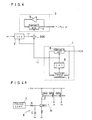
- Fig. 4 is a block diagram showing Fig. 1 block diagram in detail.
- the VCO 3 is constituted by current controlled variable band-pass filter (hereinafter, simply called as "variable BPF") 4 and a closed loop having the same phase and a fixed gain more than 1 through an amplifier 5.
- variable BPF current controlled variable band-pass filter
- the Fo control circuit 1 includes a variable all-pass filter (hereinafter, simply called as "variable APF") 6 which receives a clock signal CK having a fixed frequency, a phase comparator 7 which performs a phase comparison of an input and an output of the variable APF 6, and a low-pass filter (LPF) 8 which receives an output of the phase comparator 7 and controls the variable APF 6 by an output thereof.
- variable APF 6 is controlled by the output of the LPF 8, that is, an error signal which is the output of the phase comparator 7, a resonant point of the variable APF 6 can be in proportion to a frequency of the clock signal CK.
- the phase comparator 7 outputs the error signal of zero when a phase difference between the input and the output of the variable APF 6 is zero.
- the clock signal CK may be generated by a crystal oscillator (not shown).
- the LPF 8 which receives the output of the phase comparator 7 includes a resistor R and a capacitor C, and an output of the LPF 8 is applied to a base of a transistor Q91 constituting a converting circuit 9.
- the converting circuit 9 is a circuit for converting the output voltage of the LPF 8 into a current which is in proportion thereto.
- An emitter resistor is connected to an emitter of the transistor Q91 and a collector thereof is connected to the voltage source +Vcc through a transistor Q92.
- the transistor Q92 forms a current mirror circuit along with transistors Q93 and Q94. Therefore, the output voltage of the LPF 8 is converted into a control current Io by the converting circuit 9.
- variable APF 6 and the variable BPF 4 shown in Fig. 4 are formed in a single monolithic IC with the same circuit configuration, and more specifically, the same are constituted by utilizing a secondary variable filter which will be described later.
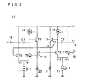
- Fig. 6 is a circuit diagram showing a principle of the variable filter.
- transistors T5 and T6 constitute a deferential pair, and emitters thereof are commonly connected to a constant current source circuit 11.
- the transistor T5 is supplied with the voltage +Vcc at a collector thereof, and a collector of the transistor T6 is connected to a constant current source circuit 12 and a base of a transistor T7 and to a terminal 15 through a capacitor C1.
- a current amount of the constant current source circuit 11 is set twice (2I1) a current amount I1 of the constant current source circuit 12.
- Transistors T9 and T10 also constitute a deferential pair, and emitters thereof are commonly connected to a constant current source circuit 13.
- the transistor T10 is supplied with the voltage +Vcc at a collector thereof, and a collector of the transistor T9 is connected to a constant current source circuit 14 and a base of a transistor T8 and to a terminal 18 through a capacitor C2.
- a base of the transistor T10 is connected to a terminal 19.
- a current amount of the constant current source circuit 13 is set twice (2I2) a current amount 12 of the constant current circuit 14.
- the transistor T7 is paired with the transistor T8 and the voltage +Vcc is applied to respective collectors thereof.
- an emitter of the transistor T7 is connected to bases of the transistors T6 and T9 and a terminal 16
- an emitter of the transistor T8 is connected to a base of the transistor T5 and a terminal 17.
- V1, V2, V3, V4 and V5 respectively correspond to voltage values of signals at the terminals 15, 16, 17, 18 and 19.
- variable filter 20 operates as a variable BPF.
- ⁇ o is an oscillation angle frequency of the BPF, which is variable by changing the current amounts 2I1 and 2I2 of the constant current source circuits 11 and 13.
- Q indicates a sharpness of the filter, which is also variable by changing the current amounts 2I1 and 1I2. In other words, by controlling the current amounts I1 and I2, it is possible to vary a characteristic of the variable BPF.
- V4 -Vin
- V2 Vout
- variable filter 20 shown in Fig. 6 operates as a variable APF, and a characteristic thereof is depend on the current amounts I1 and I2.
- V4 0
- V2 Vout
- the equation (21) indicates a transfer function of a band-elimination filter (BEF).
- variable filter shown in Fig. 6 operates as a variable BEF, and a characteristic thereof is dependent on the current amounts I1 and I2.
- V1 Vin
- V2 Vout
- variable filter 20 operates as a variable HPF, and a characteristic thereof is dependent on the current amounts I1 and I2.
- variable filter 20 operates as an LPF, and a characteristic thereof is dependent on the current amounts I1 and I2.
- variable filter 20 As described above, by applying the respective conditions without changing the circuit configuration, it is possible to operate the variable filter 20 as shown in Fig. 6 as a variable BPF or variable APF, and it is possible to control the characteristic of the filter by the current amounts I1 and I2.
- Fig. 7 is a circuit diagram showing a specific variable filter in which the current amounts I1 and I2 can be controlled by applying the principle of the variable filter 20 as shown in Fig. 6, wherein the constant current source circuits are constituted by current mirror circuits composed of transistors and resistors so that the current amounts of the constant current source circuits can be controlled in response to a current value of the control signal Io.
- the constant current source circuit 11 is constituted by transistors T11 and T12 connected in parallel with each other and a resistor 22 having a resistance value of r, and a control current signal Io which is supplied to a terminal 50 is injected to a collector of a transistor T21 which constitutes a current mirror circuit along with the transistors T11 and T12.
- the constant current source circuit 13 is also constituted by transistors T13 and T14 connected in parallel with each other and a resistor 23 having a resistance value of r, and a current having the same current amount as the control current signal which is injected to the collector of the transistor T21 flows into the transistors T13 and T14 which constitute a current mirror circuit along with the transistor T21.
- the constant current source circuit 12 is replaced with a current mirror circuit constituted by transistors T15 and T16 and a constant current source circuit constituted by a transistor T17 coupled to the transistor T16 and a resistor 24 having a resistance value of 2r, and a current amount thereof is controlled by the control current signal which is injected into a collector of the transistor T21.
- the constant current source circuit 14 is replaced with a current mirror circuit constituted by transistors T18 and T19 and a constant current source circuit constituted by a transistor T20 and a resistor 25 having a resistance value of 2r, and a current amount thereof is controlled by the control current signal which is injected to a collector of the transistor T21.
- resistors R1, R2, R3 and R4 are inserted to set a gain. Furthermore, the resistors R2 and R4 are connected to the ground in alternating current, and it is necessary to apply thereto a direct current bias such as Vcc/2 when such a circuit is to be operated actually.
- VCO voltage control oscillator
- variable filter 20 receives as the control signal therefor not the voltage but the current, and therefore, it is preferably that such a circuit is represented as a current controlled oscillator in practical; however, in this text, the circuit is represented as a voltage controlled oscillator (VCO) according to common usage because signals are generally sent and received between electronics equipments in a form of a voltage.
- VCO voltage controlled oscillator
- the terminals 15 and 16 are used as an input terminal which is supplied with a clock signal CK, the terminal 18 is supplied with a signal having a reverse polarity to the clock signal CK, the terminal 16 is used as the output terminal which is coupled to an input end of the phase comparator 7, and the terminal 50 is supplied with the current Io as the control signal, the variable filter 20 operates as the variable APF 6.
- variable APF 6 and the variable BPF 4 are formed in the same monolithic IC with the same circuit configuration as described above, a resonant point of the variable BPF 4 is in proportion to the clock signal CK as similar to that of the variable APF 6, and therefore, in a state where a frequency of the clock signal CK from the external is maintained at a constant value, the center frequency Fo also becomes constant value.
- Fo ( ⁇ q/KT) ⁇ (Io/C)
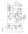
- a specific circuit configuration of the VCA 2 is shown in Fig. 5.
- the VCA 2 is also formed in the same monolithic IC as similar to the variable BPF 4 and the variable APF 6.
- the VCA 2 is mainly composed of a differential pair 40 which is constituted by a pair of NPN transistors Q1 and Q2 and arranged at outside, and a differential pair 41 which is coupled to the differential pair 40 in series and constituted by a pair of transistors Q3 and Q4 and arranged at inside.
- Collectors of the transistors Q1 and Q2 are respectively coupled to bases of the transistors Q3 and Q4 and to emitters of NPN transistors Q5 and Q6 which are connected to each other in a diode fashion.
- a transistor Q9 is inserted between the collectors of the transistors Q5 and Q6 and a line for the voltage +Vcc.
- emitters of the transistors Q1 and Q2 are coupled to both ends of a resistor Re and to collectors of transistors Q10 and Q11.
- the transistors Q10 and Q11 are transistors which constitute a constant current source circuit along with respective resistors 30 and 31, and respective bases thereof are coupled to a base of a transistor Q12 constituting a bias circuit 42 (described later) to constitute a current mirror circuit.
- Bases of the transistors Q1 and Q2 are coupled through resistors 32 and 33 to a line 36 which is biased at a predetermined voltage by a direct current voltage source 35, and especially, the base of the transistor Q1 is further connected to an input terminal 34 for inputting the modulation signal ⁇ v through a capacitor 37 for cutting-off a direct current component.
- Emitters of the transistors Q3 and Q4 are coupled to a collector of a transistor Q13 which constitutes a current mirror circuit along with a transistor Q14.
- a collector of the transistor Q14 is coupled to an input terminal 38 which is supplied with an output current Io of the Fo control circuit 1.
- collectors of the transistors Q3 and Q4 are coupled to collectors and bases of transistors Q15 and Q17 constitute current mirror circuits along with transistors Q16 and Q18, respectively, and a collector of the transistor Q16 is coupled to a collector and a base of a transistor Q19 which constitutes a current mirror circuit along with a transistor Q20, and a collector of the transistor Q18 is coupled to a collector of the transistor Q20 and an output terminal 39.
- the bias circuit 42 includes a PNP transistor Q7 having a base supplied with a fixed reference voltage Vr, an emitter connected to a voltage source line through a resistor 43, and a collector connected to the ground.
- the emitter of the transistor Q7 is coupled to a base of an NPN transistor Q8 having a collector coupled to a collector and a base of a transistor Q21.
- Bases of the transistor Q21 and a transistor Q22 are coupled to each other to constitute a current mirror circuit.
- a collector of the transistor Q22 is coupled to a collector and a base of a transistor Q12.
- a resistor R A is inserted between an emitter of the transistor Q8 and the ground, and a base of the transistor Q12 is coupled to the bases of the transistors Q10 and Q11 as described above to constitute a current mirror circuit.
- the current Io′ is equal to a collector current of the transistor Q8, according to a current mirror effect of the transistors Q21 and Q22, a collector current of the transistor Q12 is also equal to the current Io′, and further, according to a current mirror effect of the transistors Q10, Q11 and Q12, a collector current of each of the transistors Q10 and Q11 also becomes Io′.
- a gain of a differential pair is generally given by dividing a collector resistor (load) of transistors constituting the differential pair by an emitter resistor (load), that is, the collector resistor/the emitter resistor. Then, noting the differential pair 40, an input voltage is the modulation signal ⁇ v and an output voltage is collector voltages of the transistors Q1 and Q2 (respective collector voltages have reverse polarities to each other). Assuming that a differential resistor of the differential pair 40 is re3, an emitter load becomes 2re3 + R E .
- an input voltage is equal to each of the collector voltages of the transistors Q1 and Q2 which is the output voltage of the differential pair 40, and an output voltage is a voltage generated between the output terminal 39 and the line 36, and thus, if a load resistor Rf is inserted between the output terminal 39 and the line 36 as shown by a dotted line in Fig. 5, the output voltage becomes equal to a voltage generated between both ends of the load resistor Rf. Assuming that a differential resistor of the differential pair 41 is re4, an emitter load becomes 2re4.
- the transistors Q3 and Q4 function as a push-pull circuit, and therefore, a collector current of the transistor Q3 becomes a collector current of the transistor Q19 according to a current mirror effect of the transistors Q15 and Q16, and further, according to a current mirror effect of the transistors Q19 and Q20, the collector current of the transistor Q3 becomes a collector current of the transistor Q20.
- a collector current of the transistor Q4 becomes a collector current of the transistor Q18 according to a current mirror effect of the transistors Q17 and Q18.
- the collector current of the transistor Q4 increases, the collector current of the transistor Q3 decreases, and the collector current of the transistor Q18 becomes larger than the collector current of the transistor Q20, and thus a current amount due to an increase of the collector current of the transistor Q20 is outputted as an output current ⁇ i.
- the collector current of the transistor Q3 increases, the collector current of the transistor Q4 decreases, the collector current of the transistor Q18 becomes smaller than the collector current of the transistor Q20, and thus, a current amount for compensating a lack due to a decrease of the collector current of the transistor Q20 flows into the terminal 39 inversely. Therefore, the load resistor Rf contributes to the collector load of the transistors Q3 and Q4, and therefore, the collector load of the differential pair 41 becomes 2Rf.
- a voltage gain A2 of the differential pair 41 is given by the following equation (29).
- the VCA 2 of this embodiment shown is actually a V-I converter of a current controlled gain type, and therefore, a gain A of the V-I converter is a product of a voltage gain A1 by the V-I gain A3, and therefore, represented by the following equation (32).
- the equations (33) and (30) are substituted for the equation (32), the following equation (34) is obtainable.
- the equation (40) is the same as the equation (8), and therefore, by constructing the VCA 2 as shown in Fig. 5 and setting m to be coincident with a target value, a frequency modulated signal having a frequency deviation amount ⁇ f which is not dependent upon variations of capacitors of VCO and a temperature drift thereof can be outputted.
- a combination of the VCO 3 and VCA 2 of Fig. 4 can be regarded as a sort of a VCO, and therefore, if such a VCO is used as a PLL (Phase Locked Loop) circuit, an FM demodulator in which a demodulation sensitivity is determined by the above described equation (8) is obtained.
- a sound signal recording circuit of an 8mm VTR or the like an FM modulator becomes necessary in recording and an FM demodulator becomes necessary in playing, and therefore, by applying the above described embodiment to such an FM demodulator, it is possible to obtain an FM modulation and demodulation system of adjustment free.
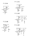
- Fig. 9 is a block diagram showing another embodiment in accordance with the present invention.
- the center frequency control circuit 1 is constituted by the variable APF 6, the phase comparator 7 and the LPF 8.
- a center frequency control circuit 10 is constituted as a PLL which includes a crystal oscillator 101. More specifically, an output of a crystal oscillator 101 is frequency-divided by 1/M by a programmable frequency divider 102 and then inputted to a phase comparator 106.
- the direct current voltage form the PLL, that is, the center frequency control circuit 10 controls a center frequency of the VCO 3 and an amplitude of an alternating current signal from the VCA 2, that is, a frequency deviation amount.
- a frequency modulator of adjustment free is described.
- a rough adjustment may be performed by a variable resistor and a fine adjustment may be performed by a PLL.
- a center frequency control circuit 10′ includes a variable resistor 106 and a voltage from the variable resistor 106 is applied to a base of a transistor Q101.
- the transistor Q101 constitutes a conversion circuit as similar to the transistor Q91 of Fig. 4A, which converts the output voltage of the variable resistor 106 into a current.
- transistors Q102, Q103 and Q104 constitute a current mirror circuit. Therefore, respective output currents of the transistor Q103 and Q104 are in proportion to the output voltage of the variable resistor 106.
- the output currents of the transistors Q103 and Q104 are applied to the VCA 2 and the adder 300 respectively as similar to Fig. 4 embodiment. Therefore, in this embodiment shown, the center frequency and the frequency deviation amount of the VCO 3 can be controlled by only the center frequency control circuit 10′, that is, variable resistor 106.
- the center frequency control circuit 10 shown in Fig. 9 can be used.
- the output of such a Fo control circuit 10 is given to only the VCO 3 and is not given to the VCA 2.
Landscapes
- Networks Using Active Elements (AREA)
- Stabilization Of Oscillater, Synchronisation, Frequency Synthesizers (AREA)
- Digital Transmission Methods That Use Modulated Carrier Waves (AREA)
- Amplitude Modulation (AREA)
Applications Claiming Priority (2)
| Application Number | Priority Date | Filing Date | Title |
|---|---|---|---|
| JP187809/89 | 1989-07-20 | ||
| JP1187809A JP2542928B2 (ja) | 1989-07-20 | 1989-07-20 | Fm変調器 |
Publications (3)
| Publication Number | Publication Date |
|---|---|
| EP0409277A2 true EP0409277A2 (de) | 1991-01-23 |
| EP0409277A3 EP0409277A3 (en) | 1991-05-29 |
| EP0409277B1 EP0409277B1 (de) | 1995-09-27 |
Family
ID=16212624
Family Applications (1)
| Application Number | Title | Priority Date | Filing Date |
|---|---|---|---|
| EP90113978A Expired - Lifetime EP0409277B1 (de) | 1989-07-20 | 1990-07-20 | Frequenzmodulator |
Country Status (6)
| Country | Link |
|---|---|
| US (1) | US4994766A (de) |
| EP (1) | EP0409277B1 (de) |
| JP (1) | JP2542928B2 (de) |
| KR (1) | KR0146364B1 (de) |
| CA (1) | CA2021335C (de) |
| DE (1) | DE69022655T2 (de) |
Cited By (2)
| Publication number | Priority date | Publication date | Assignee | Title |
|---|---|---|---|---|
| WO1996037987A1 (en) * | 1995-05-22 | 1996-11-28 | Telefonaktiebolaget Lm Ericsson | Method and device for phase-modulated signals |
| WO1998000906A1 (en) * | 1996-06-28 | 1998-01-08 | Telefonaktiebolaget Lm Ericsson (Publ) | Method and device for use with phase modulated signals |
Families Citing this family (6)
| Publication number | Priority date | Publication date | Assignee | Title |
|---|---|---|---|---|
| US6141425A (en) * | 1996-09-30 | 2000-10-31 | Sony Corporation | Sound quality adjustment circuit |
| DE10258627B4 (de) * | 2002-12-16 | 2007-08-30 | Daimlerchrysler Ag | Kraftfahrzeug mit einer Fronthaube |
| US7349488B1 (en) * | 2003-04-10 | 2008-03-25 | Xilinx, Inc. | Frequency shift keying signaling for integrated circuits |
| KR100812228B1 (ko) | 2007-04-30 | 2008-03-13 | 한국전자통신연구원 | 밀러 효과를 이용한 이중 평형 주파수 혼합기 |
| JPWO2009078112A1 (ja) | 2007-12-19 | 2011-04-28 | パナソニック株式会社 | 演算増幅器,パイプライン型ad変換器 |
| KR101822068B1 (ko) * | 2011-11-23 | 2018-01-26 | 페어차일드코리아반도체 주식회사 | 스위치 제어 방법, 스위치 제어기 및 이를 포함하는 컨버터 |
Family Cites Families (6)
| Publication number | Priority date | Publication date | Assignee | Title |
|---|---|---|---|---|
| US3500248A (en) * | 1967-03-08 | 1970-03-10 | Gates Radio Co | Low frequency modulation network |
| GB2045024B (en) * | 1979-03-22 | 1983-03-23 | Marconi Co Ltd | Frequency and amplitude control of frequency sources |
| FR2554656B1 (fr) * | 1983-11-04 | 1986-06-27 | Lgt Lab Gen Telecomm | Emetteur a modulation de frequence applicable a la radiodiffusion fm |
| JPS6372204A (ja) * | 1986-09-12 | 1988-04-01 | Matsushita Electric Ind Co Ltd | 電圧制御発振器の変調感度補正回路 |
| US4706047A (en) * | 1986-12-01 | 1987-11-10 | Ford Aerospace & Communications Corporation | Frequency extended digitally generated FM |
| JPH01170204A (ja) * | 1987-12-25 | 1989-07-05 | Hitachi Ltd | 変調回路 |
-
1989
- 1989-07-20 JP JP1187809A patent/JP2542928B2/ja not_active Expired - Fee Related
-
1990
- 1990-07-17 CA CA002021335A patent/CA2021335C/en not_active Expired - Fee Related
- 1990-07-19 US US07/554,497 patent/US4994766A/en not_active Expired - Lifetime
- 1990-07-19 KR KR1019900010960A patent/KR0146364B1/ko not_active Expired - Fee Related
- 1990-07-20 EP EP90113978A patent/EP0409277B1/de not_active Expired - Lifetime
- 1990-07-20 DE DE69022655T patent/DE69022655T2/de not_active Expired - Fee Related
Cited By (6)
| Publication number | Priority date | Publication date | Assignee | Title |
|---|---|---|---|---|
| WO1996037987A1 (en) * | 1995-05-22 | 1996-11-28 | Telefonaktiebolaget Lm Ericsson | Method and device for phase-modulated signals |
| US5751187A (en) * | 1995-05-22 | 1998-05-12 | Telefonaktiebolaget Lm Ericsson | Method and device for phase-modulated signals |
| CN1085920C (zh) * | 1995-05-22 | 2002-05-29 | 艾利森电话股份有限公司 | 相位调制信号的方法和装置 |
| WO1998000906A1 (en) * | 1996-06-28 | 1998-01-08 | Telefonaktiebolaget Lm Ericsson (Publ) | Method and device for use with phase modulated signals |
| US6091789A (en) * | 1996-06-28 | 2000-07-18 | Telefonaktiebolaget Lm Ericsson | Method and device for phase modulated signals |
| CN1111943C (zh) * | 1996-06-28 | 2003-06-18 | 艾利森电话股份有限公司 | 供相位调制信号使用的方法和装置 |
Also Published As
| Publication number | Publication date |
|---|---|
| JP2542928B2 (ja) | 1996-10-09 |
| KR910003912A (ko) | 1991-02-28 |
| KR0146364B1 (ko) | 1998-12-01 |
| JPH0352405A (ja) | 1991-03-06 |
| EP0409277A3 (en) | 1991-05-29 |
| EP0409277B1 (de) | 1995-09-27 |
| DE69022655T2 (de) | 1996-04-11 |
| DE69022655D1 (de) | 1995-11-02 |
| CA2021335C (en) | 1999-07-13 |
| CA2021335A1 (en) | 1991-01-21 |
| US4994766A (en) | 1991-02-19 |
Similar Documents
| Publication | Publication Date | Title |
|---|---|---|
| US6404277B1 (en) | Gm-C tuning circuit with filter configuration | |
| EP0393717A2 (de) | Aktive Filterschaltung | |
| EP0409278B1 (de) | Monostabiler Multivibrator | |
| JPH0787332B2 (ja) | フイルタ回路の時定数自動調整回路 | |
| JPH07245546A (ja) | アクティブローパスフィルタ | |
| US4525686A (en) | Phase-locked loop circuit with variable bandwidth filter | |
| CN1069463C (zh) | 电压控制振荡器 | |
| EP0409277B1 (de) | Frequenzmodulator | |
| US4937537A (en) | Circuit arrangement for compensating for the thermal drift of a phase detector | |
| US5909644A (en) | AM radio receiver | |
| CN1639979A (zh) | 电荷泵 | |
| US5343170A (en) | Voltage controlled oscillator provided with negative feedback biasing | |
| GB2202700A (en) | A phase-locked loop fm detection system | |
| US20060077009A1 (en) | Frequency generator with a phase locked loop | |
| EP1402642B1 (de) | Frequenzregelkreis, taktwiederherstellungsschaltung und empfänger | |
| JP2937316B2 (ja) | Fm変調器 | |
| JPH0691413B2 (ja) | リアクタンス制御回路 | |
| JPS6374301A (ja) | 周波数制御回路 | |
| JP2794055B2 (ja) | Cr定数制御回路 | |
| KR0163900B1 (ko) | 증폭단이 내장된 위상 동기 루프 방식의 에프엠 검파 회로 | |
| JP2774563B2 (ja) | Fm映像信号検波回路 | |
| JPH0323007B2 (de) | ||
| JPH06310982A (ja) | 位相変移回路 | |
| JPH06338789A (ja) | 位相同期回路 | |
| JPH0969753A (ja) | 信号処理回路 |
Legal Events
| Date | Code | Title | Description |
|---|---|---|---|
| PUAI | Public reference made under article 153(3) epc to a published international application that has entered the european phase |
Free format text: ORIGINAL CODE: 0009012 |
|
| AK | Designated contracting states |
Kind code of ref document: A2 Designated state(s): DE ES FR GB IT |
|
| 17P | Request for examination filed |
Effective date: 19901228 |
|
| PUAL | Search report despatched |
Free format text: ORIGINAL CODE: 0009013 |
|
| AK | Designated contracting states |
Kind code of ref document: A3 Designated state(s): DE ES FR GB IT |
|
| 17Q | First examination report despatched |
Effective date: 19931129 |
|
| GRAA | (expected) grant |
Free format text: ORIGINAL CODE: 0009210 |
|
| AK | Designated contracting states |
Kind code of ref document: B1 Designated state(s): DE ES FR GB IT |
|
| PG25 | Lapsed in a contracting state [announced via postgrant information from national office to epo] |
Ref country code: IT Free format text: LAPSE BECAUSE OF FAILURE TO SUBMIT A TRANSLATION OF THE DESCRIPTION OR TO PAY THE FEE WITHIN THE PRESCRIBED TIME-LIMIT;WARNING: LAPSES OF ITALIAN PATENTS WITH EFFECTIVE DATE BEFORE 2007 MAY HAVE OCCURRED AT ANY TIME BEFORE 2007. THE CORRECT EFFECTIVE DATE MAY BE DIFFERENT FROM THE ONE RECORDED. Effective date: 19950927 Ref country code: ES Free format text: THE PATENT HAS BEEN ANNULLED BY A DECISION OF A NATIONAL AUTHORITY Effective date: 19950927 Ref country code: FR Effective date: 19950927 |
|
| REF | Corresponds to: |
Ref document number: 69022655 Country of ref document: DE Date of ref document: 19951102 |
|
| EN | Fr: translation not filed | ||
| PLBE | No opposition filed within time limit |
Free format text: ORIGINAL CODE: 0009261 |
|
| STAA | Information on the status of an ep patent application or granted ep patent |
Free format text: STATUS: NO OPPOSITION FILED WITHIN TIME LIMIT |
|
| 26N | No opposition filed | ||
| REG | Reference to a national code |
Ref country code: GB Ref legal event code: IF02 |
|
| PGFP | Annual fee paid to national office [announced via postgrant information from national office to epo] |
Ref country code: GB Payment date: 20040714 Year of fee payment: 15 |
|
| PGFP | Annual fee paid to national office [announced via postgrant information from national office to epo] |
Ref country code: DE Payment date: 20040729 Year of fee payment: 15 |
|
| PG25 | Lapsed in a contracting state [announced via postgrant information from national office to epo] |
Ref country code: GB Free format text: LAPSE BECAUSE OF NON-PAYMENT OF DUE FEES Effective date: 20050720 |
|
| PG25 | Lapsed in a contracting state [announced via postgrant information from national office to epo] |
Ref country code: DE Free format text: LAPSE BECAUSE OF NON-PAYMENT OF DUE FEES Effective date: 20060201 |
|
| GBPC | Gb: european patent ceased through non-payment of renewal fee |
Effective date: 20050720 |