EP0407685A2 - Verfahren und Vorrichtung zur Untersuchung von Lötstellen mittels eines röntgenfluoroskopischen Bildes - Google Patents
Verfahren und Vorrichtung zur Untersuchung von Lötstellen mittels eines röntgenfluoroskopischen Bildes Download PDFInfo
- Publication number
- EP0407685A2 EP0407685A2 EP90103236A EP90103236A EP0407685A2 EP 0407685 A2 EP0407685 A2 EP 0407685A2 EP 90103236 A EP90103236 A EP 90103236A EP 90103236 A EP90103236 A EP 90103236A EP 0407685 A2 EP0407685 A2 EP 0407685A2
- Authority
- EP
- European Patent Office
- Prior art keywords
- solder joint
- fluoroscopic image
- ray fluoroscopic
- ray
- inspecting
- Prior art date
- Legal status (The legal status is an assumption and is not a legal conclusion. Google has not performed a legal analysis and makes no representation as to the accuracy of the status listed.)
- Granted
Links
Images


Classifications
-
- G—PHYSICS
- G01—MEASURING; TESTING
- G01N—INVESTIGATING OR ANALYSING MATERIALS BY DETERMINING THEIR CHEMICAL OR PHYSICAL PROPERTIES
- G01N23/00—Investigating or analysing materials by the use of wave or particle radiation, e.g. X-rays or neutrons, not covered by groups G01N3/00 – G01N17/00, G01N21/00 or G01N22/00
- G01N23/02—Investigating or analysing materials by the use of wave or particle radiation, e.g. X-rays or neutrons, not covered by groups G01N3/00 – G01N17/00, G01N21/00 or G01N22/00 by transmitting the radiation through the material
- G01N23/04—Investigating or analysing materials by the use of wave or particle radiation, e.g. X-rays or neutrons, not covered by groups G01N3/00 – G01N17/00, G01N21/00 or G01N22/00 by transmitting the radiation through the material and forming images of the material
- G01N23/043—Investigating or analysing materials by the use of wave or particle radiation, e.g. X-rays or neutrons, not covered by groups G01N3/00 – G01N17/00, G01N21/00 or G01N22/00 by transmitting the radiation through the material and forming images of the material using fluoroscopic examination, with visual observation or video transmission of fluoroscopic images
-
- H—ELECTRICITY
- H05—ELECTRIC TECHNIQUES NOT OTHERWISE PROVIDED FOR
- H05K—PRINTED CIRCUITS; CASINGS OR CONSTRUCTIONAL DETAILS OF ELECTRIC APPARATUS; MANUFACTURE OF ASSEMBLAGES OF ELECTRICAL COMPONENTS
- H05K13/00—Apparatus or processes specially adapted for manufacturing or adjusting assemblages of electric components
- H05K13/08—Monitoring manufacture of assemblages
- H05K13/082—Integration of non-optical monitoring devices, i.e. using non-optical inspection means, e.g. electrical means, mechanical means or X-rays
Definitions
- This invention relates to a method for inspection of solder joints by X-ray fluoroscopic image, apparatus therefor and mounting construction of electronic parts on a board.
- the solder joints become a fine configuration as described above, and therefore, locating to a solder joint to be inspected need be done with high accuracy.
- the locating to the solder joint is accomplished in dependence of mechanical accuracy from a positioned obtained by teaching. Therefore, the mechanical accuracy is affected by the accuracy of teaching, the pattern accuracy of a printed circuit board to be inspected, and the mechanical accuracy. It has been difficult to detect a fine solder joint with high accuracy.
- the brightness of a transmitted X-ray image of a solder joint corresponds to the thickness of the solder joint.
- a position of the solder joint cannot be decided with good accuracy for the reason described later, and the brightness only in a specific area within the solder joint is used as a reference value for comparison. Only the thickness of a part of the solder joint is decided. Also, no consideration has been given to the quantity of solder and a cubic shape of fillet.
- lead lead frame
- an X-ray is irradiated on an object to be inspected in which a lead of an electronic part is soldered to a substrate located by a specimen state to obtain a signal of the X-ray fluoroscopic image, a position of a solder joint as an object to be inspected is extracted by the X-ray fluoroscopic image, an inspection area is set every solder joint in accordance with the position information, and the signal of the X-ray fluoroscopic image is evaluated every inspection area thus set to decide a defect.
- the signal of the detected X-ray fluoroscopic image is subjected to shading compensation, a concentration level is subjected to logarithmic conversion, and thereafter, an addition of image, so-called distribution of projection is prepared in the lead row direction and the lead tip direction, and a position of each solder joint is detected from a waveform of the distribution of projection.
- a fine solder joint can be automatically detected in position with high accuracy from the image of the X-ray fluoroscopic image of a solder joint in which an IC or the like is mounted, thus coping with the high density and miniaturized substrate (printed circuit board). Furthermore, the defect decision with high reliability can be carried out by deciding a defect every solder joint detected.
- the width or spacing of a solder joint is compared with a reference value to thereby evaluate the signal of the X-ray fluoroscopic image to decide a defect.
- an image is integrated every solder joint detected to thereby decide the quantity of solder to decide a defect.
- a deviation in lead is decided from the width in the lead row direction of the solder joint, and the presence or absence of solder between the solder joints is decided from a binary image signal between the solder joints to decide a defect.
- a fillet shape is decided from the primary image in the lead tip direction in the central portion of the solder joint.
- a signal of the detected X-ray fluoroscopic image is compared with signals of a plurality of good reference images to decide a fillet shape.
- the signals of the good reference images are set with high accuracy and effectively. More specifically, a number of good solder joints are prepared. The solder joints are detected, and a number of primary images in the lead tip direction are extracted according to the positions thereof.
- Several typical waveforms are selected by clustering from signals of a number of primary images (waveforms) thus obtained to set the good reference images.
- the signals of the good solder joints serving as a reference can be automatically selected, and signals of a plurality of good solder joints corresponding to soldering variations can be prepared.
- the defect decision based on the fillet shape with high reliability can be carried out.
- the vertical direction of a substrate having solder joints on the inside and outside thereof is inclined with respect to an optical axis of an X-ray detection system so that signals of the X-ray fluoroscopic image of the inside and outside solder joints are not superimposed so as to detect the signals of the X-ray fluoroscopic image.
- the solder joints in the inside and outside of the substrate can be separated and detected.
- the solder joints can be detected without being affected by the deterioration of a dynamic range detected, and the inside and outside solder joints can be inspected with high accuracy.
- the inspection apparatus is provided with shutter means for cutting off an X-ray irradiated on an IC out of LSI and the like mounted on the substrate and filter means for changing the distribution of waveform of the irradiated X-ray, whereby the quantity of irradiation of X-rays to the IC can be reduced to reduce a damage thereto.
- a portion between IC leads is divided into a plurality of decision areas according to the presence or absence or kind of a lead image of IC, and in an area where no lead image is present, an image of a solder bridge is obtained at a darker level than a material of a printed cicuit board, according to the present invention, a threshold which separates from the material portion to actualize only the solder bridge is used to form a binary image and decide the presence or absence of the solder bridge.
- a threshold which actualizes a level below a lead frame image is used to form a binary image, and the presence or absence of a soldering bridge or a soldering ball is decided. Furthermore, in an area in which a wiring pattern of a lead is detected, a threshold which separates from a material portion of a printed board, and a soldering image as well as a lead are simultaneously actualized is used to form a binary image, and the number of patterns is obtained from the signal of the binary image.
- a distribution of image projection (addition) in that area is obtained, and a pad position of the solder joint is detected from said distribution.
- a decision area is provided between the pads on the X-ray image on the basis of a result of detected position of the pad, and evaluation of a binary image with respect to the IC lead image forced into the decision area is effected, on the basis of which a decision of deviation in position of the IC lead is effected.
- a reference position recognition pattern is provided in advance on an inspection circuit board, and a decision area is set between pads of a solder joint on the basis of the result of recognition of a position of the X-ray image with respect to said pattern.
- this recognition of a reference position is effected paying attention to a clearance pattern or the like detected as a high contrast pattern on the X-ray image of a circuit board to achieve the aforesaid object.
- FIG. 1 a printed circuit board (PCB) 2 with a part 1 mounted by soldering is placed on a XY ⁇ stage composed of X, Y and ⁇ stages.
- a micro-focusx-ray source 4 an image intensifier 5 as an X-ray image detector and a TV camera 6 are mounted on a ⁇ stage 7 which rotates about r in a direction of ⁇ .
- the X-ray is obliquely irradiated on the PCB 2 so that a transmitted X-ray image can be detected.
- An X-ray control unit 71 controls voltage of the X-ray source 4, current thereof, focussing, generation of X-ray, etc.
- the X-ray source 4 can be controlled in a direction of z.
- a stage control unit 9 actuates the XY ⁇ stage 3 and the ⁇ stage 7according to a command of the CPU 8.
- a picture processing unit 10 receives a video signal from the TV camera 6, and processes an image according to a command of the CPU 8. As the result, the CPU 8 decides a defect of each solder joint.
- FIG. 3 shows typical examples of surface mounted parts which comprise main objects in the present invention. That is, FIG. 3(a) shows Gull Wing lead type (abridged as SOP), FIG. 3(b) Quad Flat Package type (QFP), FIG. 3(c) Mini Square Package type (MSP) with Butt-joint lead, FIG. 3(d) Plastic Leadless Chip Carrier type (PLCC) with J-lead, and FIG. 3(e) Leadless Chip type which is a lead-less type.
- Gull Wing lead type (abridged as SOP)
- QFP Quad Flat Package type
- MSP Mini Square Package type
- PLCC Plastic Leadless Chip Carrier type
- FIG. 3(e) Leadless Chip type which is a lead-less type.
- FIG. 4 shows a section of a solder joint of the above-described type.
- FIG. 4(a) shows (SOP) or (QFP) type
- FIG. 4(b) PLCC
- FIG. 4(c) MSP
- FIG. 4(d) LCC
- reference numeral 30 designates a solder, 31 a substrate pad, 32 a lead, 33 a package, and 35 a J lead.
- the lead will be generally referred to as "lead 32" except the special case, including the J lead.
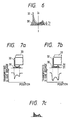
- FIG. 5 shows examples of defects to be inspected.
- FIG. 5(a) shows the case of a good product, in which 30 is a solder, 31 a substrade pad and 32 a lead.
- FIG. 5(b) shows the case where the lead 32 is apart (lifted) from the solder 30.
- FIG. 5(c) shows the case where a fillet is small.
- FIG. 5 (d) shows the case where a lead 35 is considerably deviated from the substrate pad 31.
- FIG. 5(e) shows the case where leads 32 and 32′ adjacent to each other form a bridge by a solder 30′.
- FIG. 6 is a view for explaining formation of a transmitted X-ray image in J lead.
- I o be the intensity of incident X-ray
- t1 be the thickness of a solder joint
- t2 be the thickness of those other than the solder, for example, the thickness of lead
- ⁇ 1 be the X-ray absorption coefficient of solder
- ⁇ 2 be the X-ray absorption coefficient of those (mainly, lead and wiring pattern) other than solder
- Equation (3) is obtained: I o and ⁇ 1 are constant. ⁇ 2 and t2 change in value according to the difference in a wiring pattern of a printed circuit board. However, it is a value mostly determined according to a part and a position of a solder joint since the thickness of the wiring pattern is small, scores of Um. If lnI is integrated at the solder joint, the value ( ⁇ t1) obtained by integrating t1, that is, the value corresponding to the amount of solder can be calculated. In this case, When the lead is deviated, the width of the solder joint becomes widened. Thereby, a deviated lead can be extracted by deciding the width of the solder joint.
- the solder Since the solder is darker than the other portions, it can be extracted as a binary image by binarizing it with a suitable threshold. Thereby, the binary image is projected in the lead tip direction between the solder joints whereby defects such as a bridge, a soldering ball, etc. can be extracted.
- the X-ray fluoroscopic image when solder is not present is obtained by use of Equation (2) as follows: From (2) - (5), That is, a difference of an image between the case where "solder is present" as shown in FIG. 7a and the case where "solder is absent” as shown in FIG. 7b is obtained, whereby a fillet shape as shown in FIG. 7c can be extracted as a distribution of the solder thickness t1. Accordingly, in the aforementioned decision of the amount of -solder, the lifted lead as in "the lead is lifted despite the fact that the amount of solder is normal" can be detected.
- FIG. 8 A specific structural example of the picture processing unit 10 (shown in FIG. 1) for effecting the processing as described above is shown in FIG. 8.
- a video signal from a TV camera 6 is converted into a digital value by an A/D converter 11, after which it is inputted into a memory 14 through a shading compensation circuit 12 and a logarithmic conversion circuit 13.
- the shading compensation is to compensate a variation in video level despite the same brightness in the central portion and in the circumferential portion of a picture plane.
- Detecting images (called white images) W (i, j) when a material to be inspected is not present and detecting imges (called black images) B (i, j) when the X-ray is not generated are used to obtain by detecting images g (i, j). Then, the detected image is normalized with respect to the white image and black image.
- FIG. 9 A specific structural example is shown in FIG. 9. In the FIG. 9, the logarithmic conversion is included, and the image after logarithmic conversion is outputted as 1 f(i, j).
- a difference between a detection image signal 15, an output of a black image memory 16, an output of a white image memory 17 and an output of a black image memory 16 is obtained by subtracters 18 and 19.
- Outputs are combined (g-B)(W-B) as a bit string by a combiner 20.
- the output of 20 is addressed to read the content of a memory 21 for transformation table 21 to output the image f(i, j) (hereinafter referred to as 22) after transformation.
- the content of the memory 21 for transformation table is stored upon logarithmic conversion in an address in which a value of the left side of Equation (7) is determined by a denomi nator and a numerator of the right side thereof.
- a binarization circuit 25 is designed so that a threshold (a solder or lead portion is detected as an X-ray image to be darker than other portions) for actualizing a solder (such as a bridge) or lead present between solder joints is designated by the CPU 8 to binarize the image stored in the memory 14.
- a projection circuit 26 prepares a projection in the lead tip direction with respect to the binary image in an area designated by the CPU 8.
- the CPU 8 controls the stages 3 and 7 (shown in FIG. 1), locates a printed circuit board and inputs an X-ray fluoroscopic image into the memory 14 in accordance with positional inforamtion of the solder joint obtained from teaching or design information. Subsequently, the CPU 8 designates projection areas with respect to the horizontal and vertical projection circuits 23 and 24 to prepare projections, analyze projections and detect the position of the solder joint. The CPU 8 analyzes the projections obtained by the 23 and 24 and the image inputted into the memory 14 in accordance with the positon of the detected solder joint to extract a defect of each solder joint. The projection of the bianary image is obtained by the projection circuit 26, and a defect between the solder joints is extracted by how the obtained projection is analyzed.
- FIG. 12a shows a section of a solder joint of J lead
- FIG. 13b shows a variation in brightness of X-ray image in the lead tip direction. The brightness of the X-ray image becomes dark as the solder thickness increases.
- the X-ray image becomes darkest at a raised portion of the J lead.
- the lead is smaller in absorption of X-ray than the solder, the X-ray image is darker than that of a portion where the solder thickness is maximum.
- the distribution H(j) of a brightness addition value of horizontal projection as shown in FIG. 14b is obtained.
- the CPU 8 receives the H(j) and obtains points of intersection js and je between the threshold Thl and the brightness addition value H(j) as shown in FIG. 15 to set positions of the vertical solder joints.
- the threshold Thl is set in advance, or a value is used which is subjected to interior division with a ratio wherein the maximum and mininum values of the inputted horizontal projection H(j) are set in advance.
- the distribution of brightness (addition value) as shown in FIG. 16b is obtained.
- the CPU 8 shown in FIG. 8 inputs the vertical projection V(i) to obtain the threshold Th2 and points of intersections is1, ie1 to ie4, is4 of V(i) to serve as the solder joint in the horizontal direction i.
- the threshold Th2 is set similarly to the Th1.
- FIG. 18 shows an example of a sectional shape of a deviated lead
- (b) thereof is a plan view showing a solder joint obtained by an X-ray fluoroscopic image.
- i sn ⁇ i en (n 1 ⁇ 4) obtained in FIG. 17 -are compared with good solder joint to thereby detect a deviated lead.
- the X-ray fluoroscopic image has a brightness corresponding to the thickness of material.
- one to which image value is added corresponds to the amount of solder in the solder joint.
- V(i) is integrated, a value corresponding to the amount of solder which corresponds to each solder joint can be obtained. This can be compared with a good one to thereby extract a surplus or short of solder.
- FIG. 19 shows an example of a lifted lead in which the amount of solder is normal but lead is lifted.
- a fillet shape is decided to detect such a defect.
- the horizontal and vertical projection circuits 23 and 24 shown in FIG. 8 are used with respect to the X-ray image when solder is not present to detect a solder joint. Since the lead portion has no solder but the lead thickness is thicker than other portions and is Fe or Cu, it has a darker image value than other portions. Therefore, as far as the lead row (arrangement) direction is concerned, substantially the same position as the good product is detected. Also with respect to the lead tip direction, as shown in FIG. 20a and 20b, a middle point jc (FIG.
- a similar image data is inputted from the CPU 8 to the memory 14 in each solder joint from the image of an object to be inspected to obtain a difference from the image data without solder, whereby the fillet shape is extracted as in FIG. 21.
- a defect is decided by the fillet shape when a difference between a good fillet shape and a fillet shape of an object to be inspected exceeds a set value.
- FIG. 21a1, FIG. 21b1 and FIG. 21c1 are similar to those of FIG. 7a to FIG. 7c as previously mentioned.
- a fillet shape shown in FIG. 21c1 is extracted as a distribution of the solder thickness t1, s .
- This system is provided with one having a fillet having a good solder joint, that is, "good fillet shape”.
- FIG. 21b3 When a difference between a pattern having a solder joint with a good fillet shape as shown in FIG. 21b1 and a pattern having a solder joint of an object to be inspected shown in FIG. 21b2 is obtained, it results as shown in FIG. 21b3.
- the thus obtained pattern is similar in shape to that shown in FIG. 21c4. In this case, it is not at all necessary to compare them one by one with that of non-soldering, and therefore, the decision of a fillet shape is materially simplified, in which respect, inspection means having an outstanding effect is obtained.
- a number of good waveforms are collected, fillet waveforms GW1 to GW M of a number of good products are subjected to clustering, those similar in shape are collected, the whole good waveform is divided into a few classes, and a typical good waveform is automatically extracted every class.
- the algorithm of clustering includes a so-called K average algorithm. A system for automatically extracting a good waveform by use of the aforesaid algorithm is described below.
- WM1 - WM R designate means for average of waveform, S1 - S N reference waveforms for decision, W a detection fillet shape obtained by the reference waveforms S1 - SN, and mim
- ⁇ (j 1 to N) defect decision condition with ⁇ as the decision threshold, respectively.
- K average algorithm n number of good waveforms are divided into K classes. The following steps are carried out.
- FIG. 23 a position of a solder joint is extracted from the X-ray image similar to the inspection. A waveform signal of the solder joint is inputted into the CPU 8 on the basis of the obtained result. These waveforms are sequentially stored in the memory. After a predetermined number of waveforms have been collected, good waveforms are selected by clustering.
- the one surface mounted substrate has been used, it is to be noted that an image of a solder joint is detected so that a substrate is tilted as shown in FIG. 25 so that the inside and outside solder joints are not overlapped, whereby similar processing can be made for a dual mounted substrate.
- the fillet decision has been carried out in the lead tip direction, it is to be noted that the decision may be made in the lead row direction on the basis of the position detection of the solder joint.
- defects of solder joint include a bridge, a soldering ball and the like produced between solder joints.
- a binary image of an X-ray fluoroscopic image is obtained by the binarization circuit 25 shown in FIG. 8, and a binary image is projected in a vertical direction between the solder joints obtained in FIGS. 15 and 17.
- FIG. 24(a) shows a binary image when a soldering ball and a soldering brige is present
- FIG. 24(b) shows a projection
- FIG. 24(c) shows a waveform in which a projection is binarized by threshold Th3.
- the CPU 8 receives a projection obtained by the projection generating circuit 26, and after the projection has been binarized, the length of "0" from the end between the solder joints is obtained to decide a defect.
- the horizontal and vertical projection value are obtained with respect to the X-ray fluoroscopic image of the solder joint whereby the position of the individual solder joint is extracted, and defects such as a short of solder, lifted lead, bridge, soldering ball, etc are extracted in accordance with the extracted position.
- the dual mounting as shown in FIG. 25 is often used.
- the decision of a deviated lead, bridge and soldering ball may be carried out by the aforementioned system, but there is a possibility that the inside and outside solders are overlapped, the dynamic range of detection is short, and the sensitivity of detection of surplus or short of solder lowers. As shown in FIG.
- FIG. 26 shows an example of the thus detected X-ray fluoroscopic image.
- FIG. 26(a) shows the case where the dual mounted substrate is tilted
- FIG. 26(b) shows the X-ray fluoroscopic image.
- the FIG. 27 configuration results, and only a set of inside and outside solder joints can be separated in the system shown in FIG. 17.
- a middle point ic n beteen is n and ie n is obtained as shown in FIG.
- FIG. 28 shows a flow of image processing when a substrate is not tilted such as the case of one surface mounting (when a substrate is not tilted at ⁇ )
- FIG. 29 shows a flow of image processing when a substrate is tilted (when a substrate is tilted at ⁇ )
- FIG. 30 shows a flow of inspection of a dual mounted substrate.
- the phase termed refers to a quadrant (phase) of a lead of a solder joint of an IC (part) 1 to be inspected.
- clockwise numbers F1 to F4 are indicated.
- Reference numerals 101, 101′ designate the operation of TV camera 6 and A/D converter 11 shown in FIG. 8; 102, 102′ the operation of the shading compensation circuit 12; and 103, 103′ the operation of the logarithmic conversion circuit 13.
- the image is inputted into the memory 14 by 103 and 103′.
- 104 and 104′ and 105, 105′ designate the solder joint extraction processing in which the CPU 8 analyzes the horizontal and vertical projections prepared by 23 and 24.
- 106, 106′, and 107 designate the defect decision processing in which the CPU 8 analyzes the vertical projection prepared by the vertical projection generating circuit 24.
- 108 designates the defect decision processing in which the CPU 8 analyzes the projection prepared by the projection generating circuit 26.
- 109 and 109′ designate the defect decision processing in which the CPU 8 receives the image date from the memory 14 with the position of the solder joint obtained by 104, 105 or 104′, 105′ used as a reference.
- FIG. 30 The inspection flow of FIG. 30 will be described in connection with the whole structure of FIG. 1.
- the CPU 8 actuates the ⁇ stage 7 through the stage control unit 9.
- the CPU 8 actuates the XY ⁇ stage 3 through the stage control unit 9.
- 112 indicates the processing operation shown in FIG. 28, which is carried out by the CPU 8 and the picture processing unit 10 shown in FIG. 1.
- 113 designates the processing carried out by the CPU 8.
- 114 designates the process in which the CPU 8 actuates the ⁇ stage 7 through the stage control unit 9.
- 115 has the same function as that of 111.
- 116 designates the process shown in FIG. 29 which is carried out by 8 and 10.
- 117 designates the process carried out by the CPU 8.
- 118 denotes the process in which the CPU 8 actuates the stage 3 through the stage control unit 9.
- 119 and 120 designate the same process as that of 115 and 116.
- 121 designates the process carried out by the CPU 8.
- 122 and 123 designate the process in which the step is returned to the original state upon completion of inspection, in which operation, the stages 3 and 7 are actuated by the CPU 8.
- soldering image is used as a position of a solder joint
- a lead frame of a part or a target mark provided on the lead frame may be used.
- a stage on which a substrate (printed board) 2 is placed may be made to possess the tilting function or only the image intensifier 5 and TV camera 6 may be moved as shown in FIGS. 32 and 33.
- the substate in the dual mounted substrate, the substate is tilted so that the inside and outside solder joints are not overlapped.
- a position at which parts 1 such as IC are placed on the inside and out side of the substrate 2 is deviated by 1/2 pitch portion of the spacing P between the leads, that is, P/2, and the parts are mounted whereby the inside and outside solder joints can be separated and detected without tilting the substrate.
- a shutter 301 is provided so that the X-ray is merely irradiated on the IC part 1 during inspection.
- a filter 311 is provided to filtrate the X-ray on the solder joint.
- the shutter 301 is formed of Pb having a thickness of approximately 1 mm, and the filter 311 is formed of Cu having a thickness of approximately 0.1 to 0.2 mm.
- the filter 311 can reduce a damage to the element without affecting the soldering image in order to reduce a proportion of a long portion of a waveform of the X-ray.
- an X-ray shield plate in the state wherein mask patterns for shielding the X-ray are superposed on the portion of the element or on the part itself.
- the image intensifier and the TV camera have been used as an X-ray detector, it is needless to say that a configuration of using a fluorescent plate, a high sensitive camera and an X-ray TV camera may be employed.
- FIG. 3(d) shows an example of a surface mounted part as an object of the present invention.
- FIG. 4(b) shows a sectional shape of an IC part in the soldered state.
- FIG. 35 shows an example of an X-ray image by which a solder joint of such a part is detected, an IC lead image 132 within a part package along with the lead 32 of a part and solders 131a to 131b on the substrate pad are similarly overlapped and detected.
- Reference numerals 133 and 134 designate an example of a bridge, and 135 an example of a defect of a soldering ball, respectively.
- the present invention provides a method for the decision to solve the aforesaid problem, which will be described in detail by use of a soldering bridge.
- a method for deciding a soldering bridge according to the present invention executed by the CPU using an image of a solder joint of a lead detected as shown in FIG. 35 will be described hereinafter.
- an area is divided, between leads, into (A) an area in which no lead image is present, (B) an area in which a pattern image LF of a lead is detected, and (C) an area in which a flat plate-like lead image PF is detected, these areas being separated from the background of a substrate, a lead image or the like in each area, and a theshold is set to the highest level in the range in which only a soldering bridge image can be actualized to obtain a binary image.
- FIG. 36 shows an example in which fine soldering bridges (of which aborption relative to the X-ray is smaller than a lead) 51 to 53 are present.
- an image signal at a position shown at arrow AR is one shown in FIG. 37.
- PF is a flat plate-like lead portion
- LP is a lead pattern portion.
- S51, S52 and S53 are bridge image signals produced in soldering bridges 51, 52 and 53, respectively.
- V A , V B and V C are used to obtain a binary image
- an image signal (FIG. 38) separated from the background to actualize only a bridge is obtained in each area. That is, according to the present method, in the areas (A), (B) and (C), a binary image in which soldering bridges 53 and 51 are completely actualized is obtained, and a bridge decision is carried out using the binary image.
- a distribution (FIG. 39b) in the direction of X of the number of picture elements of a portion with no solder in the case of counting in the direction of Y is obtained to calculate a bridge detection value (FIG. 39c) corresponding to the range of less (YA - ⁇ Y) with respect to the length YA in the direction of Y of the processing area.
- the width Xl in the direction of X is obtained as a bridge length, and when a difference between said width and the width XA in the direction of X of the processing area is smaller than a predetermined value ⁇ (condition XA - X l ⁇ ), the presence of bridge is decided.
- a predetermined value ⁇ condition XA - X l ⁇
- FIG. 41 for the area (B) shown in FIG. 41 in which a pattern image 50 of the lead 32 is detected, a bridge decision according to the method which will be described later is carried out.
- FIGS. 42a to 42d show examples of the aforesaid two kinds of binary images with respect to the area (B) in the FIG. 36 example.
- pattern number distributions (axis Y direction) in which the number of patterns when searched in the direction of axis Y is counted every picture element of each coordinate X are obtained as shown in FIGS. 42b and 43b (the distributions being indicated at P42b and P43b). These are compared with reference pattern number distributions (indicated at P42c and P43c in FIGS. 42c and 43c) likewise obtained in advance using a good sample to obtain a difference therebetween, the result of which is shown at (P42b - P42c) and (P43b - P43c) in FIGS. 42d and 43d, respectively.
- Reference numeral 151 of FIG. 42a and 152 of FIG. 43a denote a bridge, and 150 denotes a pattern of a lead.
- the present embodiment can be also applied to an inspection of a soldering bridge on a substrate 2 as shown in FIG. 44 in which parts 1 having a J lead 32 are mounted on both surfaces. In such a mounted substrate, the parts 1 having the inside and outside J leads are mounted substantially at the same position. Therefore, the image detected and processed by the method shown in FIG. 1 is as shown in the example of FIG. 45.
- reference numeral 32 designates a lead, 52 a soldering bridge and 131 the other lead, respectively.
- the bridge decision can be made by using the method similar to those shown in FIGS. 39 (1a) to (3a).
- the area (B) as shown in FIG. 45, a portion in which a pattern image of the lead 32 among the inside and outside ICs is superposed and that not superposed occur due to the fine misalighment of position of the inside and outside J lead parts 1.
- the image signal waveform of the portion as indicated by the arrow in FIG. 45 is as shown in FIG. 46.
- three thresholds Vh, Vm and Vl are provided.
- the Vh is a level in which images of all the leads 32 detected at a darker level (low image signal level) than a level (material level) 60 of the printed circuit board 2 can be separated from the material and actualized in the area (B).
- the Vm is a level in which a superposed portion of the inside and outside leads can be actualized.
- the Vl is a level in which an image at a darker level than superposed portions 61 and 62 of the lead can be actualized.
- the picture processing unit is used to obtain a horizontal projection j in an area as shown in FIG. 51a.
- a calculation equation for a horizontal projection H(j) with resepct to an image f(i,j) is given below.
- the horizontal projection H(j) as shown in FIG. 51b is obtained.
- the CPU 8 receives H(j) to obtain points of intersection js and je with the threshold Th1 and the horizontal projection H(j) as shown in FIG. 52, which are used as positions of the vertical solder joints.
- the threshold Th1 is set in advance, or a value is used which is subjected to internal division at a ratio set in advance by the maximum and minimum of the inputted horizontal projection H(j).
- jp1 and jp2 moved through a predetermined amount with respect to js and je as shown in FIG. 53a are calculated, and a vertical projectin V(i) in the areas jp1 to jp2 is obtained using the picture processing unit 10.
- the jp1 to jp2 correspond to the area in which a part of a pad of a solder joint to be detected externally of the lead tip portion is present and can be obtained, for example, by the following equations:
- V(i) The method for calculation of the vertical projectin V(i) is expressed by the following formula.
- An example of V(i) obtained is shown in FIG. 53b.
- the CPU receives V(i) to obtain points of intersection is1, ie1 to is4, ie4 between the threshold Th2 and V(i), which use as positions of vertical pad. This is similar to the setting of the threshold Th2.
- a misalighment decision area 235 is provided between pads as shown in FIG. 55a with the pad positions js, je, and is1,ie1 to is4, ie4 obtained as described above used as a reference.
- an image within each decision area 235 is binarized in the picture processing unit 10 to obtain a vertical projection value of a binary image.
- waveform widths ⁇ W1 to ⁇ W4 crossed with a reference level V w set to the CPU 8 are calculated by the CPU 8, and when the waveform widths are larger than a predetermined allowable value, a misaligned lead is decided.
- an X-ray image obtained by the detection method as shown in FIG. 12 is detected as a single image in which the inside and outside substrate pads are superposed.
- a normal lead as well as the inside and outside leads are detected in a superposed mode as shown in FIG. 50a, and in case where a misalignment of at least one lead is present, an image forced out between the pads can be detected as shown in FIG. 50b and 50c. Therefore, the decision of the misalignment in position of lead can be executed similarly to the aforementioned dual mounted substrate.
- FIG. 56 shows another embodiment for obtaining a setting position of a misaligned lead decision area provided between the substrate pads.
- reference patterns 41 and 42 for recognition of position are provided in advance in a vacant space on the printed circuit board 2 as shown in FIG. 56.
- the solder is also coated on the reference patterns 41 and 42 for recognition of position so as to obtain a high contrast image when the X-ray image is detected.
- Reference numeral 45 designates a through hole.
- a position recognition reference pattern is provided at a position close to a substrate pad 48 to set a misaligned lead decision area in a method similar to the former.
- a clearance pattern by which a particularly high contrast image is obtained is used as a reference to set a misaligned lead decision area. Even if this method is used, a misaligned lead decision area can be set in a method similarly when the aforesaid position recognition reference pattern is applied.
- the present invention in inspecting a soldering of a mounted part by use of the X-ray as detection means, it is possible to detect an amount of a misaligned position of lead with respect to the substrate pad with high accuracy.
- FIG. 58 is a view showing a construction of mounting electronic parts onto a substrate to which the inspection method of the present invention as described above can be easily applied.
- Solder joints 30 provided on leads 235, 236, ... 23n and 235′, 236′, ... 23n′ provided on the opposite sides of the substrate 2 are arranged with a pitch P, and arranged with a pitch deviated by P/2 one to the other so that the X-ray transmitted images of the leads or the like obtained by the X-ray irradiated from one side of the substrate 2 are not superposed between the images on the opposite sides.
- the thus structured electronic-part mounting construction is an apparatus provided with an effective construction in that the aforementioned inspection according to the present invention can be carried out by simple means without tilting the substrate.
Landscapes
- Engineering & Computer Science (AREA)
- Health & Medical Sciences (AREA)
- Analytical Chemistry (AREA)
- Biochemistry (AREA)
- Radiology & Medical Imaging (AREA)
- Physics & Mathematics (AREA)
- Life Sciences & Earth Sciences (AREA)
- Chemical & Material Sciences (AREA)
- Multimedia (AREA)
- Nuclear Medicine, Radiotherapy & Molecular Imaging (AREA)
- General Health & Medical Sciences (AREA)
- General Physics & Mathematics (AREA)
- Immunology (AREA)
- Pathology (AREA)
- Operations Research (AREA)
- Manufacturing & Machinery (AREA)
- Microelectronics & Electronic Packaging (AREA)
- Analysing Materials By The Use Of Radiation (AREA)
Applications Claiming Priority (2)
| Application Number | Priority Date | Filing Date | Title |
|---|---|---|---|
| JP180305/89 | 1989-07-14 | ||
| JP1180305A JP2934455B2 (ja) | 1988-08-26 | 1989-07-14 | X線透過画像によるはんだ付部の検査方法及びその装置 |
Publications (3)
| Publication Number | Publication Date |
|---|---|
| EP0407685A2 true EP0407685A2 (de) | 1991-01-16 |
| EP0407685A3 EP0407685A3 (en) | 1991-11-06 |
| EP0407685B1 EP0407685B1 (de) | 1995-06-28 |
Family
ID=16080887
Family Applications (1)
| Application Number | Title | Priority Date | Filing Date |
|---|---|---|---|
| EP90103236A Expired - Lifetime EP0407685B1 (de) | 1989-07-14 | 1990-02-20 | Verfahren und Vorrichtung zur Untersuchung von Lötstellen mittels eines röntgenfluoroskopischen Bildes |
Country Status (2)
| Country | Link |
|---|---|
| EP (1) | EP0407685B1 (de) |
| DE (1) | DE69020443T2 (de) |
Cited By (3)
| Publication number | Priority date | Publication date | Assignee | Title |
|---|---|---|---|---|
| EP0776151A1 (de) * | 1994-08-08 | 1997-05-28 | Kabushiki Kaisha Kobe Seiko Sho | Verfahren und vorrichtung zur lötprüfung einer leiterplatte |
| EP1422516A1 (de) * | 2002-11-22 | 2004-05-26 | Agilent Technologies Inc | Vorrichtung und Verfahren für Hochgeschwindigkeitsröntgeninspektion |
| CN112881407A (zh) * | 2021-01-14 | 2021-06-01 | 广州大学 | 一种led芯片的焊接质量检测方法、系统、装置及介质 |
Citations (7)
| Publication number | Priority date | Publication date | Assignee | Title |
|---|---|---|---|---|
| CA1219082A (en) * | 1985-06-17 | 1987-03-10 | Jacques Van Den Brekel | Surface mounting of devices on both sides of a circuit board |
| EP0223544A2 (de) * | 1985-11-15 | 1987-05-27 | Picker International, Inc. | Substanzquantifizierung in Tierkörpern |
| US4688175A (en) * | 1983-09-30 | 1987-08-18 | Kabushiki Kaisha Toshiba | Image processor with automatic setting of window width and level for individual blocks of the image |
| EP0263943A1 (de) * | 1986-09-15 | 1988-04-20 | International Business Machines Corporation | Verfahren zum Auflöten von Bauelementen mit Verbindungsdrähten und solchen, die auf eine Oberfläche montiert werden, auf eine Leiterplatte |
| US4772125A (en) * | 1985-06-19 | 1988-09-20 | Hitachi, Ltd. | Apparatus and method for inspecting soldered portions |
| WO1989004477A1 (en) * | 1987-10-30 | 1989-05-18 | Four Pi Systems Corporation | Automated laminography system for inspection of electronics |
| EP0236001B1 (de) * | 1986-02-20 | 1991-08-28 | Irt Corporation | Verfahren und Vorrichtung zur Ausführung der Güteuntersuchung von gedruckten Schaltungen |
-
1990
- 1990-02-20 DE DE69020443T patent/DE69020443T2/de not_active Expired - Fee Related
- 1990-02-20 EP EP90103236A patent/EP0407685B1/de not_active Expired - Lifetime
Patent Citations (7)
| Publication number | Priority date | Publication date | Assignee | Title |
|---|---|---|---|---|
| US4688175A (en) * | 1983-09-30 | 1987-08-18 | Kabushiki Kaisha Toshiba | Image processor with automatic setting of window width and level for individual blocks of the image |
| CA1219082A (en) * | 1985-06-17 | 1987-03-10 | Jacques Van Den Brekel | Surface mounting of devices on both sides of a circuit board |
| US4772125A (en) * | 1985-06-19 | 1988-09-20 | Hitachi, Ltd. | Apparatus and method for inspecting soldered portions |
| EP0223544A2 (de) * | 1985-11-15 | 1987-05-27 | Picker International, Inc. | Substanzquantifizierung in Tierkörpern |
| EP0236001B1 (de) * | 1986-02-20 | 1991-08-28 | Irt Corporation | Verfahren und Vorrichtung zur Ausführung der Güteuntersuchung von gedruckten Schaltungen |
| EP0263943A1 (de) * | 1986-09-15 | 1988-04-20 | International Business Machines Corporation | Verfahren zum Auflöten von Bauelementen mit Verbindungsdrähten und solchen, die auf eine Oberfläche montiert werden, auf eine Leiterplatte |
| WO1989004477A1 (en) * | 1987-10-30 | 1989-05-18 | Four Pi Systems Corporation | Automated laminography system for inspection of electronics |
Non-Patent Citations (7)
| Title |
|---|
| Electronic Packaging and Production, Vol. 25, June 1985, pages 98-104, Newton, MA, US; R. POUND: "Image processing boosts the power of non-destructive testing", the whole document. * |
| Electronics, Vol. 58, No. 28, 15 July 1985, pages 48-52, New York, US; H. BIERMAN: "Packaging changes make automatic testing tougher, more costly", the whole document. * |
| IEEE Transaction on Pattern Analysis and Machine Intelligence, Vol. 10, No. 1, January 1988, pages 79-91; New York, US; H. BOERNER et al.: "Automated x-ray inspection of aluminium castings", page 82, right-hand column, paragraph 3 - page 90, left-hand column, paragraph 3. * |
| Inspec Database, Abstract No. B88063070, Institute of Electrical Engineers, London, GB; D. THOMPSON et al.: "Designing electronics for automated inspection", & Circuit World 1988, Vol. 14, No. 4, pages 13-20. * |
| Proceedings of the Fifth IEEE/CHMT International Electronic Technology Symposium: "Design-to-Manufacturing transfer Cycle", 1988, pages 215-220, New York, US; J. HUDZIK: "SMT statistical process control using automatic x-ray inspection", the whole document. * |
| Proceedings of the Society of Photooptical Instrumentation Engineers, Vol. 850, 1988, pages 93-100, Redondo Beach, CA, US; R.A. KUNTZ et al.: "Automatic SMT inspection with x-ray vision", the whole document. * |
| Systems & Computers in Japan, Vol. 17, No. 5, May 1986, pages 54-63, New York, US; Y. SHIMA et al.: "An automatic visual inspection method for a plastic surface based on image partitioning and gray-level histograms", page 58, left-hand column, paragraph 3 - page 63, left-hand column, paragraph 1. * |
Cited By (5)
| Publication number | Priority date | Publication date | Assignee | Title |
|---|---|---|---|---|
| EP0776151A1 (de) * | 1994-08-08 | 1997-05-28 | Kabushiki Kaisha Kobe Seiko Sho | Verfahren und vorrichtung zur lötprüfung einer leiterplatte |
| EP0776151A4 (de) * | 1994-08-08 | 1999-08-11 | Kobe Steel Ltd | Verfahren und vorrichtung zur lötprüfung einer leiterplatte |
| EP1422516A1 (de) * | 2002-11-22 | 2004-05-26 | Agilent Technologies Inc | Vorrichtung und Verfahren für Hochgeschwindigkeitsröntgeninspektion |
| US6895073B2 (en) | 2002-11-22 | 2005-05-17 | Agilent Technologies, Inc. | High-speed x-ray inspection apparatus and method |
| CN112881407A (zh) * | 2021-01-14 | 2021-06-01 | 广州大学 | 一种led芯片的焊接质量检测方法、系统、装置及介质 |
Also Published As
| Publication number | Publication date |
|---|---|
| EP0407685A3 (en) | 1991-11-06 |
| DE69020443D1 (de) | 1995-08-03 |
| EP0407685B1 (de) | 1995-06-28 |
| DE69020443T2 (de) | 1995-11-30 |
Similar Documents
| Publication | Publication Date | Title |
|---|---|---|
| US5493594A (en) | Method and apparatus for inspection of solder joints by x-ray fluoroscopic imaging | |
| US4772125A (en) | Apparatus and method for inspecting soldered portions | |
| JP2824552B2 (ja) | 自動光学検査のためのシステムおよび方法 | |
| JP2953736B2 (ja) | 半田の形状検査方法 | |
| US7664311B2 (en) | Component mounting board inspecting apparatus | |
| US6872949B2 (en) | Connection inspecting apparatus, connection inspecting method, and recording medium for recording programs executing the method | |
| EP0407685B1 (de) | Verfahren und Vorrichtung zur Untersuchung von Lötstellen mittels eines röntgenfluoroskopischen Bildes | |
| JP2698213B2 (ja) | 回路基板および回路基板の位置認識方式 | |
| Takagi et al. | Visual inspection machine for solder joints using tiered illumination | |
| EP0228963B1 (de) | Untersuchungssystem durch Linienabtastung für Schaltungsplatten | |
| JP3149522B2 (ja) | クリーム半田の外観検査方法 | |
| JPH07294450A (ja) | 高密度表面実装基板の半田付検査方法 | |
| JPH037258B2 (de) | ||
| JP2661577B2 (ja) | 半田付け外観検査方法および装置 | |
| JP2000028334A (ja) | パターン欠陥検査方法およびその装置 | |
| JPS6337479A (ja) | パタ−ン認識装置 | |
| JPS6326510A (ja) | 実装部品検査装置 | |
| JPS62239040A (ja) | 電子部品の取り付け状態検査方式 | |
| KR0141154B1 (ko) | 회로기판의 부품장착상태 검사방법 | |
| JPS6168676A (ja) | プリント板部品実装検査方法 | |
| Ray | Automated visual inspection of solder bumps | |
| JP3162872B2 (ja) | 電子部品の輪郭認識装置及びその輪郭認識方法 | |
| JPH0399250A (ja) | 実装状態認識装置 | |
| JP2531694B2 (ja) | 半田付け部の孔空き検出方法 | |
| JPH04310851A (ja) | はんだ付け外観検査装置 |
Legal Events
| Date | Code | Title | Description |
|---|---|---|---|
| PUAI | Public reference made under article 153(3) epc to a published international application that has entered the european phase |
Free format text: ORIGINAL CODE: 0009012 |
|
| AK | Designated contracting states |
Kind code of ref document: A2 Designated state(s): DE FR GB |
|
| 17P | Request for examination filed |
Effective date: 19901127 |
|
| RHK1 | Main classification (correction) |
Ipc: A61K 37/64 |
|
| PUAL | Search report despatched |
Free format text: ORIGINAL CODE: 0009013 |
|
| AK | Designated contracting states |
Kind code of ref document: A3 Designated state(s): DE FR GB |
|
| 17Q | First examination report despatched |
Effective date: 19920723 |
|
| GRAA | (expected) grant |
Free format text: ORIGINAL CODE: 0009210 |
|
| AK | Designated contracting states |
Kind code of ref document: B1 Designated state(s): DE FR GB |
|
| REF | Corresponds to: |
Ref document number: 69020443 Country of ref document: DE Date of ref document: 19950803 |
|
| ET | Fr: translation filed | ||
| PLBE | No opposition filed within time limit |
Free format text: ORIGINAL CODE: 0009261 |
|
| STAA | Information on the status of an ep patent application or granted ep patent |
Free format text: STATUS: NO OPPOSITION FILED WITHIN TIME LIMIT |
|
| 26N | No opposition filed | ||
| REG | Reference to a national code |
Ref country code: GB Ref legal event code: IF02 |
|
| PGFP | Annual fee paid to national office [announced via postgrant information from national office to epo] |
Ref country code: FR Payment date: 20030122 Year of fee payment: 14 |
|
| PGFP | Annual fee paid to national office [announced via postgrant information from national office to epo] |
Ref country code: GB Payment date: 20030124 Year of fee payment: 14 |
|
| PGFP | Annual fee paid to national office [announced via postgrant information from national office to epo] |
Ref country code: DE Payment date: 20030310 Year of fee payment: 14 |
|
| PG25 | Lapsed in a contracting state [announced via postgrant information from national office to epo] |
Ref country code: GB Free format text: LAPSE BECAUSE OF NON-PAYMENT OF DUE FEES Effective date: 20040220 |
|
| PG25 | Lapsed in a contracting state [announced via postgrant information from national office to epo] |
Ref country code: DE Free format text: LAPSE BECAUSE OF NON-PAYMENT OF DUE FEES Effective date: 20040901 |
|
| GBPC | Gb: european patent ceased through non-payment of renewal fee |
Effective date: 20040220 |
|
| PG25 | Lapsed in a contracting state [announced via postgrant information from national office to epo] |
Ref country code: FR Free format text: LAPSE BECAUSE OF NON-PAYMENT OF DUE FEES Effective date: 20041029 |
|
| REG | Reference to a national code |
Ref country code: FR Ref legal event code: ST |