EP0402873A2 - Filtergerät - Google Patents
Filtergerät Download PDFInfo
- Publication number
- EP0402873A2 EP0402873A2 EP90111126A EP90111126A EP0402873A2 EP 0402873 A2 EP0402873 A2 EP 0402873A2 EP 90111126 A EP90111126 A EP 90111126A EP 90111126 A EP90111126 A EP 90111126A EP 0402873 A2 EP0402873 A2 EP 0402873A2
- Authority
- EP
- European Patent Office
- Prior art keywords
- band
- terminal
- filter
- pass
- pass filter
- Prior art date
- Legal status (The legal status is an assumption and is not a legal conclusion. Google has not performed a legal analysis and makes no representation as to the accuracy of the status listed.)
- Granted
Links
- 230000002441 reversible effect Effects 0.000 claims description 17
- 239000004020 conductor Substances 0.000 description 25
- 239000000758 substrate Substances 0.000 description 14
- 230000002238 attenuated effect Effects 0.000 description 7
- 239000002184 metal Substances 0.000 description 7
- 238000010586 diagram Methods 0.000 description 6
- 230000000149 penetrating effect Effects 0.000 description 5
- 230000005540 biological transmission Effects 0.000 description 4
- 239000003990 capacitor Substances 0.000 description 4
- 230000008878 coupling Effects 0.000 description 2
- 238000010168 coupling process Methods 0.000 description 2
- 238000005859 coupling reaction Methods 0.000 description 2
- 239000003822 epoxy resin Substances 0.000 description 2
- 239000011810 insulating material Substances 0.000 description 2
- 238000005192 partition Methods 0.000 description 2
- 229920000647 polyepoxide Polymers 0.000 description 2
- 125000000773 L-serino group Chemical group [H]OC(=O)[C@@]([H])(N([H])*)C([H])([H])O[H] 0.000 description 1
- 241001275117 Seres Species 0.000 description 1
- 239000000853 adhesive Substances 0.000 description 1
- 230000001070 adhesive effect Effects 0.000 description 1
- 238000013459 approach Methods 0.000 description 1
- 238000010276 construction Methods 0.000 description 1
- 230000000694 effects Effects 0.000 description 1
- -1 for example Substances 0.000 description 1
Images




Classifications
-
- H—ELECTRICITY
- H03—ELECTRONIC CIRCUITRY
- H03H—IMPEDANCE NETWORKS, e.g. RESONANT CIRCUITS; RESONATORS
- H03H11/00—Networks using active elements
- H03H11/02—Multiple-port networks
- H03H11/04—Frequency selective two-port networks
-
- H—ELECTRICITY
- H01—ELECTRIC ELEMENTS
- H01P—WAVEGUIDES; RESONATORS, LINES, OR OTHER DEVICES OF THE WAVEGUIDE TYPE
- H01P1/00—Auxiliary devices
- H01P1/20—Frequency-selective devices, e.g. filters
- H01P1/201—Filters for transverse electromagnetic waves
- H01P1/205—Comb or interdigital filters; Cascaded coaxial cavities
Definitions
- the present invention relates to a filter apparatus, and specifically, for example, relates to a filter apparatus used for a car telephone of cellar system and other radio equipment.
- a principal object of the present invention is to provide a filter apparatus which is small in size and has a sharp characteristic.
- Another object of the present invention is to provide a filter apparatus which can obtain a sharp characteristic by a simple structure.
- a first filter apparatus for solving the principal object of the present invention is a filter apparatus wherein a desired frequency band is located in a pass band thereof and undesirable frequency bands are located in attenuation bands thereof, and comprises an input terminal, a band-pass filter an input end of which is connected to the input terminal and which is for transmitting a band containing the above-mentioned pass band, a plurality of band-stop filters which are connected in series as the post-stage to this band-pass filter and are for attenuating the above-mentioned attenuation bands, and an output terminal connected as the post-stage to a plurality of the band-stop filters, and the band-stop filter comprises a resonator and an active circuit which is coupled to the resonator and becomes a negative resistance in an oparation band of the band-stop filter.
- the band-pass filter transmits a signal of the band containing the desired frequency band. Then, a plurality of the band-stop filters attenuated signals of the undesirable frequency bands.
- the active circuit coupled to the resonator in the band-stop filter becomes a negative resistance, and therefore the value of Q of the band-stop filter becomes large. For this reason, the plurality of the band-stop filters sharply attenuate the signals of the undesirable frequency bands.
- a second filter apparatus for solving the principal object of the present invention is a filter apparatus wherein a desired frequency band is located in a pass band thereof and undesirable frequency bands are located in attenuation bands thereof, and comprises an input terminal, a first band-pass filter an input end of which is connected to the input terminal and which is for transmitting a band containing the above-mentioned pass band, a non-reversible circuit element a first terminal of which is connected to an output end of the first band-pass filter, a plurality of second band-pass filters input ends of which are connected in common to a second terminal of the non-reversible circuit element which becomes the output side when the first terminal is set as the input side and pass bands of which are located in the above-mentioned attenuation bands, and an output terminal which is connected to a third terminal of the non-reversible circuit element which becomes the output side when the above-mentioned second terminal is set as the input side, and the second band-pass filter comprises a resonator and an active circuit which
- the first band-pass filter transmits a signal of the band containing the desired frequency band
- the non-reversible circuit element gives the signal to a plurality of the second band-pass filters.
- the second band-pass filters transmit signals of the undesirable frequency bands, and reflect the signal of the desired frequency band of the non-reversible circuit element.
- the active circuit coupled to the resonator in the second band-pass filter becomes a negative resistance, and therefore the value of Q of the second band-pass filter becomes large.
- a plurality of the second band-pass filters sharply transmit the undesirable frequency bands, and sharply reflect the desired frequency band.
- the non-reversible circuit element gives the reflected desired frequency band to the output terminal.
- a third filter apparatus for solving another object of the present invention is a filter apparatus wherein a desired frequency band is located in an attenuation band thereof, and comprises an input terminal, a non-reversible circuit element a first terminal of which is connected to the input terminal, a band-pass filter which has a resonator an input end of which is connected to a second terminal of the non-reversible circuit element which becomes the out put side when the first terminal is set as the input side and a pass band therof is located in the above-mentioned attenuation band, and an output terminal which is connected to a third terminal of the non-reversible circuit element which becomes the output side when the above-mentioned second terminal is set as the input side.
- the non-reversible circuit element when a signal is inputted to the input terminal, the non-reversible circuit element gives the signal to the band-pass filter.
- the band-pass filter transmits a signal of the attenuation band, and reflects signals of the bands other than the attenuation band to the non-reversible circuit element.
- the value of Q of the band-pass filter becomes large by coupling the active circuit becoming a negative resistance in the operation band of this band-pass filter to any one of the resonators thereof, and the band-pass filter sharply transmits the attenuation band, and sharply reflects the bands other than the attenuation band.
- the non-reversible circuit element gives the signals of the reflected bands to the output terminal.
- a filter apparatus having a sharp characteristic can be obtained. Moreover, this filter apparatus uses the resonator in place of the cavity resonator, therefore being small in size.
- a filter apparatus is containable which can obtain a sharp characteristic by a simple structure that the active circuit is coupled to any one of the resonators of the band-pass filter. Furthermore, in this filter apparatus, no load is required to be connect to the output end of the band-pass filter, and therefore the value of Q0 of the resonator in the band-pass filter is not required to be taken so large, and the active circuit coupled to the resonator of the band- pass filter can be operated in stable state, and thereby the apparatus excels in practical usability.
- Fig. 1 is an illustration view showing an embodiment of the present invention.
- This filter apparatus 10 comprises, for example, a box-shaped case 12 composed of metal.
- a coaxial connector 14 is fixed to one side wall of this case 12 as an input terminal in a manner of penetrating therthrough.
- a first band-pass filter 16 comprising, for example, a dielectric coaxial resonators is housed in this case 12.
- This band-pass filter 16 has a pass band in a band (about 820 - 853 MHz in this embodiment) containing desired frequency bands (a band of 835 - 845 MHz and a band of 846.5 - 849 MHz in this embodiment). Accordingly, this band-pass filter 16 transmits a signal of the band containing the desired frequency bands.
- An input end 16a of this band-pass filter 16 is connected to the coaxial connector 14 as an input terminal, for example, by a coaxial cable.
- band-stop filters 18, 20 and 22 are housed in the case 12. These band-stop filters 18, 20 and 22 are for attenuating undesirable frequency bands, that is, a band of 845 -846.5 MHz, a band of 849 MHz and higher, and a band of 835 MHz and lower among bands transmitted by the band-pass filter 16 respectively, and are connected in seres as the post-stage to the band-pass filter 16.
- an output end 16b of the band-pass filter 16 is connected to an input end 18a of the first-stage band-stop filter 18, an output end 18b of the pre-stage band-stop filter 18 is connected to an input end 20a of the intermediate-stage band-stop filter 20, and an output end 20b of the intermediate-stage band-stop filter 20 is connected to an input end 22a of the last-stage band-stop filter 22 respectively, for example, by coaxial cables.
- band-stop filters 18, 20 and 22 differ in the number of stages of the dielectric coaxial resonator to be used and the band to be attenuated, but have structures similar to one another, and therefore detailed description is made particulartly on the first-stage band-stop filter 18.
- This first-stage band-stop filter 18 comprises, for example, a cuboid-shaped case 24 composed of metal, and, for example, space in this case 24 is divided into eight housing parts by seven partition plates 26 composed of metal. Then, in each housing part, a dielectric coaxial resonator 28 of, for example, ⁇ /4 and a substrate 30 composed of an insulating material, for example, epoxy resin are housed. In this case, an outer conductor 28a as one end of each dielectric coaxial resonator 28 is grounded to the case 24. Also, each substrate 30 is disposed at the open end side of each dielectric coaxial resonator 28.
- an L-shaped conductor pattern 32 is formed, and to one end of this conductor pattern 32, an inner conductor 28b as the other end of the dielectric coaxial resonator 28 is connected, for example, by a conductor ribbon 34.
- two electrodes 36a and 36b are installed which produces gap capacities in cooperation with the conductor pattern 32.
- an amplifier circuit 40 as an active cercuit which is configurated, for example, with a Si bipolar transistor and so on is connected by lines 38a and 38b for phase adjustment. Accordingly, this amplifier circuit 40 is coupled to the dielectric coaxial resonator 28.
- this amplifier circuit 40 is so configurated as to become a negative resistance in an oparation band of the band-stop filter 18. For this reason, the apparent value of Q of tis band-stop filter 18 becomes large in the operation band of the band-stop filter 18. Furthermore, on the substrate 30, a conductor pattern 42 for supplying power to this amplifier circuit 40 is formed.
- a chip-shaped capacitor 44 is soldered, and the other end of the capacitor 44 is soldered to a center conductor 46a of a coaxial cable 46 as a transmission line.
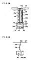
- an equivalent circuit of the dielectric coaxial resonator 28 and surrounding thereof is formed as shown in Fig. 2B.
- These dielectric coaxial resonator 28 and capacitor 44 are selected so that the series resonance frequencies thereof are located in the band of 845 - 846.5 MHz to be attenuated.
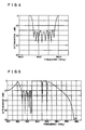
- this band-stop filter 18 the eight-stage dielectric coaxial resonator 28, the amplifier circuit 40 and the like are connected by the above-described coaxial cable 46. Furthermore, the both ends of that coaxial cable 46 are connected to the input end 18a and the output end 18b which penetrate through one side wall of the case 24, respectively. Accordingly, an equivalent circuit of this band-stop filter 18 is formed as shoen in Fig. 3. Also, this band-stop filter 18 has a frequency characteristic as shown in Fig. 4.
- the conductor pattern 42 of each substrate 30 is connected to a power source end 18c penetrating through the other side wall of the case 24. Then, to this power source end 18c, a DC power source 48 in the case 12 is connected, and power is supplied from the DC power source 48.
- the intermediate-stages band-stop filter 20 has a structure similar to the above-described band-stop filter 18, but differs therefrom in that it has 10-stage dielectric coaxial resonator and the like and in that the attenuation band is the band of 849 MHz and higher.
- the last-stage band-stop filter 22 differs from the above-described band-stop filter 18 in that it has the 18-stage dielecteic coaxial resonator and the like and in that the attenuation band is the band of 835 MHz and lower.
- the output end of the last-stage band-stop filter 22 is connected to a coaxial connector 50 as an output end penetrating through the side wall of the case 12.
- the band-pass filter 16 transmits a signal of the band containing the desired frequency bands, and the post-stage band-stop filters 18, 20 and 22 sharply attenuate signals of the undesirable frequency bands among signals transmitted by the band-pass filter 16, that is, signals of the band of 845 - 846.5 MHz, the band of 849 MHz and higher and the band of 835 MHz and lower, respectively. Accordingly, this filter apparatus 10 has a frequency characteristic as shown in Fig. 5.
- the dielectric coaxial resonator of ⁇ /4 is used in the band-stop filter, but the dielectric coaxial resonator of ⁇ /2 may be used in place of ⁇ /4.
- one end side of the inner conductor 28b of the dielectric coaxial resonator 28 of ⁇ /2 is coupled to the amplifier 40 as an active circuit, and further, for example, a metal cylindrical body 43 is fixed to the other end side of the inner conductor 28b with a conductive adhesive, and the both ends of the capacitor 44 are soldered to the metal cylindrical body 43 and the coaxial cable 46 as a transmission line.
- a resonator having another structure such as the strip-line resonator may be used without being limited to the dielectric coaxial resonator, and the resonator mode threof may be a mode such as the TE mode or the TM mode.
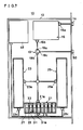
- Fig. 7 is an illustration view showing another embodiment of the present invention. This embodiment differs from the embodiment as shown in Fig. 1 particularly in the construction of the post-stage of the first ban-pass filter 16.
- the output end 16b of the first band-pass filter 16 is connected to a first terminal 19a of a circulator 19 as a non-reversible cercuit element.
- input ends 21a, 23a and 25a of three second band-pass filters 21, 23 and 25 are connected in common to a second terminal 19b which becomes the output side when the terminal 19a of this circulator 19 is set as the input side.
- These second band-pass filters 21, 23 and 25 have pass bands in bands wanted to be attenuated among bands transmitted by the band-pass filter 16, for example, a band of 845 - 846.5 MHz, a band of 849 MHz and higher and a band of 835 MHz and lower, respectively.
- These second band-pass filters 21, 23 and 25 differ in the number of stages of the dielectric coaxial resonator to be used or the like and the pass band, but have structures similar to one another, and therefore detailed description is made particularly on one of the second band-pass filters 21.
- this second band-pass filter 21 comprises eight sets of a dielectric coaxial resonator 31 of ⁇ /4 whose outer conductor 31a is grounded and a substrate 33 having an amplifier circuit 45 as an active circuit whlich is coupled to the dielectric coaxial resonator 31.
- this second band-pass filter 21 cosmprises, for example, a cuboid-shaped case 27 composed of metal, and space in this case 27 is divided into eight housing parts by seven partition plates 29 composed of metal. Then, in each of these housing parts, for example, the dielectric coaxial resonator 31 of ⁇ /4 and the substrate 33 composed of an insulating material such as epoxy resin are housed. In this case, the outer conductor 31a as one end of each dielectric coaxial resonator 31 is grounded to the case 27. Also, each substrate 33 is disposed at the open end side of the dielectric coaxial resonator 31.
- an L-shaped conductor pattern 35 is formed, and to one end of this conductor pattern 35, and inner conductor 31b as the other end of the dielectric coaxial resonator 31 is connected, for example, by a conductor ribbon 37.
- two electrodes 39a and 39b are formed in the vicinity of one end of the conductor pattern 35, and these electrodes 39a and 39b are coupled to the conductor pattern 35 respectively through gap capacities produced by gaps 41a and 41b.
- the amplifier circuit 45 as an active circuit which is configurated, for example, with a Si bipolar transistor is connected by lines 43a and 43b for phase adjustment.
- this amplifier circuit 45 is coupled to the dielectric coaxial resonator 31. Also, this amplifier circuit 45 is configurated so as to become a negative resistance in the operation band of the second band-pass filter 21. For this reason, the apparent value of Q of the second band-pass filter 21 becomes large in the operation band of the second band-pass filter 21. Furthermore, on the substrate 33, a conductor pattern 47 for supplying power to this amplifier circuit 45 is formed.
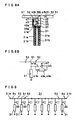
- each electrode 51 is connected to each electrode 51 as a transmission line by each conductor ribbon 49. Also, these electrodes 51 are disposed in a line with intervals kept so that gap capacities are produced by gaps 52 between them. Accordingly, an equivalent cercuit of this dielectric coaxial resonator 31 and surrounding thereof is formed as shown in Fig. 8B.
- this second band-pass filter 21 is expressed by an equivalent circuit as shown in Fig. 9.
- the output end 21b of this second band-pass filter 21 is put in no-load state in this embodiment.
- a load for example, a resistance may be connected to the output end 21b of this second band-pass filter 21.
- the dielectric coaxial resonator 31 and the gap capacities such as the one between the electrodes 51 in the second band-pass filter 21 are selected so that the resonance frequencies thereof are located in the band of 845 - 846.5 MHz to be attenuated. Accordingly, for this second band-pass filter 21, the frequency characteristic of reflection at the input end 21a side becomes as shown in Fig. 10.
- each substrate 33 is connected to a power source end 21c penetrating through the side wall of the case 27. Then, to this power source end 21c, the DC power source 48 in the case 12 is connected, and power is supplied from the DC power source 48.
- Another second band-pass filter 23 has a structure similar to the above-described band-pass filter 21, but differs therefrom in that this has a 10-stage dielectric coaxial resonator and the like and the pass band is the band of 849 MHz and higher.
- Still another second band-pass filter 25 differs from the above-described band-pass filter 21 in that this has a 18-stage dielectric coaxial resonator and the like, and the pass band is the band of 835 MHz and lower.
- each second band-pass filter is configurated so as to become a negative resistance in the operaion band of the second band-pass filter.
- a third terminal 19c becoming the output side when the second terminal 19b of the circulator 19 is set as the input side is connected to the coaxial connector 50 as the output terminal penetrating through the side wall of the case 12.
- the first band-pass filter 16 transmits a signal of the band containing the desired frequency bands to the first end 19a of the circulator 19. Then, this circulator 19 gives the signal to the input ends 21a, 23a and 25a of three second band-pass filters 21, 23 and 25.
- One second band-pass filter 21 has the pass band in the frequency band of 845 - 846.5 MHz to be attenuated, and therefore sharply reflects signals of bands other than this band, giving them to the second terminal 19b of the circulator 19.
- the other second band-pass filter 23 sharply reflects signals of bands other than the band of 849 MHz and hegher, and gives them to the second terminal 19b of the circulator 19
- the still other second band-pass filter 25 sharply reflects signals of bands other than the band of 835 MHz and lower, giving them to the second terminal 19b of the circulator 19. Accordingly, the signal of the desired frequency bands is given to the second terminal 19b of the circulator 19.
- the signal of the desired frequency bands is outputted from the third terminal 19c of the cerculator 19, and the signal is given to the coaxial connector 50 as the output terminal. Accordingly, in this filter apparatus 10, a frequency characteristic as shown in Fig. 11 is obtained.
- the first band-pass filter 16 is installed in the pre-stage of the circulator 19, but in the present invention, it is also possible that no filter is installed in the pre-stage of the circulator 19. In this case, the first terminal 19a of the circulator 19 is connected directly to the coaxial connector 14 as the input terminal.
- the dielectric coaxial resonator of ⁇ /4 is used in the second band-pass filter, but the dielectric coaxial resonator of ⁇ /2 may be used in place of ⁇ /4.
- one end side of the inner conductor 31b of the dielectric coaxial resonator 31 of ⁇ /2 is coupled to the amplifier circuit 45 as an active circuit, and the other end side thereof is connected to the electrode 50 as a transmission line.
- a resonator having another structure such as the strip-line resonator may be used without being limited to the dielectric coaxial resonator, and the resonance mode thereof may be a mode such as the TE mode or the TM mode.
- the embodiment as shown in Fig. 7 has a characteristic of attenuating a plurality of bands, but the present invention is applicable also to a filter apparatus having a characteristic of attenuating one band.
- the present invention is applicable also to a filter apparatus having a characteristic of attenuating one band.
- only the input end of one second band-pass filter having the pass band in the band to be attenuated has only to be connected to the second terminal 19b of the circulator 19.
- an active circuit is coupled to only any one of the resonators.
- the active circuit is desirably coupled only to the pre-stage or post-stage resonator, and in view of noise generated on the circulator side from the second band-pass filter, it is most desirable to couple the active circuit to the post-stage resonator.
- each of the embodiments as shoen in Fig. 1 and Fig. 7 has a characteristic of transmitting two different bands, but in the present invention, a filter apparatus having a characteristic of transitting three or more different bands may be configurated.
- a filter apparatus having a characteristic of transitting three or more different bands may be configurated.
- three or more band-stop filter having attenuation bands differing from one another have only to be installed in the post-stage of the band-pass filter, or, in the embodiment as shown in Fig. 7, three or more second band-pass filters having pass bands differing from one another have only to be connected to the circulator.
Landscapes
- Physics & Mathematics (AREA)
- Electromagnetism (AREA)
- Control Of Motors That Do Not Use Commutators (AREA)
- Filters And Equalizers (AREA)
Applications Claiming Priority (4)
| Application Number | Priority Date | Filing Date | Title |
|---|---|---|---|
| JP1150998A JPH0750841B2 (ja) | 1989-06-13 | 1989-06-13 | マルチバンド用フィルタ |
| JP150998/89 | 1989-06-13 | ||
| JP219882/89 | 1989-08-25 | ||
| JP1219882A JP2720209B2 (ja) | 1989-08-25 | 1989-08-25 | 帯域阻止形フィルタ |
Publications (3)
| Publication Number | Publication Date |
|---|---|
| EP0402873A2 true EP0402873A2 (de) | 1990-12-19 |
| EP0402873A3 EP0402873A3 (de) | 1991-07-03 |
| EP0402873B1 EP0402873B1 (de) | 1996-08-28 |
Family
ID=26480401
Family Applications (1)
| Application Number | Title | Priority Date | Filing Date |
|---|---|---|---|
| EP90111126A Expired - Lifetime EP0402873B1 (de) | 1989-06-13 | 1990-06-12 | Filtergerät |
Country Status (3)
| Country | Link |
|---|---|
| US (2) | US5132651A (de) |
| EP (1) | EP0402873B1 (de) |
| DE (1) | DE69028249T2 (de) |
Cited By (2)
| Publication number | Priority date | Publication date | Assignee | Title |
|---|---|---|---|---|
| GB2257308A (en) * | 1991-05-20 | 1993-01-06 | American Telephone & Telegraph | Folded interdigital notch filter. |
| WO2022048932A1 (en) * | 2020-09-03 | 2022-03-10 | Novelda As | Filter |
Families Citing this family (10)
| Publication number | Priority date | Publication date | Assignee | Title |
|---|---|---|---|---|
| US5132651A (en) * | 1989-06-13 | 1992-07-21 | Murata Manufacturing Co., Ltd. | Filter apparatus |
| US5684439A (en) * | 1995-10-10 | 1997-11-04 | Motorola, Inc. | Half wave ceramic filter with open circuit at both ends |
| US5721521A (en) * | 1996-08-05 | 1998-02-24 | Lucent Technologies Inc. | Notch-enhancement in band-reject filters |
| EP1686644B1 (de) | 1997-01-07 | 2009-03-04 | Panasonic Corporation | Mehrschichtiges Filter |
| US5864265A (en) * | 1997-06-30 | 1999-01-26 | Motorola Inc. | Bandstop filter module with shunt zero |
| US6326854B1 (en) * | 1999-09-30 | 2001-12-04 | Nortel Networks Limited | Coaxial resonator and oscillation circuits featuring coaxial resonators |
| SE0102151D0 (sv) * | 2001-06-18 | 2001-06-18 | Ericsson Telefon Ab L M | Active filter |
| US20050122190A1 (en) * | 2003-12-04 | 2005-06-09 | Chu Peter F. | VHF band pass filter built with ceramic coaxial resonator |
| KR101266945B1 (ko) * | 2012-02-06 | 2013-05-30 | 주식회사 이너트론 | 다중 대역 통과 필터 |
| EP2733781A1 (de) | 2012-11-16 | 2014-05-21 | Alcatel-Lucent | Filteranordnung und Filterungsverfahren |
Family Cites Families (15)
| Publication number | Priority date | Publication date | Assignee | Title |
|---|---|---|---|---|
| US2297451A (en) * | 1938-12-29 | 1942-09-29 | Bendel Hermann | Method of selective filtering of frequency band ranges |
| US2994844A (en) * | 1958-10-15 | 1961-08-01 | Motorola Inc | Filter construction |
| FR1355627A (fr) * | 1963-01-31 | 1964-03-20 | Comp Generale Electricite | Réseau déphaseur d'ondes électriques à affaiblissement réduit |
| US4159454A (en) * | 1977-12-30 | 1979-06-26 | The United States Of America As Represented By The Secretary Of The Air Force | Plug-in filter network for separating a communication frequency into discrete frequency channels |
| US4292607A (en) * | 1980-03-19 | 1981-09-29 | Westinghouse Electric Corp. | Broadband circuit for microwave S/N enhancers |
| US4553264A (en) * | 1982-09-17 | 1985-11-12 | Matsushita Electric Industrial Co., Ltd. | Double superheterodyne tuner |
| US4538123A (en) * | 1984-01-20 | 1985-08-27 | The United States Of America As Represented By The Secretary Of The Army | Dielectric waveguide bandpass apparatus |
| US4816788A (en) * | 1986-07-01 | 1989-03-28 | Murata Manufacturing Co., Ltd. | High frequency band-pass filter |
| JPS63110801A (ja) * | 1986-10-28 | 1988-05-16 | Murata Mfg Co Ltd | アクテイブフイルタ |
| JPH063841B2 (ja) * | 1986-12-04 | 1994-01-12 | 株式会社村田製作所 | 高周波フイルタ |
| JPS63157502A (ja) * | 1986-12-20 | 1988-06-30 | Murata Mfg Co Ltd | 伝送回路 |
| JPS63157501A (ja) * | 1986-12-20 | 1988-06-30 | Murata Mfg Co Ltd | アクテイブトラツプフイルタ |
| JPH01227530A (ja) * | 1988-03-07 | 1989-09-11 | Kokusai Electric Co Ltd | 分波器 |
| US4823098A (en) * | 1988-06-14 | 1989-04-18 | Motorola, Inc. | Monolithic ceramic filter with bandstop function |
| US5132651A (en) * | 1989-06-13 | 1992-07-21 | Murata Manufacturing Co., Ltd. | Filter apparatus |
-
1990
- 1990-06-11 US US07/536,175 patent/US5132651A/en not_active Expired - Lifetime
- 1990-06-12 EP EP90111126A patent/EP0402873B1/de not_active Expired - Lifetime
- 1990-06-12 DE DE69028249T patent/DE69028249T2/de not_active Expired - Lifetime
-
1992
- 1992-03-06 US US07/846,822 patent/US5291160A/en not_active Expired - Lifetime
Cited By (4)
| Publication number | Priority date | Publication date | Assignee | Title |
|---|---|---|---|---|
| GB2257308A (en) * | 1991-05-20 | 1993-01-06 | American Telephone & Telegraph | Folded interdigital notch filter. |
| GB2257308B (en) * | 1991-05-20 | 1995-04-26 | American Telephone & Telegraph | Folded interdigital notch filter |
| WO2022048932A1 (en) * | 2020-09-03 | 2022-03-10 | Novelda As | Filter |
| US12451868B2 (en) | 2020-09-03 | 2025-10-21 | Novelda As | Filter |
Also Published As
| Publication number | Publication date |
|---|---|
| US5291160A (en) | 1994-03-01 |
| EP0402873B1 (de) | 1996-08-28 |
| DE69028249T2 (de) | 1997-02-20 |
| EP0402873A3 (de) | 1991-07-03 |
| US5132651A (en) | 1992-07-21 |
| DE69028249D1 (de) | 1996-10-02 |
Similar Documents
| Publication | Publication Date | Title |
|---|---|---|
| US5467065A (en) | Filter having resonators coupled by a saw filter and a duplex filter formed therefrom | |
| CN100382384C (zh) | 带定向耦合器的低通滤波器和蜂窝电话 | |
| KR100418607B1 (ko) | 대역필터, 듀플렉서, 고주파 모듈 및 통신장치 | |
| US5812036A (en) | Dielectric filter having intrinsic inter-resonator coupling | |
| EP0788179A2 (de) | Dielektrisches Filter | |
| US6326863B1 (en) | Matching circuit chip, filter with matching circuit, duplexer and cellular phone | |
| EP0575174A1 (de) | Verbund-Duplexfilter | |
| JPS6150523B2 (de) | ||
| EP0402873A2 (de) | Filtergerät | |
| EP0085180B1 (de) | Miniaturisierter Antennenduplexer mit SAW-Filter | |
| US4449108A (en) | Band-stop filter for VHF-UHF band | |
| US4799033A (en) | Microwave separator | |
| JPH11186819A (ja) | 帯域阻止フィルタ及びデュプレクサ | |
| KR20010033575A (ko) | 캐스케이드 필터와 중간 증폭기부를 갖는 rf 수신기 | |
| JPH0234001A (ja) | 帯域阻止フイルタ | |
| US4313097A (en) | Image frequency reflection mode filter for use in a high-frequency receiver | |
| EP0190902A2 (de) | Mischschaltung | |
| JP3353717B2 (ja) | 誘電体フィルタ、誘電体デュプレクサおよび通信機装置 | |
| US6507250B1 (en) | Dielectric filter, dielectric duplexer, and communication equipment | |
| JPH0750841B2 (ja) | マルチバンド用フィルタ | |
| US6177851B1 (en) | High-frequency electronic device | |
| JPH04196829A (ja) | 分波装置およびそれを用いた移動無線機 | |
| JP2720209B2 (ja) | 帯域阻止形フィルタ | |
| KR200167764Y1 (ko) | 듀플렉서 | |
| JPH0134483B2 (de) |
Legal Events
| Date | Code | Title | Description |
|---|---|---|---|
| PUAI | Public reference made under article 153(3) epc to a published international application that has entered the european phase |
Free format text: ORIGINAL CODE: 0009012 |
|
| AK | Designated contracting states |
Kind code of ref document: A2 Designated state(s): DE GB SE |
|
| 17P | Request for examination filed |
Effective date: 19901220 |
|
| PUAL | Search report despatched |
Free format text: ORIGINAL CODE: 0009013 |
|
| AK | Designated contracting states |
Kind code of ref document: A3 Designated state(s): DE GB SE |
|
| 17Q | First examination report despatched |
Effective date: 19940218 |
|
| GRAH | Despatch of communication of intention to grant a patent |
Free format text: ORIGINAL CODE: EPIDOS IGRA |
|
| GRAA | (expected) grant |
Free format text: ORIGINAL CODE: 0009210 |
|
| AK | Designated contracting states |
Kind code of ref document: B1 Designated state(s): DE GB SE |
|
| REF | Corresponds to: |
Ref document number: 69028249 Country of ref document: DE Date of ref document: 19961002 |
|
| PLBE | No opposition filed within time limit |
Free format text: ORIGINAL CODE: 0009261 |
|
| STAA | Information on the status of an ep patent application or granted ep patent |
Free format text: STATUS: NO OPPOSITION FILED WITHIN TIME LIMIT |
|
| 26N | No opposition filed | ||
| REG | Reference to a national code |
Ref country code: GB Ref legal event code: IF02 |
|
| PGFP | Annual fee paid to national office [announced via postgrant information from national office to epo] |
Ref country code: SE Payment date: 20090605 Year of fee payment: 20 |
|
| PGFP | Annual fee paid to national office [announced via postgrant information from national office to epo] |
Ref country code: DE Payment date: 20090604 Year of fee payment: 20 Ref country code: GB Payment date: 20090610 Year of fee payment: 20 |
|
| REG | Reference to a national code |
Ref country code: GB Ref legal event code: PE20 Expiry date: 20100611 |
|
| EUG | Se: european patent has lapsed | ||
| PG25 | Lapsed in a contracting state [announced via postgrant information from national office to epo] |
Ref country code: GB Free format text: LAPSE BECAUSE OF EXPIRATION OF PROTECTION Effective date: 20100611 |
|
| PG25 | Lapsed in a contracting state [announced via postgrant information from national office to epo] |
Ref country code: DE Free format text: LAPSE BECAUSE OF EXPIRATION OF PROTECTION Effective date: 20100612 |