EP0400324A2 - Semiconductor package - Google Patents
Semiconductor package Download PDFInfo
- Publication number
- EP0400324A2 EP0400324A2 EP90107745A EP90107745A EP0400324A2 EP 0400324 A2 EP0400324 A2 EP 0400324A2 EP 90107745 A EP90107745 A EP 90107745A EP 90107745 A EP90107745 A EP 90107745A EP 0400324 A2 EP0400324 A2 EP 0400324A2
- Authority
- EP
- European Patent Office
- Prior art keywords
- lead frame
- conductors
- chip
- terminals
- wires
- Prior art date
- Legal status (The legal status is an assumption and is not a legal conclusion. Google has not performed a legal analysis and makes no representation as to the accuracy of the status listed.)
- Withdrawn
Links
Images


Classifications
-
- H—ELECTRICITY
- H10—SEMICONDUCTOR DEVICES; ELECTRIC SOLID-STATE DEVICES NOT OTHERWISE PROVIDED FOR
- H10W—GENERIC PACKAGES, INTERCONNECTIONS, CONNECTORS OR OTHER CONSTRUCTIONAL DETAILS OF DEVICES COVERED BY CLASS H10
- H10W70/00—Package substrates; Interposers; Redistribution layers [RDL]
- H10W70/40—Leadframes
-
- H—ELECTRICITY
- H10—SEMICONDUCTOR DEVICES; ELECTRIC SOLID-STATE DEVICES NOT OTHERWISE PROVIDED FOR
- H10W—GENERIC PACKAGES, INTERCONNECTIONS, CONNECTORS OR OTHER CONSTRUCTIONAL DETAILS OF DEVICES COVERED BY CLASS H10
- H10W72/00—Interconnections or connectors in packages
- H10W72/50—Bond wires
-
- H—ELECTRICITY
- H10—SEMICONDUCTOR DEVICES; ELECTRIC SOLID-STATE DEVICES NOT OTHERWISE PROVIDED FOR
- H10W—GENERIC PACKAGES, INTERCONNECTIONS, CONNECTORS OR OTHER CONSTRUCTIONAL DETAILS OF DEVICES COVERED BY CLASS H10
- H10W72/00—Interconnections or connectors in packages
- H10W72/50—Bond wires
- H10W72/551—Materials of bond wires
- H10W72/552—Materials of bond wires comprising metals or metalloids, e.g. silver
- H10W72/5522—Materials of bond wires comprising metals or metalloids, e.g. silver comprising gold [Au]
-
- H—ELECTRICITY
- H10—SEMICONDUCTOR DEVICES; ELECTRIC SOLID-STATE DEVICES NOT OTHERWISE PROVIDED FOR
- H10W—GENERIC PACKAGES, INTERCONNECTIONS, CONNECTORS OR OTHER CONSTRUCTIONAL DETAILS OF DEVICES COVERED BY CLASS H10
- H10W74/00—Encapsulations, e.g. protective coatings
-
- H—ELECTRICITY
- H10—SEMICONDUCTOR DEVICES; ELECTRIC SOLID-STATE DEVICES NOT OTHERWISE PROVIDED FOR
- H10W—GENERIC PACKAGES, INTERCONNECTIONS, CONNECTORS OR OTHER CONSTRUCTIONAL DETAILS OF DEVICES COVERED BY CLASS H10
- H10W90/00—Package configurations
- H10W90/701—Package configurations characterised by the relative positions of pads or connectors relative to package parts
- H10W90/751—Package configurations characterised by the relative positions of pads or connectors relative to package parts of bond wires
- H10W90/756—Package configurations characterised by the relative positions of pads or connectors relative to package parts of bond wires between a chip and a stacked lead frame, conducting package substrate or heat sink
Definitions
- This invention relates to packaged wire bonded semiconductor chips. More particularly, it relates to a wire bonded chip in which none of the wires used to make electrical contact between the lead frame and the chip terminals cross one another, thus eliminating a possible defect mechanism.
- Wire bonding techniques have long been employed to position and affix leads to semiconductor chips prior to encapsulation of the chip in a protective coating.
- Such techniques generally employ a lead frame to which the semiconductor chip is attached prior to encapsulation.
- Gold wires are used to connect terminals on the surface of the semiconductor chip to corresponding lead frame conductors.
- the initial design is such that these wires are kept within specified lengths. Good practice dictates that the length of the wires should be minimized and not exceed 100 times the diameter of the wire.
- the new designs often require one or more new terminal locations while the outside circuit or machine requirements demand that the external lead frame conductors remain in the same position. In such a case, extremely long wires which can cross several such other wires might be considered. If such long wires are used, as these long wires pass from the conductors of the lead frame to the respective terminal on the chip surface, undesirable effects can occur especially during the subsequent encapsulation step.
- Another object of the invention is to provide a semiconductor chip package in which lead frame conductors can be easily and safely connected to a number of different chip terminals, thereby permitting the use of the same external lead frame configuration with different semiconductor chips.
- an encapsulated semiconductor module in which a semiconductor chip, having a major surface with terminals thereon, is deposed within the encapsulating material, a plurality of self-supporting, unitary, discrete, and continuous lead frame conductors formed of metal sheet stock are positioned at various locations around the chip and cantilevered out of the encapsulating material, so that discrete wires can be used to connect respective ones of said conductors to respective ones of said terminals.
- excessively long bonding wires are avoided by connecting a selected one of said lead frame conductors to a parallel conductor by a jumper wire and connecting the parallel conductor to the desired terminal with a short wire.
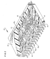
- a semiconductor package 12 containing a semiconductor chip 14 in which part of the encapsulation is removed is shown in Fig. 1.
- the chip 14 supports a multiconductor lead frame 15 whose leads or conductors 18 are electrically connected to respective terminals 17 on the surface of the semiconductor chip 14 by bonding wires 16.
- the conductors 18 are supported as a unit by the lead frame bar 20 shown in phantom in Fig. 1. After the encapsulation material is hardened, this lead frame bar 20 is removed.
- lead frame has a definite meaning in the semiconductor art.
- the material, thickness, strength, etc. of such lead frames has long been specified and known to the art, such that the use of the term “lead frame” is all that is necessary to purchase such items.
- the term “lead frame” means a metal structure, preferably a spot plated copper alloy, formed from sheet stock and a sufficient size and strength to meet specific mechanical strength requirements. For example, such a lead frame is discussed in the Semiconductor International , April, 1985.
- the lead frame is typically between 127 ⁇ m (0.005) and 381 ⁇ m (0.015 inches) thick and comprised of a number of fingers or conductors between 203 ⁇ m (0.008) and 431.8 ⁇ m (0.017 inches) wide. These conductors are thus of a sufficient mechanical strength to be successfully handled and inserted into sockets or assembled and soldered to printed circuit boards.
- the interior portions of the lead frame conductors 18 extend over the semiconductor chip 14 but are separated from the semiconductor chip surface by an interposer 22 that can also serve both as an insulator and/or as an alpha particle barrier.
- this interposer 22 should be comprised of a polymeric film having thermal stability at temperatures of 175°C and not contain an ionizable species such as halides and active metals, including sodium, potassium, and phosphorus.
- Polyimide films are suitable for such use as alpha barriers.
- One such polyimide film is sold under the trade name Kapton.
- Kapton films should be between 25.4 ⁇ m (1.0) and 50.8 um (2.0 mils) in thickness and may be thermally enhanced by alumina or silicon nitride.
- the interposer layer 22 can also be solely an adhesive layer, so long as it is electrically insulating.
- an adhesive layer is applied to the lead frame conductors or the top active surface of chip 14; i.e., the major upper surface of the chip which contains the chip terminals 17.
- a dielectric interposer positioned between the lead frame conductors and the chip.
- Adhesives which are suitable for use for attaching the lead frame conductors to the semiconductor chip or to such a dielectric interposer can be selected from the group of epoxies, acrylics, and polyimides containing phenolics, such as polyimide-butyral:phenolic.
- wires 16 are bonded to the tips of selected lead frame conductors 18 and bonded to selected chip terminals 17. Each wire extends from the tip of a selected lead frame conductor to a selected chip terminal.
- the device is encapsulated in a suitable plastic material using well known packaging techniques.
- the lead frame bar 20 which supports the leads and which is required during encapsulation, is removed. This lead frame bar is originally provided to connect the conductors 18, of the lead frame 15, so as to impart rigidity to the lead frame 15 and to limit flow of the encapsulating material. Because the lead frame bar 20 has been removed, it is shown in the figure in phantom.
- those portions of the lead frame conductors 18, which extend beyond the encapsulation 19, may be formed as required.
- respective terminals 17 are connected to respective conductors 18 by wires 16.
- the configuration of the lead frame conductors 18 is preferably such that the length of the wires 17 is maintained at a length of less than about 2.032 mm (80 mils). Minimizing the length of these wires 17 not only improves the electrical performance of the packaged semiconductor chip, but further imparts a greater rigidity to the wires reducing the possibility of breakage or shorting of the wires to other elements in the package.
- the initial semiconductor chip design and lead frame design is usually done so as to assure such wires are as short as possible and within the 2.032 mm (80 mil) length.
- the wires 16 are maintained in this short configuration by arranging the bulk of the terminal pads 17 in a central row. This arrangement not only reduces the impedance of the chip itself by reducing conducting channel lengths within the chip, but also reduces time delays, signal noise, and etc.
- lead frame conductor 18a is bonded via wire 16a to a nearby terminal 17a.
- the terminal 17a will have to be eliminated and functionally relocated because of a chip redesign.
- FIG. 2 shows for example, the prior art method of accommodating this design change.
- Fig. 2 there is shown the same structure as shown in Fig. 1 except that the terminal 17a has been eliminated and the conductor 18a is now connected to a distant, newly created terminal 17d via an excessively long wire 24, which crosses the wire 16b, connected between conductor 18b and pad 17b, and wire 16c connected between conductor 18c and pad 17c.
- any distortion of this wire 24, during encapsulation, can cause the wire 24 to bend or deform such that it can contact and short out either or both of the crossed wires 16a or 16b, thus causing a failure in the packaged chip. It is desirable that this is avoided.
- Fig. 3 shows the present invention in which this long wire 24 has been completely eliminated and with its elimination, the defect mechanisms described above.
- parallel conductors 18a and 18d are each provided with a respective T-like extension or jutty, 30 and 31. These jutties 30 and 31 extend toward one another and toward an intermediate conductor 18b.
- a distinctive short jumper wire 32 spans conductor 18b and connects the two jutties 30 and 31 while a separate and distinct short wire 33 connects lead 18d to the newly created chip terminal 17d.
- the end of conductor 18d can be excised during removal of the cross member 20 after encapsulation.
- each such extended jutty need only be of a size to accommodate the bonding of a wire thereto and need not extend any significant distance toward any other jutty. Also, such jutties can be placed at any convenient place on the lead frame conductor.
Landscapes
- Lead Frames For Integrated Circuits (AREA)
- Wire Bonding (AREA)
Abstract
In an encapsulated semiconductor module (12) in which a semiconductor chip (14), having a major surface with terminals thereon, is deposed within the encapsulating material (19), a plurality of self-supporting, unitary, discrete, and continuous lead frame conductors (18) formed of metal sheet stock are positioned at various locations around the chip and cantilevered out of the encapsulating material, so that discrete wires (16) can be used to connect respective ones of said conductors to respective ones of said terminals. In the present invention excessively long bonding wires are avoided by connecting a selected one of said lead frame conductors to a parallel conductor by a jumper wire and connecting the parallel conductor to the desired terminal with a short wire.
Description
- This invention relates to packaged wire bonded semiconductor chips. More particularly, it relates to a wire bonded chip in which none of the wires used to make electrical contact between the lead frame and the chip terminals cross one another, thus eliminating a possible defect mechanism.
- Wire bonding techniques have long been employed to position and affix leads to semiconductor chips prior to encapsulation of the chip in a protective coating.
- Such techniques generally employ a lead frame to which the semiconductor chip is attached prior to encapsulation. Gold wires are used to connect terminals on the surface of the semiconductor chip to corresponding lead frame conductors.
- In general, the initial design is such that these wires are kept within specified lengths. Good practice dictates that the length of the wires should be minimized and not exceed 100 times the diameter of the wire. However, when new chip designs are created in order, for example, to stack the chips in a denser package or to replace prior existing chips, the new designs often require one or more new terminal locations while the outside circuit or machine requirements demand that the external lead frame conductors remain in the same position. In such a case, extremely long wires which can cross several such other wires might be considered. If such long wires are used, as these long wires pass from the conductors of the lead frame to the respective terminal on the chip surface, undesirable effects can occur especially during the subsequent encapsulation step. For example, during the encapsulation steps there exists a strong likelihood that any such long wire will deform and short to one or more of the wires it is crossing. The possibility of such shorting, during the encapsulation process, increases with both the length of the crossing wire and the number of wires over which it crosses.
- It is the object of this invention to provide a packaged semiconductor chip with improved mechanical, and electrical performance.
- Another object of the invention is to provide a semiconductor chip package in which lead frame conductors can be easily and safely connected to a number of different chip terminals, thereby permitting the use of the same external lead frame configuration with different semiconductor chips.
- It is yet another object of the present invention to provide a semiconductor package with enhanced reliability.
- These and other objects of the present invention as claimed provided in an encapsulated semiconductor module in which a semiconductor chip, having a major surface with terminals thereon, is deposed within the encapsulating material, a plurality of self-supporting, unitary, discrete, and continuous lead frame conductors formed of metal sheet stock are positioned at various locations around the chip and cantilevered out of the encapsulating material, so that discrete wires can be used to connect respective ones of said conductors to respective ones of said terminals. In the present invention excessively long bonding wires are avoided by connecting a selected one of said lead frame conductors to a parallel conductor by a jumper wire and connecting the parallel conductor to the desired terminal with a short wire.
- These and other objects, features, and advantages of the invention will be apparent from the following more particular description of the preferred embodiment of the invention as illustrated in the accompanying drawings, in which:
- Fig. 1 is a schematic representation of a wire bonded encapsulated semiconductor chip. Part of the encapsulation material has been broken away to expose the lead frame conductors, the semiconductor chip, the chip terminals, and the wires used to connect the conductors to the chip terminals;
- Fig. 2 shows the chip in Fig. 1 with one long wire that has been rerouted because of design changes in the terminal locations on the chip surface; and
- Fig. 3 shows the redesigned chip of Fig. 2 in which one embodiment of the present invention is used to avoid the hazards of the long wire shown in Fig. 2.
- A
semiconductor package 12 containing asemiconductor chip 14 in which part of the encapsulation is removed is shown in Fig. 1. Thechip 14 supports amulticonductor lead frame 15 whose leads orconductors 18 are electrically connected to respective terminals 17 on the surface of thesemiconductor chip 14 bybonding wires 16. - During encapsulation in
material 19, theconductors 18 are supported as a unit by thelead frame bar 20 shown in phantom in Fig. 1. After the encapsulation material is hardened, thislead frame bar 20 is removed. - The term "lead frame", as used herein, has a definite meaning in the semiconductor art. The material, thickness, strength, etc. of such lead frames has long been specified and known to the art, such that the use of the term "lead frame" is all that is necessary to purchase such items. In essence, the term "lead frame", means a metal structure, preferably a spot plated copper alloy, formed from sheet stock and a sufficient size and strength to meet specific mechanical strength requirements. For example, such a lead frame is discussed in the Semiconductor International, April, 1985. In the present invention the lead frame is typically between 127 µm (0.005) and 381 µm (0.015 inches) thick and comprised of a number of fingers or conductors between 203 µm (0.008) and 431.8 µm (0.017 inches) wide. These conductors are thus of a sufficient mechanical strength to be successfully handled and inserted into sockets or assembled and soldered to printed circuit boards.
- As shown in Fig. 1, the interior portions of the
lead frame conductors 18 extend over thesemiconductor chip 14 but are separated from the semiconductor chip surface by aninterposer 22 that can also serve both as an insulator and/or as an alpha particle barrier. - When it is desired that this
interposer 22 be also an alpha particle barrier, then it should be comprised of a polymeric film having thermal stability at temperatures of 175°C and not contain an ionizable species such as halides and active metals, including sodium, potassium, and phosphorus. Polyimide films are suitable for such use as alpha barriers. One such polyimide film is sold under the trade name Kapton. Desirably, such Kapton films should be between 25.4 µm (1.0) and 50.8 um (2.0 mils) in thickness and may be thermally enhanced by alumina or silicon nitride. - The
interposer layer 22 can also be solely an adhesive layer, so long as it is electrically insulating. In use, such an adhesive layer is applied to the lead frame conductors or the top active surface ofchip 14; i.e., the major upper surface of the chip which contains the chip terminals 17. To absolutely assure there is no possibility of short circuit to the chip, in spite of the fact that the chips are coated with this passivating insulating adhesive, it is preferable to further use a dielectric interposer positioned between the lead frame conductors and the chip. When such an interposer is used, the adhesive layer should be applied to both surfaces of the interposer with suitable adhesive materials. Adhesives which are suitable for use for attaching the lead frame conductors to the semiconductor chip or to such a dielectric interposer can be selected from the group of epoxies, acrylics, and polyimides containing phenolics, such as polyimide-butyral:phenolic. - Once the
lead frame 15 has been suitably secured to the surface of the chip,wires 16 are bonded to the tips of selectedlead frame conductors 18 and bonded to selected chip terminals 17. Each wire extends from the tip of a selected lead frame conductor to a selected chip terminal. Once the desired wire bonds are in place, as shown in Figure 1, the device is encapsulated in a suitable plastic material using well known packaging techniques. Following encapsulation of the assembly, thelead frame bar 20, which supports the leads and which is required during encapsulation, is removed. This lead frame bar is originally provided to connect theconductors 18, of thelead frame 15, so as to impart rigidity to thelead frame 15 and to limit flow of the encapsulating material. Because thelead frame bar 20 has been removed, it is shown in the figure in phantom. - Following this removal of the
lead frame bar 20, those portions of thelead frame conductors 18, which extend beyond theencapsulation 19, may be formed as required. - As previously noted, respective terminals 17 are connected to
respective conductors 18 bywires 16. The configuration of thelead frame conductors 18 is preferably such that the length of the wires 17 is maintained at a length of less than about 2.032 mm (80 mils). Minimizing the length of these wires 17 not only improves the electrical performance of the packaged semiconductor chip, but further imparts a greater rigidity to the wires reducing the possibility of breakage or shorting of the wires to other elements in the package. - Since, it is preferable to maintain these wires at the shortest possible length, the initial semiconductor chip design and lead frame design is usually done so as to assure such wires are as short as possible and within the 2.032 mm (80 mil) length. In the structure shown in Fig. 1, the
wires 16 are maintained in this short configuration by arranging the bulk of the terminal pads 17 in a central row. This arrangement not only reduces the impedance of the chip itself by reducing conducting channel lengths within the chip, but also reduces time delays, signal noise, and etc. - When the chip design shown in Fig. 1, for some reason or other, cannot be compactly designed or must be redesigned, for example to make the chip meet different requirements or to assure different speeds or to correct errors made in the design, it is sometimes necessary to relocate a particular chip terminal pad. Thus, for example, as shown in Fig. 1, lead frame conductor 18a is bonded via wire 16a to a
nearby terminal 17a. For purposes of illustration only, it will be assumed that theterminal 17a will have to be eliminated and functionally relocated because of a chip redesign. - Fig. 2 shows for example, the prior art method of accommodating this design change. In Fig. 2 there is shown the same structure as shown in Fig. 1 except that the
terminal 17a has been eliminated and the conductor 18a is now connected to a distant, newly createdterminal 17d via an excessivelylong wire 24, which crosses thewire 16b, connected betweenconductor 18b andpad 17b, andwire 16c connected betweenconductor 18c andpad 17c. Because thewire 24 is quite long and crosses over, or is immediately adjacent to, these two additional wires; namely,wires 16a and 16b, any distortion of thiswire 24, during encapsulation, can cause thewire 24 to bend or deform such that it can contact and short out either or both of thecrossed wires 16a or 16b, thus causing a failure in the packaged chip. It is desirable that this is avoided. - Fig. 3 shows the present invention in which this
long wire 24 has been completely eliminated and with its elimination, the defect mechanisms described above. In this Fig. 3,parallel conductors 18a and 18d are each provided with a respective T-like extension or jutty, 30 and 31. Thesejutties 30 and 31 extend toward one another and toward anintermediate conductor 18b. A distinctiveshort jumper wire 32spans conductor 18b and connects the two jutties 30 and 31 while a separate and distinctshort wire 33 connects lead 18d to the newly createdchip terminal 17d. To assure thatconductor 18d does not contact any exterior unit and that only lead 18a will supply information viawires conductor 18d can be excised during removal of thecross member 20 after encapsulation. - Thus these extended jutties and unused leads, together with the
short wires undesirable wire 24 shown in Fig. 2. This design now provides a method as to how the length of relocated wires can now be controlled. The present invention therefore teaches that the lead frame conductors can be redesigned in such a way that wire bonds can be significantly reduced in length and the bridging of an excessive number of other conductors can be eliminated. - It should be obvious that each such extended jutty need only be of a size to accommodate the bonding of a wire thereto and need not extend any significant distance toward any other jutty. Also, such jutties can be placed at any convenient place on the lead frame conductor.
Claims (8)
1. An encapsulated module comprising;
a semiconductor chip (14) having a major surface with terminals (17) thereon disposed within an encapsulating material (19),
a plurality of discrete, and continuous lead frame conductors (18) at spaced locations around said chip and cantilevered out of the encapsulating material,
discrete wires (16) bonded to and connecting selected ones of said conductors to selected ones of said terminals,
at least one of said lead frame conductors being connected to another one of said lead frame conductors by a discrete wire bonded to and connecting said one conductor and said conductor.
a semiconductor chip (14) having a major surface with terminals (17) thereon disposed within an encapsulating material (19),
a plurality of discrete, and continuous lead frame conductors (18) at spaced locations around said chip and cantilevered out of the encapsulating material,
discrete wires (16) bonded to and connecting selected ones of said conductors to selected ones of said terminals,
at least one of said lead frame conductors being connected to another one of said lead frame conductors by a discrete wire bonded to and connecting said one conductor and said conductor.
2. The module of claim 1, wherein said discrete wires, bonded between the lead frame conductors and the chip terminals, are formed of gold.
3. The module of claim 2 where said lead frame conductors are insulatively disposed upon said major surface.
4. The module of claim 1 wherein at least two of said lead frame conductors are provided with areas disposed to support wire bonding between said lead frame members.
5. The module of claim 4 wherein said areas are spaced from the ends of said lead frame conductors.
6. The module of claim 1, wherein said discrete wires, bonded between the lead frame conductors and the chip terminals, are formed of copper.
7. An encapsulated module comprising:
a semiconductor chip having a major surface with terminals thereon disposed within an encapsulating material,
a plurality of discrete and continuous lead frame conductors at spaced locations insulatively disposed on said major surface of said chip and cantilevered out of the encapsulating material,
discrete wires bonded to and connecting selected ones of said lead frame conductors to selected ones of said terminals,
at least one of said lead frame conductors being connected to another non-adjacent one of said lead frame conductors by a discrete wire bonded to and connecting said one conductor and said other conductor and passing over a third lead frame conductor without connection thereto.
a semiconductor chip having a major surface with terminals thereon disposed within an encapsulating material,
a plurality of discrete and continuous lead frame conductors at spaced locations insulatively disposed on said major surface of said chip and cantilevered out of the encapsulating material,
discrete wires bonded to and connecting selected ones of said lead frame conductors to selected ones of said terminals,
at least one of said lead frame conductors being connected to another non-adjacent one of said lead frame conductors by a discrete wire bonded to and connecting said one conductor and said other conductor and passing over a third lead frame conductor without connection thereto.
8. The module of claim 7 wherein at least two of said lead frame members, non-adjacent to one another, are provided with areas disposed to support wire bonding between said lead frame members.
Applications Claiming Priority (2)
| Application Number | Priority Date | Filing Date | Title |
|---|---|---|---|
| US07/358,992 US4916519A (en) | 1989-05-30 | 1989-05-30 | Semiconductor package |
| US358992 | 1989-05-30 |
Publications (2)
| Publication Number | Publication Date |
|---|---|
| EP0400324A2 true EP0400324A2 (en) | 1990-12-05 |
| EP0400324A3 EP0400324A3 (en) | 1992-04-15 |
Family
ID=23411876
Family Applications (1)
| Application Number | Title | Priority Date | Filing Date |
|---|---|---|---|
| EP19900107745 Withdrawn EP0400324A3 (en) | 1989-05-30 | 1990-04-24 | Semiconductor package |
Country Status (4)
| Country | Link |
|---|---|
| US (1) | US4916519A (en) |
| EP (1) | EP0400324A3 (en) |
| JP (1) | JPH0785500B2 (en) |
| CA (1) | CA1300761C (en) |
Cited By (4)
| Publication number | Priority date | Publication date | Assignee | Title |
|---|---|---|---|---|
| DE4230187A1 (en) * | 1991-09-11 | 1993-03-18 | Gold Star Electronics | Component having conductors on lead on chip - comprises insulating film on semiconductor chip contg. projections |
| EP0576021A1 (en) * | 1992-06-24 | 1993-12-29 | Kabushiki Kaisha Toshiba | Lead on chip structure for semiconductor device |
| WO2000038110A1 (en) * | 1998-12-22 | 2000-06-29 | Koninklijke Philips Electronics N.V. | Data carrier with chip and fully enclosed connection means |
| EP0843356B1 (en) * | 1992-02-03 | 2002-08-07 | Motorola, Inc. | Lead-on-chip semiconductor device |
Families Citing this family (52)
| Publication number | Priority date | Publication date | Assignee | Title |
|---|---|---|---|---|
| JP2708191B2 (en) | 1988-09-20 | 1998-02-04 | 株式会社日立製作所 | Semiconductor device |
| KR0158868B1 (en) * | 1988-09-20 | 1998-12-01 | 미다 가쓰시게 | Semiconductor device |
| US4916519A (en) * | 1989-05-30 | 1990-04-10 | International Business Machines Corporation | Semiconductor package |
| JPH038352A (en) * | 1989-06-06 | 1991-01-16 | Shinko Electric Ind Co Ltd | Semiconductor device |
| US5432127A (en) * | 1989-06-30 | 1995-07-11 | Texas Instruments Incorporated | Method for making a balanced capacitance lead frame for integrated circuits having a power bus and dummy leads |
| US4965654A (en) * | 1989-10-30 | 1990-10-23 | International Business Machines Corporation | Semiconductor package with ground plane |
| JP2567961B2 (en) * | 1989-12-01 | 1996-12-25 | 株式会社日立製作所 | Semiconductor device and lead frame |
| US5164815A (en) * | 1989-12-22 | 1992-11-17 | Texas Instruments Incorporated | Integrated circuit device and method to prevent cracking during surface mount |
| US5313102A (en) * | 1989-12-22 | 1994-05-17 | Texas Instruments Incorporated | Integrated circuit device having a polyimide moisture barrier coating |
| US5200364A (en) * | 1990-01-26 | 1993-04-06 | Texas Instruments Incorporated | Packaged integrated circuit with encapsulated electronic devices |
| US5115298A (en) * | 1990-01-26 | 1992-05-19 | Texas Instruments Incorporated | Packaged integrated circuit with encapsulated electronic devices |
| JP2528991B2 (en) * | 1990-02-28 | 1996-08-28 | 株式会社日立製作所 | Resin-sealed semiconductor device and lead frame |
| US5227661A (en) * | 1990-09-24 | 1993-07-13 | Texas Instruments Incorporated | Integrated circuit device having an aminopropyltriethoxysilane coating |
| US5177032A (en) * | 1990-10-24 | 1993-01-05 | Micron Technology, Inc. | Method for attaching a semiconductor die to a leadframe using a thermoplastic covered carrier tape |
| US5227232A (en) * | 1991-01-23 | 1993-07-13 | Lim Thiam B | Conductive tape for semiconductor package, a lead frame without power buses for lead on chip package, and a semiconductor device with conductive tape power distribution |
| US5206536A (en) * | 1991-01-23 | 1993-04-27 | Texas Instruments, Incorporated | Comb insert for semiconductor packaged devices |
| US5229329A (en) * | 1991-02-28 | 1993-07-20 | Texas Instruments, Incorporated | Method of manufacturing insulated lead frame for integrated circuits |
| JP2518569B2 (en) * | 1991-09-19 | 1996-07-24 | 三菱電機株式会社 | Semiconductor device |
| JPH05114685A (en) * | 1991-10-23 | 1993-05-07 | Mitsubishi Electric Corp | Semiconductor device |
| US5229639A (en) * | 1991-10-31 | 1993-07-20 | International Business Machines Corporation | Low powder distribution inductance lead frame for semiconductor chips |
| US5250840A (en) * | 1992-02-24 | 1993-10-05 | Samsung Electronics Co., Ltd. | Semiconductor lead frame with a chip having bonding pads in a cross arrangement |
| KR950005269B1 (en) * | 1992-07-29 | 1995-05-22 | 삼성전자주식회사 | Semiconductor Package Structure and Manufacturing Method |
| US5293065A (en) * | 1992-08-27 | 1994-03-08 | Texas Instruments, Incorporated | Lead frame having an outlet with a larger cross sectional area than the inlet |
| US5334802A (en) * | 1992-09-02 | 1994-08-02 | Texas Instruments Incorporated | Method and configuration for reducing electrical noise in integrated circuit devices |
| US5529474A (en) * | 1992-09-25 | 1996-06-25 | Texas Instruments Incorporated | System for preheating a molding compound |
| US5567655A (en) * | 1993-05-05 | 1996-10-22 | Lsi Logic Corporation | Method for forming interior bond pads having zig-zag linear arrangement |
| JPH0794539A (en) | 1993-09-20 | 1995-04-07 | Fujitsu Ltd | Semiconductor device |
| USD357901S (en) | 1993-09-27 | 1995-05-02 | Telefonaktiebolaget Lm Ericsson | Power supply unit |
| US6236107B1 (en) * | 1994-04-29 | 2001-05-22 | Texas Instruments Incorporated | Encapsulate resin LOC package and method of fabrication |
| US5661082A (en) * | 1995-01-20 | 1997-08-26 | Motorola, Inc. | Process for forming a semiconductor device having a bond pad |
| TW315491B (en) * | 1995-07-31 | 1997-09-11 | Micron Technology Inc | Apparatus for applying adhesive tape for semiconductor packages |
| KR0148080B1 (en) * | 1995-07-31 | 1998-08-01 | 김광호 | Lead frame manufacture method and the use semiconductor package manufactur mathod |
| US6281044B1 (en) | 1995-07-31 | 2001-08-28 | Micron Technology, Inc. | Method and system for fabricating semiconductor components |
| US5696033A (en) * | 1995-08-16 | 1997-12-09 | Micron Technology, Inc. | Method for packaging a semiconductor die |
| KR0169820B1 (en) * | 1995-08-22 | 1999-01-15 | 김광호 | Chip scale package with metal wiring substrate |
| US6847103B1 (en) * | 1999-11-09 | 2005-01-25 | Amkor Technology, Inc. | Semiconductor package with exposed die pad and body-locking leadframe |
| SG102591A1 (en) | 2000-09-01 | 2004-03-26 | Micron Technology Inc | Dual loc semiconductor assembly employing floating lead finger structure |
| US6664649B2 (en) | 2001-02-28 | 2003-12-16 | Siliconware Precision Industries Co., Ltd. | Lead-on-chip type of semiconductor package with embedded heat sink |
| US7629675B2 (en) | 2006-05-03 | 2009-12-08 | Marvell International Technology Ltd. | System and method for routing signals between side-by-side die in lead frame type system in a package (SIP) devices |
| JP6352876B2 (en) * | 2015-09-15 | 2018-07-04 | 東芝メモリ株式会社 | Manufacturing method of semiconductor device |
| USD859334S1 (en) * | 2017-10-26 | 2019-09-10 | Mitsubishi Electric Corporation | Semiconductor device |
| JP1632999S (en) * | 2018-06-12 | 2019-06-03 | ||
| JP1641098S (en) | 2018-06-26 | 2019-09-09 | ||
| USD888673S1 (en) * | 2018-06-26 | 2020-06-30 | Rohm Co., Ltd. | Semiconductor module |
| JP1646470S (en) * | 2019-05-14 | 2019-11-25 | ||
| USD932452S1 (en) * | 2019-11-27 | 2021-10-05 | The Noco Company | Semiconductor device |
| USD920264S1 (en) * | 2019-11-27 | 2021-05-25 | The Noco Company | Semiconductor device |
| JP1725616S (en) * | 2022-02-25 | 2022-09-26 | semiconductor module | |
| USD1098055S1 (en) * | 2022-12-02 | 2025-10-14 | Semiconductor Components Industries, Llc | Power module package |
| JP1769849S (en) * | 2023-09-11 | 2024-05-08 | ||
| JP1769848S (en) * | 2023-09-11 | 2024-05-08 | ||
| JP1769931S (en) * | 2023-09-11 | 2024-05-08 |
Family Cites Families (19)
| Publication number | Priority date | Publication date | Assignee | Title |
|---|---|---|---|---|
| NL7018378A (en) * | 1970-12-17 | 1972-06-20 | ||
| FR2439478A1 (en) * | 1978-10-19 | 1980-05-16 | Cii Honeywell Bull | FLAT HOUSING FOR DEVICES WITH INTEGRATED CIRCUITS |
| US4417392A (en) * | 1980-05-15 | 1983-11-29 | Cts Corporation | Process of making multi-layer ceramic package |
| DE3106376A1 (en) * | 1981-02-20 | 1982-09-09 | Siemens AG, 1000 Berlin und 8000 München | SEMICONDUCTOR ARRANGEMENT WITH CONNECTING CABLES cut out of sheet metal |
| JPS59147448A (en) * | 1983-02-12 | 1984-08-23 | Fujitsu Ltd | Lead frame for loading semiconductor element and semiconductor device manufactured by using said lead frame and manufacture thereof |
| CA1238119A (en) * | 1985-04-18 | 1988-06-14 | Douglas W. Phelps, Jr. | Packaged semiconductor chip |
| JPS61248456A (en) * | 1985-04-25 | 1986-11-05 | Nec Corp | Hybrid integrated circuit device and lead frame for the same |
| JPS61287155A (en) * | 1985-06-14 | 1986-12-17 | Hitachi Ltd | Semiconductor device |
| JPS62293748A (en) * | 1986-06-13 | 1987-12-21 | Nec Ic Microcomput Syst Ltd | Semiconductor integrated circuit device |
| US4812896A (en) * | 1986-11-13 | 1989-03-14 | Olin Corporation | Metal electronic package sealed with thermoplastic having a grafted metal deactivator and antioxidant |
| US4771330A (en) * | 1987-05-13 | 1988-09-13 | Lsi Logic Corporation | Wire bonds and electrical contacts of an integrated circuit device |
| US4800419A (en) * | 1987-01-28 | 1989-01-24 | Lsi Logic Corporation | Support assembly for integrated circuits |
| JPS63308331A (en) * | 1987-06-10 | 1988-12-15 | Nec Corp | Semiconductor device |
| US4843036A (en) * | 1987-06-29 | 1989-06-27 | Eastman Kodak Company | Method for encapsulating electronic devices |
| JPH0451487Y2 (en) * | 1987-09-08 | 1992-12-03 | ||
| US4818895A (en) * | 1987-11-13 | 1989-04-04 | Kaufman Lance R | Direct current sense lead |
| JPH023954A (en) * | 1988-06-21 | 1990-01-09 | Nec Corp | Integrated circuit device |
| JP2862557B2 (en) * | 1989-03-20 | 1999-03-03 | 宮崎沖電気株式会社 | Semiconductor device |
| US4916519A (en) * | 1989-05-30 | 1990-04-10 | International Business Machines Corporation | Semiconductor package |
-
1989
- 1989-05-30 US US07/358,992 patent/US4916519A/en not_active Expired - Lifetime
- 1989-09-27 CA CA 613496 patent/CA1300761C/en not_active Expired - Lifetime
-
1990
- 1990-04-24 EP EP19900107745 patent/EP0400324A3/en not_active Withdrawn
- 1990-05-29 JP JP13732790A patent/JPH0785500B2/en not_active Expired - Fee Related
Cited By (7)
| Publication number | Priority date | Publication date | Assignee | Title |
|---|---|---|---|---|
| DE4230187A1 (en) * | 1991-09-11 | 1993-03-18 | Gold Star Electronics | Component having conductors on lead on chip - comprises insulating film on semiconductor chip contg. projections |
| DE4230187B4 (en) * | 1991-09-11 | 2007-02-01 | Gold Star Electron Co., Ltd. | Assembly with memory IC, and method for producing such a unit |
| EP0843356B1 (en) * | 1992-02-03 | 2002-08-07 | Motorola, Inc. | Lead-on-chip semiconductor device |
| EP0576021A1 (en) * | 1992-06-24 | 1993-12-29 | Kabushiki Kaisha Toshiba | Lead on chip structure for semiconductor device |
| US5391918A (en) * | 1992-06-24 | 1995-02-21 | Kabushiki Kaisha Toshiba | Semiconductor device |
| WO2000038110A1 (en) * | 1998-12-22 | 2000-06-29 | Koninklijke Philips Electronics N.V. | Data carrier with chip and fully enclosed connection means |
| US6275158B1 (en) | 1998-12-22 | 2001-08-14 | U.S. Philips Corporation | Device arranged for contactless communication and provided with a data carrier with fully enclosed connection means for electrically connecting a chip and a passive component |
Also Published As
| Publication number | Publication date |
|---|---|
| EP0400324A3 (en) | 1992-04-15 |
| US4916519A (en) | 1990-04-10 |
| JPH0785500B2 (en) | 1995-09-13 |
| JPH0321047A (en) | 1991-01-29 |
| CA1300761C (en) | 1992-05-12 |
Similar Documents
| Publication | Publication Date | Title |
|---|---|---|
| US4916519A (en) | Semiconductor package | |
| US4965654A (en) | Semiconductor package with ground plane | |
| US5049973A (en) | Heat sink and multi mount pad lead frame package and method for electrically isolating semiconductor die(s) | |
| US4862245A (en) | Package semiconductor chip | |
| US6882032B2 (en) | Technique for attaching die to leads | |
| US6188127B1 (en) | Semiconductor packing stack module and method of producing the same | |
| US6344683B1 (en) | Stacked semiconductor package with flexible tape | |
| US6465275B2 (en) | Method of forming a stack of packaged memory die and resulting apparatus | |
| US4724472A (en) | Semiconductor device | |
| EP0198194B1 (en) | Packaged semiconductor chip | |
| KR20010005659A (en) | Method for making a contactless card with antenna connected with soldered wires | |
| KR100281056B1 (en) | Semiconductor Device and Semiconductor Device Module | |
| US7198979B2 (en) | Method for manufacturing a stack arrangement of a memory module | |
| EP0166401A2 (en) | Circuit module | |
| JPS59222947A (en) | Semiconductor device and manufacture thereof | |
| EP0408272A2 (en) | Bonding electrical conductors | |
| JP2699557B2 (en) | Manufacturing method of TAB type semiconductor device | |
| CN120749088A (en) | Semiconductor chip and preparation method thereof | |
| JPH0319262A (en) | Mounting structure of semiconductor device | |
| JP2755032B2 (en) | Semiconductor device | |
| JPS63276250A (en) | Semiconductor integrated circuit device | |
| JPS6242376B2 (en) | ||
| JPS6344302B2 (en) | ||
| JPH04111460A (en) | Hybrid integrated circuit device | |
| JPH0653360A (en) | IC package and its mounting structure |
Legal Events
| Date | Code | Title | Description |
|---|---|---|---|
| PUAI | Public reference made under article 153(3) epc to a published international application that has entered the european phase |
Free format text: ORIGINAL CODE: 0009012 |
|
| AK | Designated contracting states |
Kind code of ref document: A2 Designated state(s): DE FR GB IT |
|
| 17P | Request for examination filed |
Effective date: 19901213 |
|
| PUAL | Search report despatched |
Free format text: ORIGINAL CODE: 0009013 |
|
| AK | Designated contracting states |
Kind code of ref document: A3 Designated state(s): DE FR GB IT |
|
| STAA | Information on the status of an ep patent application or granted ep patent |
Free format text: STATUS: THE APPLICATION IS DEEMED TO BE WITHDRAWN |
|
| 18D | Application deemed to be withdrawn |
Effective date: 19921016 |