EP0399531A1 - Halbleiterspeicherbauteil - Google Patents
Halbleiterspeicherbauteil Download PDFInfo
- Publication number
- EP0399531A1 EP0399531A1 EP90109899A EP90109899A EP0399531A1 EP 0399531 A1 EP0399531 A1 EP 0399531A1 EP 90109899 A EP90109899 A EP 90109899A EP 90109899 A EP90109899 A EP 90109899A EP 0399531 A1 EP0399531 A1 EP 0399531A1
- Authority
- EP
- European Patent Office
- Prior art keywords
- cell
- bit lines
- memory device
- bit line
- regions
- Prior art date
- Legal status (The legal status is an assumption and is not a legal conclusion. Google has not performed a legal analysis and makes no representation as to the accuracy of the status listed.)
- Granted
Links
Images


Classifications
-
- G—PHYSICS
- G11—INFORMATION STORAGE
- G11C—STATIC STORES
- G11C11/00—Digital stores characterised by the use of particular electric or magnetic storage elements; Storage elements therefor
- G11C11/21—Digital stores characterised by the use of particular electric or magnetic storage elements; Storage elements therefor using electric elements
- G11C11/34—Digital stores characterised by the use of particular electric or magnetic storage elements; Storage elements therefor using electric elements using semiconductor devices
- G11C11/40—Digital stores characterised by the use of particular electric or magnetic storage elements; Storage elements therefor using electric elements using semiconductor devices using transistors
- G11C11/401—Digital stores characterised by the use of particular electric or magnetic storage elements; Storage elements therefor using electric elements using semiconductor devices using transistors forming cells needing refreshing or charge regeneration, i.e. dynamic cells
- G11C11/4063—Auxiliary circuits, e.g. for addressing, decoding, driving, writing, sensing or timing
- G11C11/407—Auxiliary circuits, e.g. for addressing, decoding, driving, writing, sensing or timing for memory cells of the field-effect type
- G11C11/409—Read-write [R-W] circuits
- G11C11/4097—Bit-line organisation, e.g. bit-line layout, folded bit lines
-
- H—ELECTRICITY
- H10—SEMICONDUCTOR DEVICES; ELECTRIC SOLID-STATE DEVICES NOT OTHERWISE PROVIDED FOR
- H10B—ELECTRONIC MEMORY DEVICES
- H10B12/00—Dynamic random access memory [DRAM] devices
- H10B12/30—DRAM devices comprising one-transistor - one-capacitor [1T-1C] memory cells
- H10B12/31—DRAM devices comprising one-transistor - one-capacitor [1T-1C] memory cells having a storage electrode stacked over the transistor
Definitions
- This invention relates to a semiconductor memory device, and more particularly to a cell array pattern in one-transistor ⁇ one-capacitor type dynamic memory cells.
- FIG. 8 schematically shows an example of a conventional cell array pattern of folded bit line type.
- 61 denotes bit lines arranged in parallel with one another
- 62 denotes bit line sense amplifiers arranged on both sides of the bit lines 61. Adjacent two of the bit lines 61 make one complementary pair and are connected to a corresponding one of the bit line sense amplifiers 62.
- Each of the bit lines 61 has contacts or connection members 63 which are in contact with drain regions (or source regions) of memory cell transistors (charge transfer transistors) at desired pitch P in a longitudinal direction thereof.
- a position of a transistor contact 63 in one bit line 61 is deviated by 1/2 pitch in the bit line direction from a position of a transistor contact 63 of an adjacent bit line 61.
- Fig. 9 shows part of the cell array pattern of Fig. 8 in detail.
- 61 denotes bit lines, 63 bit line contacts, 71a cell regions having a pattern extending diagonally right and upward, and 71b cell regions having a pattern extending diagonally right and downward, respectively.
- the two kinds of cell region patterns are alternately arranged every 1/2 pitch in the bit line direction.
- 72 denotes word lines which are also used as gate electrodes of the cell transistors, 73 capacitor storage electrodes provided every memory cells, and 74 contacts (capacitor contacts) for connecting source regions 43 or 44 of cell transistors to the capacitor storage electrodes 73, respectively.
- the cell regions 71a and 71b have a cross-sectional structure as shown in Fig. 4.
- 41 denotes a semiconductor substrate
- 42 denotes a field insulating film for cell isolation selectively formed in the semiconductor substrate
- 43 and 44 denote source regions of first and second cell transistors which are formed of diffused regions of a conductivity type opposite to that of the semiconductor substrate
- 45 denotes a common drain region of the first and second cell transistors which is formed of a diffused region of a conductivity type opposite to that of the semiconductor substrate
- 46 and 47 denote the gate electrodes of the first and second cell transistors which are provided through a thin insulating film 48 above the semiconductor substrate 41 and used as part of the word lines 72.
- 49 denotes a first interlevel insulator
- 61 denotes the bit lines
- 63 denotes the transistor contact which is in contact with the drain region 45 through a contact hole.
- 72 denotes the word lines and 50 denotes a second interlevel insulator.
- the first and second cell transistors include a charge storage capacitor, respectively. That is, capacitor storage electrodes denoted by 73 are partly disposed on the second interlevel insulator 50 so as to be located above part of the upper portion of the bit lines 61, and are in contact with the source regions 43 and 44 of the cell transistors via contact holes, respectively. A capacitor plate electrode 52 is provided so that the capacitor storage electrodes 73 are faced through a thin capacitor insu
- the bit lines 61 and the word lines 72 are arranged in respective directions to intersect with each other, the cell region 71a or 71b for two cell transistors is provided to traverse one of the bit lines 61 and adjacent two of the word lines 72, respectively, each bit line 61 is in contact with the common region of the two cell transistors at the portion intersecting the bit line 61 and the cell region 71a or 71b, the capacitors are connected to the two cell transistors, and the cell regions 71a and 71b are provided with patterns which are inclined in the right-upward and right-downward directions, respectively, and are alternately arranged every 1/2 pitch in the bit line direction.
- the integration density of the cell regions is determined by the minimum distance d0 between the adjacent two patterns having different directions.
- the minimum distance dx between the adjacent two patterns having the same directions has a sufficient space as compared with the minimum distance d0, thereby bringing a uselessly occupied area.
- the conventional dynamic memory cells are provided by alternately arranging two kinds of patterns every 1/2 pitch as the cell regions, it is difficult to increase the integration density of cell regions.
- an object of this invention is to provide a semiconductor memory device in which the pattern density of cell regions in cell array patterns of dynamic memory cell arrays is increased.
- cell regions for cell transistor pairs are provided in a semiconductor substrate so as to traverse one bit line and two adjacent word lines, respectively, and the patterns of the cell regions have the same direction.
- Contacts are provided for electrically connecting respective bit lines and common regions of cell transistor pairs to one another at portions where the cell regions intersect with the bit lines every desired pitch in the bit line direction.
- a distance between adjacent two contacts of a desired bit line is given as one pitch, and the contacts of the adjacent bit lines are shifted in the bit line direction by approximately 1/2 n pitch (n is natural numbers more than 2).
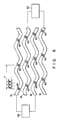
- a cell array pattern of dynamic memory cells shown in Figs. 1 and 2 is similar to that of the conventional dynamic memory cells explained with reference to Figs. 8 and 9 except that respective transistor contacts 63 of adjacent bit lines 61 are shifted by approximately 1/2 n (for example, 1/4) pitch in the bit line direction, and that the patterns of cell regions 11 have the same direction (that is, the patterns of cell regions 11 are of one kind).
- Fig. 1 shows part of the cell array pattern of folded bit line type as an example of a cell array pattern of dynamic memory cells with a one-transistor ⁇ one-capacitor structure in a dynamic memory. That is, in Fig. 1, 61 denotes bit lines arranged in parallel with one another, 62 denotes bit line sense amplifiers arranged at both ends of the bit lines 61. A sense amplifier 62 is successively connected to a complementary pair arrangement which includes adjacent bit lines 61 between which another bit line 61 is disposed. Each of the bit lines 61 has contacts 63, which are in contact with drain regions (or source regions) of cell transistors, at a regular interval of constant pitch P in its bit line direction. In this case, a distance between adjacent two contacts of the bit line is given as one pitch. The contacts 63 of the bit lines 61 are successively deviated from contacts 63 of an adjacent bit lines 61 by 1/4 pitch in the bit line direction.
- Fig. 2 shows part of the cell array pattern of Fig. 1 in detail.
- the bit lines 61 and word lines 72 are arranged in directions to intersect with each other, and each cell region 11 for two cell transistors is provided so as to traverse one desired bit line 61 and adjacent two word lines 72, respectively.
- the respective patterns of the cell regions 11 have the same direction, and one kind of the cell region patterns are repeatedly arranged as a whole.
- each of the bit lines 61 is in contact with a common region of two cell transistors every desired pitch in its longitudinal direction at portions intersecting with cell regions 11.
- the two cell transistors are provided so as to include two capacitors, thereby providing two dynamic memory cells with one-transistor ⁇ one-capacitor structure per one cell region.
- the transistor contacts 63 of one of the bit lines 61 are successively deviated by approximately 1/4 pitch in the bit line direction from the corresponding transistor contacts 63 of another bit lines 61 which are adjacent to the above bit line 61.
- a capacitor storage electrode 73 is provided every each memory cell and is in contact with a corresponding cell transistor.
- 74 denotes contacts between the source regions 43 or 44 of the cell transistors and the capacitor storage electrodes 73.
- Fig. 3 shows a pattern of the source regions 43 and 44, channel regions 12 and drain region 45 of the cell transistor pair in the cell region 11 shown in Fig. 2.
- Fig. 4 shows the cross section of the memory cell region of Fig. 2.
- 41 denotes a semiconductor substrate
- 42 denotes a field insulating film for cell isolation selectively formed in the substrate
- 43 and 44 denote the source regions of first and second cell transistors which are formed of diffused regions of a conductivity type opposite to that of the substrate
- 45 denotes the common drain region of the first and second cell transistors which is formed of a diffused region of a conductivity type opposite to that of the substrate
- 46 and 47 denote the gate electrodes of the first and second cell transistors which are disposed on a thin gate insulating film 48 provided on the substrate 41 and which are part of the word lines 72, respectively.
- 49 denotes a first interlevel insulator
- 61 denotes the bit lines
- 63 denotes the transistor contact which is in contact with the drain region 45 through a contact hole, respectively.
- 72 denotes the word lines and 50 denotes a second interlevel insulator.
- the first and second cell transistors include a charge storage capacitor, respectively. That is, capacitor storage electrodes denoted by 73 are partly disposed on the second interlevel insulator 50 so as to be located above part of the upper portion of the bit lines 61, and are in contact with the source regions 43 and 44 of the cell transistors through contact holes, respectively.
- a capacitor plate electrode 52 is provided so that the capacitor storage electrode 73 are faced through a thin capacitor insulating film 51, thereby providing a stacked capacitor.
- the cell regions 11 are provided by one kind of repeated patterns having the same directions.
- the integration density of the cell regions 11 is determined by the minimum distance dl between the adjacent patterns in the word line direction or by the minimum distance d2 between the adjacent patterns in the bit line direction, and since a distance between adjacent patterns, which are deviated from each other by approximately 1/4 pitch in the bit line direction, is reduced to of the order of the minimum distance d1 or d2, the density of the cell regions 11 can be increased, thereby further increasing the integration density thereof.
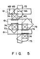
- the word line width Wa near the contact 74 may be made narrower than the word line width WA of the other portion thereof as shown in Fig. 5.
- the bit line width Wb near each contact 74 may be made narrower than the bit line width WB of the other portion thereof.
- part of the capacitor storage electrode 73 is provided above part of the bit line 61, but it may be located below part of the bit line 61.
- Figs. 6 and 7 show a cell array pattern of folded bit line type dynamic memory cells in which contacts of the adjacent bit lines are deviated from one another by 1/8 pitch, and the same parts or components as those of Fig. 2 are denoted by the same reference numerals.
- a sense amplifier 62 is successivelysively connected to both ends of bit lines which provide a complementary pair arrangement which includes adjacent bit lines 61 between which another bit line 61 is disposed.
- Each of the bit lines 61 has contacts 63, which are in contact with drain regions (or source regions) of cell transistors, at a regular interval of constant pitch P in its bit line direction.
- the contacts 63 of the bit lines 61 are successivelysively deviated from contacts 63 of adjacent bit lines 61 by 1/8 pitch in the bit line direction.
- Fig. 7 shows part of the cell array pattern of Fig. 6 in detail.
- the word lines 72 are insulatively disposed above the cell regions 11 formed in the semiconductor substrate, and the bit lines 61 are insulatively formed over the word lines.
- the cell regions 11 are formed of one kind of repeated patterns having the same direction.
- Each of the bit lines 61 are electrically connected to common regions of transistor pairs in cell regions 11 via the contacts 63, respectively.
- the contacts 63 of adjacent bit lines 61 are deviated by 1/8 pitch in the bit line direction from one another.
- An insulating film (not shown) is formed to cover the bit lines, and the capacitor storage electrodes 73 are provided on the insulating film.
- the storage electrodes 73 are connected to the source regions of corresponding cell transistors via the contacts 74.
- capacitor plate electrodes 52 are disposed to face the storage electrodes 73 via an insulating film.
- the basic structure is the same as that of the first embodiment except that the contacts 63 of the adjacent bit lines 61 are deviated from one another by 1/8 pitch in the bit line direction, and the pattern density of the cell regions can be further increased.
- this invention is not limited to the dynamic memory devices having the folded bit line type cell array pattern as described in the above embodiments, but can be applicable to dynamic memory devices using open bit line type cell array patterns.
Applications Claiming Priority (2)
| Application Number | Priority Date | Filing Date | Title |
|---|---|---|---|
| JP12991689 | 1989-05-23 | ||
| JP129916/89 | 1989-05-23 |
Publications (2)
| Publication Number | Publication Date |
|---|---|
| EP0399531A1 true EP0399531A1 (de) | 1990-11-28 |
| EP0399531B1 EP0399531B1 (de) | 1997-12-29 |
Family
ID=15021570
Family Applications (1)
| Application Number | Title | Priority Date | Filing Date |
|---|---|---|---|
| EP90109899A Expired - Lifetime EP0399531B1 (de) | 1989-05-23 | 1990-05-23 | Halbleiterspeicherbauteil |
Country Status (4)
| Country | Link |
|---|---|
| EP (1) | EP0399531B1 (de) |
| JP (1) | JPH07120714B2 (de) |
| KR (1) | KR930002289B1 (de) |
| DE (1) | DE69031847T2 (de) |
Cited By (10)
| Publication number | Priority date | Publication date | Assignee | Title |
|---|---|---|---|---|
| EP0428247A2 (de) * | 1989-08-19 | 1991-05-22 | Fujitsu Limited | Halbleiterspeicherbauteil mit verbessertem "Layout" der Kontakte |
| EP0449422A2 (de) * | 1990-02-26 | 1991-10-02 | Nec Corporation | Halbleiterspeicheranordnung |
| EP0464686A1 (de) * | 1990-07-06 | 1992-01-08 | Nec Corporation | Dynamische Halbleiterspeicherzelle |
| EP0464251A1 (de) * | 1990-07-06 | 1992-01-08 | Fujitsu Limited | Dynamischer Speicher mit wahlfreiem Zugriff mit verbessertem Layout und Methode zur Anordnung des Speicherzellenmusters |
| DE4139719C1 (de) * | 1991-12-02 | 1993-04-08 | Siemens Ag, 8000 Muenchen, De | |
| DE4335997A1 (de) * | 1992-10-21 | 1994-04-28 | Mitsubishi Electric Corp | Halbleiterspeichervorrichtung |
| EP0949681A1 (de) * | 1998-04-09 | 1999-10-13 | Nec Corporation | Halbleiterspeicheranordnung |
| EP0780901A3 (de) * | 1995-12-21 | 1999-11-10 | Texas Instruments Incorporated | Layout von DRAM-Speicherzellenanordnung |
| EP0967652A1 (de) * | 1998-06-26 | 1999-12-29 | Texas Instruments Incorporated | Layout von DRAM-Speicherzellenanordnung |
| CN110349960A (zh) * | 2019-07-08 | 2019-10-18 | 上海华虹宏力半导体制造有限公司 | 嵌入式闪存的版图结构、嵌入式闪存及其形成方法 |
Families Citing this family (7)
| Publication number | Priority date | Publication date | Assignee | Title |
|---|---|---|---|---|
| JP2515037B2 (ja) * | 1990-05-14 | 1996-07-10 | シャープ株式会社 | 半導体メモリ |
| JP2787852B2 (ja) * | 1991-04-15 | 1998-08-20 | 日本電気株式会社 | 半導体メモリ装置 |
| JP3666893B2 (ja) * | 1993-11-19 | 2005-06-29 | 株式会社日立製作所 | 半導体メモリ装置 |
| TW318281B (de) * | 1994-08-30 | 1997-10-21 | Mitsubishi Electric Corp | |
| JP2930110B2 (ja) * | 1996-11-14 | 1999-08-03 | 日本電気株式会社 | 半導体記憶装置およびその製造方法 |
| JP3292235B2 (ja) * | 1997-12-03 | 2002-06-17 | 日本電気株式会社 | 半導体装置 |
| DE19924567C2 (de) * | 1999-05-28 | 2003-04-30 | Infineon Technologies Ag | Integrierter Speicher mit 2-Transistor/2-Kondensator-Speicherzellen |
Citations (2)
| Publication number | Priority date | Publication date | Assignee | Title |
|---|---|---|---|---|
| EP0055572A2 (de) * | 1980-12-26 | 1982-07-07 | Fujitsu Limited | Halbleiterspeicheranordnung |
| US4700328A (en) * | 1985-07-11 | 1987-10-13 | Intel Corporation | High speed and high efficiency layout for dram circuits |
-
1990
- 1990-05-23 KR KR1019900007434A patent/KR930002289B1/ko not_active IP Right Cessation
- 1990-05-23 DE DE69031847T patent/DE69031847T2/de not_active Expired - Fee Related
- 1990-05-23 EP EP90109899A patent/EP0399531B1/de not_active Expired - Lifetime
- 1990-05-23 JP JP2131429A patent/JPH07120714B2/ja not_active Expired - Lifetime
Patent Citations (2)
| Publication number | Priority date | Publication date | Assignee | Title |
|---|---|---|---|---|
| EP0055572A2 (de) * | 1980-12-26 | 1982-07-07 | Fujitsu Limited | Halbleiterspeicheranordnung |
| US4700328A (en) * | 1985-07-11 | 1987-10-13 | Intel Corporation | High speed and high efficiency layout for dram circuits |
Non-Patent Citations (3)
| Title |
|---|
| IEDM 88 Technical Digest 1989, New York, U.S. pages 596 - 599; S. Kimura et al.: "A New Stacked Capacitor DRAM Cell" * |
| PATENT ABSTRACTS OF JAPAN vol. 13, no. 301 (E-785)(3649) 11 June 1989,& JP-A-01 080 068 (HITACHI LTD) 24 March 1989, * |
| PATENT ABSTRACTS OF JAPAN, vol. 13, no. 106 (E-726)[3454], 14th March 1989; & JP-A-63 278 363 (HITACHI) 16-11-1988 * |
Cited By (23)
| Publication number | Priority date | Publication date | Assignee | Title |
|---|---|---|---|---|
| EP0756327A1 (de) * | 1989-08-19 | 1997-01-29 | Fujitsu Limited | Halbleiter-Speicherbauteil mit Bitleitungskontaktfläche und Speicherelektrodenkontaktfläche |
| EP0428247A3 (en) * | 1989-08-19 | 1991-12-04 | Fujitsu Limited | Semiconductor memory device with improved contact layout |
| EP0428247A2 (de) * | 1989-08-19 | 1991-05-22 | Fujitsu Limited | Halbleiterspeicherbauteil mit verbessertem "Layout" der Kontakte |
| US6026010A (en) * | 1989-08-19 | 2000-02-15 | Fujitsu Limited | Semiconductor memory device with bit line contact areas and storage capacitor contact areas |
| US5812444A (en) * | 1989-08-19 | 1998-09-22 | Fujitsu Limited | Semiconductor memory device with bit line contact areas and storage capacitor contact areas |
| EP0449422A2 (de) * | 1990-02-26 | 1991-10-02 | Nec Corporation | Halbleiterspeicheranordnung |
| EP0449422B1 (de) * | 1990-02-26 | 1997-06-18 | Nec Corporation | Halbleiterspeicheranordnung |
| EP0464686A1 (de) * | 1990-07-06 | 1992-01-08 | Nec Corporation | Dynamische Halbleiterspeicherzelle |
| EP0464251A1 (de) * | 1990-07-06 | 1992-01-08 | Fujitsu Limited | Dynamischer Speicher mit wahlfreiem Zugriff mit verbessertem Layout und Methode zur Anordnung des Speicherzellenmusters |
| US5305252A (en) * | 1990-07-06 | 1994-04-19 | Nec Corporation | Semiconductor memory device having memory cell matrix obliquely arranged with respect to bit lines |
| EP0684649A2 (de) * | 1990-07-06 | 1995-11-29 | Fujitsu Limited | Dynamischer Speicher mit wahlfreiem Zugriff |
| EP0684649A3 (de) * | 1990-07-06 | 1996-05-08 | Fujitsu Ltd | Dynamischer Speicher mit wahlfreiem Zugriff. |
| DE4139719C1 (de) * | 1991-12-02 | 1993-04-08 | Siemens Ag, 8000 Muenchen, De | |
| US5315542A (en) * | 1991-12-02 | 1994-05-24 | Siemens Aktiengesellschaft | Bit line arrangement for integrated circuits |
| EP0545256A1 (de) * | 1991-12-02 | 1993-06-09 | Siemens Aktiengesellschaft | Bitleitungsanordnung für integrierte Schaltungen |
| KR100279485B1 (ko) * | 1991-12-02 | 2001-03-02 | 칼 하인쯔 호르닝어 | 집적 회로의 비트 라인 장치 |
| DE4335997A1 (de) * | 1992-10-21 | 1994-04-28 | Mitsubishi Electric Corp | Halbleiterspeichervorrichtung |
| EP0780901A3 (de) * | 1995-12-21 | 1999-11-10 | Texas Instruments Incorporated | Layout von DRAM-Speicherzellenanordnung |
| EP0949681A1 (de) * | 1998-04-09 | 1999-10-13 | Nec Corporation | Halbleiterspeicheranordnung |
| US6185120B1 (en) | 1998-04-09 | 2001-02-06 | Nec Corporation | Semiconductor memory device |
| EP0967652A1 (de) * | 1998-06-26 | 1999-12-29 | Texas Instruments Incorporated | Layout von DRAM-Speicherzellenanordnung |
| US6166941A (en) * | 1998-06-26 | 2000-12-26 | Texas Instruments Incorporated | Relaxed layout for storage nodes for dynamic random access memories |
| CN110349960A (zh) * | 2019-07-08 | 2019-10-18 | 上海华虹宏力半导体制造有限公司 | 嵌入式闪存的版图结构、嵌入式闪存及其形成方法 |
Also Published As
| Publication number | Publication date |
|---|---|
| DE69031847D1 (de) | 1998-02-05 |
| EP0399531B1 (de) | 1997-12-29 |
| JPH07120714B2 (ja) | 1995-12-20 |
| KR930002289B1 (ko) | 1993-03-29 |
| JPH0372675A (ja) | 1991-03-27 |
| DE69031847T2 (de) | 1998-05-14 |
| KR900019238A (ko) | 1990-12-24 |
Similar Documents
| Publication | Publication Date | Title |
|---|---|---|
| EP0399531A1 (de) | Halbleiterspeicherbauteil | |
| US5691551A (en) | Semiconductor memory device | |
| US5504028A (en) | Method of forming a dynamic random memory device | |
| US5194752A (en) | Semiconductor memory device | |
| US5747844A (en) | Dynamic semiconductor memory device with higher density bit line/word line layout | |
| US4012757A (en) | Contactless random-access memory cell and cell pair | |
| EP0169332B1 (de) | Hochverdichtete Speicher mit Einzelelementspeicherzellen | |
| US4860070A (en) | Semiconductor memory device comprising trench memory cells | |
| JP2508288B2 (ja) | 半導体記憶装置 | |
| US6784502B2 (en) | Method of forming contacts, methods of contacting lines, methods of operating integrated circuitry, and integrated circuits | |
| US4959698A (en) | Memory cell of a semiconductor memory device | |
| KR940010833B1 (ko) | 다이나믹형 반도체메모리 | |
| US5016071A (en) | Dynamic memory device | |
| KR850005172A (ko) | 직렬접속한 misfet와 캐파시터를 가진 반도체 집적회로 장치 | |
| US5506428A (en) | Gate array LSI | |
| US6282116B1 (en) | Dynamic random access memory | |
| EP0234741B1 (de) | Halbleiterspeichervorrichtung | |
| KR100291009B1 (ko) | 반도체메모리장치용주변회로 | |
| US6388283B1 (en) | Semiconductor memory with a strip-shaped cell plate | |
| JPS62150879A (ja) | 半導体記憶装置 | |
| US4173819A (en) | Method of manufacturing a dynamic random access memory using MOS FETS | |
| EP0817269A3 (de) | Wortleitungsanordnung für Halbleiter-Speicherbauteil | |
| EP0780901A2 (de) | Layout von DRAM-Speicherzellenanordnung | |
| US5748549A (en) | Semiconductor memory device | |
| GB2312094A (en) | Stacked capacitor type DRAM |
Legal Events
| Date | Code | Title | Description |
|---|---|---|---|
| PUAI | Public reference made under article 153(3) epc to a published international application that has entered the european phase |
Free format text: ORIGINAL CODE: 0009012 |
|
| 17P | Request for examination filed |
Effective date: 19900523 |
|
| AK | Designated contracting states |
Kind code of ref document: A1 Designated state(s): DE FR GB |
|
| 17Q | First examination report despatched |
Effective date: 19931105 |
|
| GRAG | Despatch of communication of intention to grant |
Free format text: ORIGINAL CODE: EPIDOS AGRA |
|
| GRAG | Despatch of communication of intention to grant |
Free format text: ORIGINAL CODE: EPIDOS AGRA |
|
| GRAH | Despatch of communication of intention to grant a patent |
Free format text: ORIGINAL CODE: EPIDOS IGRA |
|
| GRAH | Despatch of communication of intention to grant a patent |
Free format text: ORIGINAL CODE: EPIDOS IGRA |
|
| GRAA | (expected) grant |
Free format text: ORIGINAL CODE: 0009210 |
|
| AK | Designated contracting states |
Kind code of ref document: B1 Designated state(s): DE FR GB |
|
| REF | Corresponds to: |
Ref document number: 69031847 Country of ref document: DE Date of ref document: 19980205 |
|
| ET | Fr: translation filed | ||
| REG | Reference to a national code |
Ref country code: GB Ref legal event code: 746 Effective date: 19981012 |
|
| PLBE | No opposition filed within time limit |
Free format text: ORIGINAL CODE: 0009261 |
|
| STAA | Information on the status of an ep patent application or granted ep patent |
Free format text: STATUS: NO OPPOSITION FILED WITHIN TIME LIMIT |
|
| 26N | No opposition filed | ||
| REG | Reference to a national code |
Ref country code: FR Ref legal event code: D6 |
|
| REG | Reference to a national code |
Ref country code: GB Ref legal event code: IF02 |
|
| PGFP | Annual fee paid to national office [announced via postgrant information from national office to epo] |
Ref country code: FR Payment date: 20020508 Year of fee payment: 13 |
|
| PGFP | Annual fee paid to national office [announced via postgrant information from national office to epo] |
Ref country code: GB Payment date: 20020522 Year of fee payment: 13 |
|
| PG25 | Lapsed in a contracting state [announced via postgrant information from national office to epo] |
Ref country code: GB Free format text: LAPSE BECAUSE OF NON-PAYMENT OF DUE FEES Effective date: 20030523 |
|
| GBPC | Gb: european patent ceased through non-payment of renewal fee |
Effective date: 20030523 |
|
| PG25 | Lapsed in a contracting state [announced via postgrant information from national office to epo] |
Ref country code: FR Free format text: LAPSE BECAUSE OF NON-PAYMENT OF DUE FEES Effective date: 20040130 |
|
| REG | Reference to a national code |
Ref country code: FR Ref legal event code: ST |
|
| PGFP | Annual fee paid to national office [announced via postgrant information from national office to epo] |
Ref country code: DE Payment date: 20070517 Year of fee payment: 18 |
|
| PG25 | Lapsed in a contracting state [announced via postgrant information from national office to epo] |
Ref country code: DE Free format text: LAPSE BECAUSE OF NON-PAYMENT OF DUE FEES Effective date: 20081202 |