EP0398366A2 - Halbleiterbehandlungsvorrichtung und Verfahren - Google Patents
Halbleiterbehandlungsvorrichtung und Verfahren Download PDFInfo
- Publication number
- EP0398366A2 EP0398366A2 EP90109478A EP90109478A EP0398366A2 EP 0398366 A2 EP0398366 A2 EP 0398366A2 EP 90109478 A EP90109478 A EP 90109478A EP 90109478 A EP90109478 A EP 90109478A EP 0398366 A2 EP0398366 A2 EP 0398366A2
- Authority
- EP
- European Patent Office
- Prior art keywords
- susceptor
- chamber
- substrate
- loading
- reaction chamber
- Prior art date
- Legal status (The legal status is an assumption and is not a legal conclusion. Google has not performed a legal analysis and makes no representation as to the accuracy of the status listed.)
- Granted
Links
Images
Classifications
-
- C—CHEMISTRY; METALLURGY
- C23—COATING METALLIC MATERIAL; COATING MATERIAL WITH METALLIC MATERIAL; CHEMICAL SURFACE TREATMENT; DIFFUSION TREATMENT OF METALLIC MATERIAL; COATING BY VACUUM EVAPORATION, BY SPUTTERING, BY ION IMPLANTATION OR BY CHEMICAL VAPOUR DEPOSITION, IN GENERAL; INHIBITING CORROSION OF METALLIC MATERIAL OR INCRUSTATION IN GENERAL
- C23C—COATING METALLIC MATERIAL; COATING MATERIAL WITH METALLIC MATERIAL; SURFACE TREATMENT OF METALLIC MATERIAL BY DIFFUSION INTO THE SURFACE, BY CHEMICAL CONVERSION OR SUBSTITUTION; COATING BY VACUUM EVAPORATION, BY SPUTTERING, BY ION IMPLANTATION OR BY CHEMICAL VAPOUR DEPOSITION, IN GENERAL
- C23C16/00—Chemical coating by decomposition of gaseous compounds, without leaving reaction products of surface material in the coating, i.e. chemical vapour deposition [CVD] processes
- C23C16/44—Chemical coating by decomposition of gaseous compounds, without leaving reaction products of surface material in the coating, i.e. chemical vapour deposition [CVD] processes characterised by the method of coating
- C23C16/54—Apparatus specially adapted for continuous coating
-
- C—CHEMISTRY; METALLURGY
- C23—COATING METALLIC MATERIAL; COATING MATERIAL WITH METALLIC MATERIAL; CHEMICAL SURFACE TREATMENT; DIFFUSION TREATMENT OF METALLIC MATERIAL; COATING BY VACUUM EVAPORATION, BY SPUTTERING, BY ION IMPLANTATION OR BY CHEMICAL VAPOUR DEPOSITION, IN GENERAL; INHIBITING CORROSION OF METALLIC MATERIAL OR INCRUSTATION IN GENERAL
- C23C—COATING METALLIC MATERIAL; COATING MATERIAL WITH METALLIC MATERIAL; SURFACE TREATMENT OF METALLIC MATERIAL BY DIFFUSION INTO THE SURFACE, BY CHEMICAL CONVERSION OR SUBSTITUTION; COATING BY VACUUM EVAPORATION, BY SPUTTERING, BY ION IMPLANTATION OR BY CHEMICAL VAPOUR DEPOSITION, IN GENERAL
- C23C16/00—Chemical coating by decomposition of gaseous compounds, without leaving reaction products of surface material in the coating, i.e. chemical vapour deposition [CVD] processes
- C23C16/44—Chemical coating by decomposition of gaseous compounds, without leaving reaction products of surface material in the coating, i.e. chemical vapour deposition [CVD] processes characterised by the method of coating
- C23C16/4401—Means for minimising impurities, e.g. dust, moisture or residual gas, in the reaction chamber
-
- H—ELECTRICITY
- H10—SEMICONDUCTOR DEVICES; ELECTRIC SOLID-STATE DEVICES NOT OTHERWISE PROVIDED FOR
- H10P—GENERIC PROCESSES OR APPARATUS FOR THE MANUFACTURE OR TREATMENT OF DEVICES COVERED BY CLASS H10
- H10P72/00—Handling or holding of wafers, substrates or devices during manufacture or treatment thereof
- H10P72/70—Handling or holding of wafers, substrates or devices during manufacture or treatment thereof for supporting or gripping
- H10P72/76—Handling or holding of wafers, substrates or devices during manufacture or treatment thereof for supporting or gripping using mechanical means, e.g. clamps or pinches
- H10P72/7604—Handling or holding of wafers, substrates or devices during manufacture or treatment thereof for supporting or gripping using mechanical means, e.g. clamps or pinches the wafers being placed on a susceptor, stage or support
- H10P72/7618—Handling or holding of wafers, substrates or devices during manufacture or treatment thereof for supporting or gripping using mechanical means, e.g. clamps or pinches the wafers being placed on a susceptor, stage or support characterised by a movable susceptor, stage or support, others than those only rotating on their own vertical axis, e.g. susceptors on a rotating carrousel
-
- C—CHEMISTRY; METALLURGY
- C30—CRYSTAL GROWTH
- C30B—SINGLE-CRYSTAL GROWTH; UNIDIRECTIONAL SOLIDIFICATION OF EUTECTIC MATERIAL OR UNIDIRECTIONAL DEMIXING OF EUTECTOID MATERIAL; REFINING BY ZONE-MELTING OF MATERIAL; PRODUCTION OF A HOMOGENEOUS POLYCRYSTALLINE MATERIAL WITH DEFINED STRUCTURE; SINGLE CRYSTALS OR HOMOGENEOUS POLYCRYSTALLINE MATERIAL WITH DEFINED STRUCTURE; AFTER-TREATMENT OF SINGLE CRYSTALS OR A HOMOGENEOUS POLYCRYSTALLINE MATERIAL WITH DEFINED STRUCTURE; APPARATUS THEREFOR
- C30B25/00—Single-crystal growth by chemical reaction of reactive gases, e.g. chemical vapour-deposition growth
- C30B25/02—Epitaxial-layer growth
-
- C—CHEMISTRY; METALLURGY
- C30—CRYSTAL GROWTH
- C30B—SINGLE-CRYSTAL GROWTH; UNIDIRECTIONAL SOLIDIFICATION OF EUTECTIC MATERIAL OR UNIDIRECTIONAL DEMIXING OF EUTECTOID MATERIAL; REFINING BY ZONE-MELTING OF MATERIAL; PRODUCTION OF A HOMOGENEOUS POLYCRYSTALLINE MATERIAL WITH DEFINED STRUCTURE; SINGLE CRYSTALS OR HOMOGENEOUS POLYCRYSTALLINE MATERIAL WITH DEFINED STRUCTURE; AFTER-TREATMENT OF SINGLE CRYSTALS OR A HOMOGENEOUS POLYCRYSTALLINE MATERIAL WITH DEFINED STRUCTURE; APPARATUS THEREFOR
- C30B35/00—Apparatus not otherwise provided for, specially adapted for the growth, production or after-treatment of single crystals or of a homogeneous polycrystalline material with defined structure
- C30B35/005—Transport systems
-
- H—ELECTRICITY
- H10—SEMICONDUCTOR DEVICES; ELECTRIC SOLID-STATE DEVICES NOT OTHERWISE PROVIDED FOR
- H10P—GENERIC PROCESSES OR APPARATUS FOR THE MANUFACTURE OR TREATMENT OF DEVICES COVERED BY CLASS H10
- H10P72/00—Handling or holding of wafers, substrates or devices during manufacture or treatment thereof
- H10P72/70—Handling or holding of wafers, substrates or devices during manufacture or treatment thereof for supporting or gripping
- H10P72/76—Handling or holding of wafers, substrates or devices during manufacture or treatment thereof for supporting or gripping using mechanical means, e.g. clamps or pinches
- H10P72/7602—Handling or holding of wafers, substrates or devices during manufacture or treatment thereof for supporting or gripping using mechanical means, e.g. clamps or pinches the wafers being placed on a robot blade or gripped by a gripper for conveyance
-
- H—ELECTRICITY
- H10—SEMICONDUCTOR DEVICES; ELECTRIC SOLID-STATE DEVICES NOT OTHERWISE PROVIDED FOR
- H10P—GENERIC PROCESSES OR APPARATUS FOR THE MANUFACTURE OR TREATMENT OF DEVICES COVERED BY CLASS H10
- H10P72/00—Handling or holding of wafers, substrates or devices during manufacture or treatment thereof
- H10P72/70—Handling or holding of wafers, substrates or devices during manufacture or treatment thereof for supporting or gripping
- H10P72/76—Handling or holding of wafers, substrates or devices during manufacture or treatment thereof for supporting or gripping using mechanical means, e.g. clamps or pinches
- H10P72/7604—Handling or holding of wafers, substrates or devices during manufacture or treatment thereof for supporting or gripping using mechanical means, e.g. clamps or pinches the wafers being placed on a susceptor, stage or support
- H10P72/7621—Handling or holding of wafers, substrates or devices during manufacture or treatment thereof for supporting or gripping using mechanical means, e.g. clamps or pinches the wafers being placed on a susceptor, stage or support characterised by supporting two or more semiconductor substrates
Definitions
- the present invention relates generally to the field of silicon wafer fabrication equipment useful in the manufacture of semiconductor devices, more particularly to apparatus for depositing an epitaxial layer from a source gas by the chemical vapor deposition (CVD) method, and especially to improvements in such apparatus when used with robotic loading of wafers.
- CVD chemical vapor deposition
- Apparatus of the above type is used in the fabrication of semiconductor devices on 100 millimeter or larger wafers of silicon. Epitaxial layers are formed on the surfaces of the wafers by heating them to temperatures in the region of 1100 to 1200 degrees Celsius in a bell jar containing a gaseous atmosphere consisting of a hydrogen carrier gas mixed with one or more reactive gases such as a silicon source gas or a dopant source gas.
- a robotic loader In order to provide automatic processing of a large number of wafers, a robotic loader, together with the necessary control electronics, can be used to automatically load unprocessed wafers onto the susceptor which is used to support them. The susceptor is then loaded into the reaction chamber, processing is carried out, and the susceptor is removed from the reaction chamber, whereupon the robot removes the processed wafers from the susceptor and loads unprocessed wafers.
- the known prior art is exemplified by automated epitaxial reactor systems of the type represented by the Model 7010 system supplied by Applied Materials of Santa Clara, California. This system uses a robotic loader to load and unload substrates from the susceptor.
- This system permit supporting the susceptor quite rigidly from its base.
- a stream of filtered air sweeps over the susceptor surface to remove corrosive vapors such as chlorides which are byproducts of the CVD process.
- a method for handling and supporting semiconductor wafers comprising:
- the susceptor is supported from a single point near its upper end by a suspension mount which provides sufficient compliance to permit the susceptor to center itself below the mount through gravitational force alone.
- a suspension mount which provides sufficient compliance to permit the susceptor to center itself below the mount through gravitational force alone.
- the present invention provides an automated epitaxial reactor system having a greater capacity than the prior art systems.
- the present invention further provides such a system in which the efficiency of removal of harmful process byproducts is enhanced.
- the present invention also provides a system with a self-centering susceptor for supporting substrates.
- the present invention further provides a system with a means to support and fix the position of the susceptor during substrate loading operations.
- the present invention further provides a system with a means to catch a substrate which is accidentally dropped during the operations of loading or unloading substrates, and to thereby prevent damage to the system.
- the present invention further provides a system having a susceptor stabilization means in a form which can be extended toward the susceptor at the start of substrate loading and withdrawn at the end of substrate loading.
- the present invention also provides a system in which susceptor stabilization and removal of harmful process byproducts is accomplished by a single movable element.
- an automated epitaxial vapor deposition apparatus uses an elongated, multi-sided susceptor which is suspended by a centrally located gimballed mounting at its top end.
- the susceptor has sufficient axial length to accommodate two or more substrates on each of its sides.
- the susceptor is lowered into a bell jar for processing and raised from the bell jar for loading and unloading of semiconductor substrates. Consequently, the loading of substrates is carried out while the susceptor is suspended directly over the open mouth of the bell jar.
- the gimballed upper support of the susceptor has considerable compliance to permit the susceptor to self-center when it is in the bell jar, such that the susceptor can be rotated during processing without significant eccentricity.
- the same compliance comprises a drawback during the operation of loading and unloading substrates by means of a robotic loader.
- the filtered air stream which is used to aid in the removal of noxious vapors has the additional and unwanted effect of causing the susceptor to swing, making loading of the substrates difficult.
- a susceptor stabilization means in the form of a carriage which is movable toward and away from the susceptor carries on its upper surface a pair of compliant contactor pads for frictionally engaging the lower end of the susceptor.
- the same carriage also incorporates a vacuum duct extending from an opening located on the underside of the carriage, adjacent the mouth of the bell jar, to a remotely located source of low vacuum. Consequently, when the carriage is extended into position below the susceptor, the opening on its underside draws noxious and corrosive vapors and particulate matter from the open mouth of the bell jar.
- the carriage is withdrawn, permitting the loaded susceptor to be lowered into the bell jar.
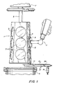
- a graphite susceptor 1 is shown as it would appear during the operation of loading and unloading semiconductor wafers 3.
- Susceptor 1 is, for example, an elongated, five-sided support structure having three wafers 3 retained in correspondingly-shaped recesses on each of its sides. As illustrated, susceptor 1 has a slight axial taper, such that it is larger at the bottom than at the top. Formed in this way, each of the sides of susceptor 1 slopes in a sense to provide a small radially inward gravitational force component on each of wafers 3 to prevent accidental dislodging of the wafers during processing.
- a support hanger 5 in the form of a short stub shaft, connects susceptor 1 to a rotatable support structure 7 which can be raised to the illustrated loading position and lowered to load susceptor 1 into a reaction chamber or bell jar 9 for processing.
- susceptor 1 and wafers 3 are subjected to temperatures in the region of 1100 to 1200 degrees Celsius in a reactive gaseous environment.
- susceptor 1 is rotated to agitate and stir the gaseous mixture.
- Such stirring action is effective at maintaining a uniform gaseous mixture only if susceptor 1 remains centered such that its axis coincides with the axis of rotation. Accordingly, support hanger is supported within support structure 7 in a manner which provides considerable compliance, such that susceptor 1 will self-center by gravitational force as will become clearer from the later discussion of Fig. 2.
- Loading of unprocessed substrates and unloading of processed ones is carried out by a robotic loader 11 which is illustrated somewhat schematically in Fig. 1.
- Loader 11 is equipped with four fingers 13, only two of which are shown in Fig. 1, for gripping each substrate by its edges.
- Loader 11 uses a system of infrared sensors (not shown) in order to accurately map the locations of each of the three substrates on each side of susceptor 1. As each of the five sides of susceptor 1 is completed, hanger 5 is rotated to access the next side, whereupon loader 11 begins the operation of loading by storing data which determines the exact location of each of the three substrates on the side.
- loader 11 can efficiently complete the loading of all three substrates without pausing to relocate the appropriate recesses.
- susceptor 1 must remain stationary throughout the loading of each side in order that the location data stored prior to loading remain valid throughout the loading operation.
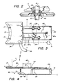
- susceptor 1 can be maintained in a fixed position throughout the operation of loading each of its sides by the use of a susceptor stabilizer 15 which can be selectively engaged at the start of the loading operation on each side and disengaged when necessary to rotate susceptor 1.
- Stabilizer 15 can be simply and effectively realized in a form which engages susceptor 1 at its lower edge, as illustrated in Fig. 1. When thus engaged, susceptor 1 is supported at widely separated points located at its top and bottom, and is firmly fixed during the loading operation.
- stabilizer 15 Although the structure of stabilizer 15 will be fully discussed with respect to Figs. 3 and 4, it may be noted here that engagement of stabilizer 15 with susceptor 1 is accomplished simply by pressing a pair of frictional contactors 17 (only one of which is visible in Fig. 1) firmly against the lower edge of susceptor 1. For this purpose a lift arm 19, raised and lowered by a pneumatic lift cylinder which will be described later with respect to Fig. 4, is used to raise and lower stabilizer 15 during the loading of susceptor 1.
- Support hanger 5 is suspended from a driving shaft 21 by a mounting ring 23 and a pair of trunnion pins 25 and 27.
- Mounting ring 23 and trunnion pins 25 and 27 together form a gimballed joint which provides sufficient compliance to accommodate a slight misalignment between shafts 5 and 21, and to thus permit susceptor 1 to self-center through the action of gravity.
- Rotation of susceptor 1 both during processing and during the substrate loading operation is accomplished by rotating shaft 21 such that the rotary motion is transmitted through the gimballed joint.
- ensuring that each of the sides of susceptor 1 is correctly oriented facing the robotic loader 11 of Fig. 1 requires that the location of these sides be known in relation to the rotational position of shaft 21.
- a second pin azimuthally displaced from pin 25 by an angle which is not 90 degrees, extends through ring 23 and shaft 21 for the purpose of ensuring that susceptor 1 can only be mounted with its sides in a preordained orientation.
- Fig. 3 illustrates the structure of stabilizer 15 in top view
- Fig. 4 shows the same structure from the side.
- a platform 29 is pivotally supported on a pair of upright posts 31 which are joined to a base 33.
- a stop 35 is also joined to base 33, and serves to limit the downward pivotal motion of platform 29 to the position illustrated, with platform 29 parallel to base 33.
- a movable shuttle or carriage 36 is supported upon a pair of traveling rods 37 which are in turn supported within four ball slides 39 mounted on platform 29.
- Carriage 36 is shown extended to the left in Figs. 1, 3, and 4 as it would be when in use to stabilize susceptor 1. However, carriage 36 is movable to the right as indicated by the phantom outline 41 in Fig. 4, such that its full range of motion is as indicated by arrow 43.
- a pneumatic cylinder 45 is used to drive carriage 36 either to the left or right in the drawing by applying air pressure to either of a pair of air pressure lines 47a or 47b.
- the entire stabilizer assembly consisting of platform 29, carriage 36, rods 37, slides 39 and cylinder 45 can be raised and lowered by a pneumatic lift cylinder 49 to cause contactor pads 17 to press against the lower edge of susceptor 1.
- switches 51 and 53 are shown coupled to carriage 36 by a dotted line. Whenever carriage 36 is lowered away from susceptor 1, the contacts of switch 53 are closed. Similarly, whenever carriage 36 is withdrawn from the region of susceptor 1 (i.e., moved all the way to the right in the figures), the contacts of switch 51 are closed. Accordingly, by sensing the states of switches 51 and 53, the computer can determine when susceptor 1 can safely be rotated to permit accessing a different side thereof.
- Carriage 36 is formed as a hollow member, having a lower wall identical to the upper wall illustrated in Fig. 3 with the exception that the leftmost edge of the lower wall, as indicated by dotted line 57, is undercut to form a downwardly oriented vacuum opening.
- carriage 36 serves as a portion of the vacuum duct.
- corrosive vapors and particulate matter within bell jar 9 are drawn into carriage 36, through duct 55, and are collected by the remote vacuum system.
Landscapes
- Chemical & Material Sciences (AREA)
- Engineering & Computer Science (AREA)
- Materials Engineering (AREA)
- Metallurgy (AREA)
- Organic Chemistry (AREA)
- General Chemical & Material Sciences (AREA)
- Chemical Kinetics & Catalysis (AREA)
- Mechanical Engineering (AREA)
- Crystallography & Structural Chemistry (AREA)
- Container, Conveyance, Adherence, Positioning, Of Wafer (AREA)
- Chemical Vapour Deposition (AREA)
Applications Claiming Priority (2)
| Application Number | Priority Date | Filing Date | Title |
|---|---|---|---|
| US354161 | 1989-05-19 | ||
| US07/354,161 US5116181A (en) | 1989-05-19 | 1989-05-19 | Robotically loaded epitaxial deposition apparatus |
Publications (3)
| Publication Number | Publication Date |
|---|---|
| EP0398366A2 true EP0398366A2 (de) | 1990-11-22 |
| EP0398366A3 EP0398366A3 (de) | 1991-06-12 |
| EP0398366B1 EP0398366B1 (de) | 1994-09-21 |
Family
ID=23392113
Family Applications (1)
| Application Number | Title | Priority Date | Filing Date |
|---|---|---|---|
| EP90109478A Expired - Lifetime EP0398366B1 (de) | 1989-05-19 | 1990-05-18 | Halbleiterbehandlungsvorrichtung und Verfahren |
Country Status (5)
| Country | Link |
|---|---|
| US (3) | US5116181A (de) |
| EP (1) | EP0398366B1 (de) |
| JP (1) | JP2693623B2 (de) |
| KR (1) | KR100189645B1 (de) |
| DE (1) | DE69012647T2 (de) |
Cited By (1)
| Publication number | Priority date | Publication date | Assignee | Title |
|---|---|---|---|---|
| WO2019096515A1 (en) * | 2017-11-15 | 2019-05-23 | Evatec Ag | Vacuum treatment apparatus and method of vacuum treating substrates |
Families Citing this family (18)
| Publication number | Priority date | Publication date | Assignee | Title |
|---|---|---|---|---|
| JPH081922B2 (ja) * | 1991-01-25 | 1996-01-10 | 株式会社東芝 | ウェハ−保持装置 |
| US5490881A (en) * | 1992-11-02 | 1996-02-13 | Gen Electric | Maintaining uniformity of deposited film thickness in plasma-enhanced chemical vapor deposition |
| US5458322A (en) * | 1994-03-25 | 1995-10-17 | Kulkaski; Richard | Debris trapping/anti clip for retaining a semiconductor wafer on a pedestal |
| US5657975A (en) * | 1995-03-25 | 1997-08-19 | Szapucki; Matthew Peter | Clip head apparatus for retaining a semiconductor wafer on a pedestal |
| US6129048A (en) * | 1998-06-30 | 2000-10-10 | Memc Electronic Materials, Inc. | Susceptor for barrel reactor |
| DE102006006231A1 (de) * | 2006-02-09 | 2007-08-23 | Kba-Metronic Ag | Transportträger zum Transport von Objekten entlang eines Behandlungsweges und Verfahren zur Zentrierung von Objekten in Transportträgern |
| US8430965B2 (en) * | 2007-02-16 | 2013-04-30 | Pronomic Industry Ab | Epitaxial growth system for fast heating and cooling |
| US20080314319A1 (en) * | 2007-06-19 | 2008-12-25 | Memc Electronic Materials, Inc. | Susceptor for improving throughput and reducing wafer damage |
| US8404049B2 (en) * | 2007-12-27 | 2013-03-26 | Memc Electronic Materials, Inc. | Epitaxial barrel susceptor having improved thickness uniformity |
| US20100098519A1 (en) * | 2008-10-17 | 2010-04-22 | Memc Electronic Materials, Inc. | Support for a semiconductor wafer in a high temperature environment |
| TW201122148A (en) * | 2009-12-24 | 2011-07-01 | Hon Hai Prec Ind Co Ltd | Chemical vapor deposition device |
| US9441295B2 (en) * | 2010-05-14 | 2016-09-13 | Solarcity Corporation | Multi-channel gas-delivery system |
| US9162245B1 (en) * | 2012-03-29 | 2015-10-20 | BTD Wood Powder Coating, Inc. | Powder coating conveyor support |
| US9972740B2 (en) | 2015-06-07 | 2018-05-15 | Tesla, Inc. | Chemical vapor deposition tool and process for fabrication of photovoltaic structures |
| US20170182636A1 (en) * | 2015-12-29 | 2017-06-29 | Vision Wide Tech Co., Ltd. | Precision protection jig with fat u-shaped base |
| US9748434B1 (en) | 2016-05-24 | 2017-08-29 | Tesla, Inc. | Systems, method and apparatus for curing conductive paste |
| US9954136B2 (en) | 2016-08-03 | 2018-04-24 | Tesla, Inc. | Cassette optimized for an inline annealing system |
| US10115856B2 (en) | 2016-10-31 | 2018-10-30 | Tesla, Inc. | System and method for curing conductive paste using induction heating |
Family Cites Families (14)
| Publication number | Priority date | Publication date | Assignee | Title |
|---|---|---|---|---|
| US3850138A (en) * | 1972-06-22 | 1974-11-26 | Varian Spa Leini | Substrate carrying apparatus for use in coating equipment |
| US3933572A (en) * | 1973-12-11 | 1976-01-20 | The United States Of America As Represented By The Secretary Of The Air Force | Method for growing crystals |
| US4329938A (en) * | 1980-10-03 | 1982-05-18 | The United States Of America As Represented By The Secretary Of The Navy | Evaporator tool with remote substrate reorientation mechanism |
| US4496828A (en) * | 1983-07-08 | 1985-01-29 | Ultra Carbon Corporation | Susceptor assembly |
| EP0189279B1 (de) * | 1985-01-22 | 1991-10-09 | Applied Materials, Inc. | Halbleiter-Bearbeitungseinrichtung |
| US4757890A (en) * | 1985-04-19 | 1988-07-19 | Motoda Denshi Kogyo Kabushiki Kaisha | Tray positioning arrangement for delivery system |
| US4823736A (en) * | 1985-07-22 | 1989-04-25 | Air Products And Chemicals, Inc. | Barrel structure for semiconductor epitaxial reactor |
| FR2590879A1 (fr) * | 1985-11-27 | 1987-06-05 | American Telephone & Telegraph | Procede et appareil pour le chargement et le dechargement automatiques de tranches de semi-conducteur |
| JPH0815540B2 (ja) * | 1985-12-27 | 1996-02-21 | 株式会社日立製作所 | 処理装置 |
| JPS62230973A (ja) * | 1986-03-31 | 1987-10-09 | Hitachi Metals Ltd | スパツタリング装置のデイスク移載方法 |
| US4904153A (en) * | 1986-11-20 | 1990-02-27 | Shimizu Construction Co., Ltd. | Transporting robot for semiconductor wafers |
| DE3707672A1 (de) * | 1987-03-10 | 1988-09-22 | Sitesa Sa | Epitaxieanlage |
| US5078091A (en) * | 1988-06-23 | 1992-01-07 | Jeffrey Stewart | Parylene deposition chamber and method of use |
| US4928626A (en) * | 1989-05-19 | 1990-05-29 | Applied Materials, Inc. | Reactant gas injection for IC processing |
-
1989
- 1989-05-19 US US07/354,161 patent/US5116181A/en not_active Expired - Fee Related
-
1990
- 1990-05-02 JP JP2116699A patent/JP2693623B2/ja not_active Expired - Fee Related
- 1990-05-18 DE DE69012647T patent/DE69012647T2/de not_active Expired - Fee Related
- 1990-05-18 EP EP90109478A patent/EP0398366B1/de not_active Expired - Lifetime
- 1990-05-19 KR KR1019900007200A patent/KR100189645B1/ko not_active Expired - Fee Related
-
1992
- 1992-10-29 US US07/968,223 patent/US5476359A/en not_active Expired - Fee Related
-
1993
- 1993-04-08 US US08/044,919 patent/US5374159A/en not_active Expired - Lifetime
Cited By (1)
| Publication number | Priority date | Publication date | Assignee | Title |
|---|---|---|---|---|
| WO2019096515A1 (en) * | 2017-11-15 | 2019-05-23 | Evatec Ag | Vacuum treatment apparatus and method of vacuum treating substrates |
Also Published As
| Publication number | Publication date |
|---|---|
| EP0398366A3 (de) | 1991-06-12 |
| DE69012647T2 (de) | 1995-01-26 |
| US5476359A (en) | 1995-12-19 |
| JP2693623B2 (ja) | 1997-12-24 |
| JPH02312224A (ja) | 1990-12-27 |
| KR100189645B1 (ko) | 1999-06-01 |
| US5116181A (en) | 1992-05-26 |
| KR900018409A (ko) | 1990-12-21 |
| EP0398366B1 (de) | 1994-09-21 |
| US5374159A (en) | 1994-12-20 |
| DE69012647D1 (de) | 1994-10-27 |
Similar Documents
| Publication | Publication Date | Title |
|---|---|---|
| EP0398366B1 (de) | Halbleiterbehandlungsvorrichtung und Verfahren | |
| KR100623170B1 (ko) | 플랫 디스크형 서스셉터를 구비한 에픽택셜 유도 반응기 내에서 셀프-레벨링 진공 시스템에 의해 기판을 핸들링하는 장치 및 그 작동 방법 | |
| US4886412A (en) | Method and system for loading wafers | |
| EP0209660A2 (de) | Vorrichtung und Verfahren zum automatisierten Manipulieren einer Kassette | |
| KR102120521B1 (ko) | 웨이퍼 보트 지지대 및 이것을 사용한 열처리 장치 | |
| EP1098830B1 (de) | Scheibenträger und verfahren zur beförderung von scheiben mit minimalem kontakt | |
| JP2000150400A (ja) | 縦型熱処理装置およびボート搬送方法 | |
| JP2002517088A (ja) | 半導体ウエハハンドリング用バッチ式エンドエフェクタ | |
| US5104276A (en) | Robotically loaded epitaxial deposition apparatus | |
| CN1295744C (zh) | 用于把硅片从多盒站装载及卸入炉子的装置 | |
| JPS62188336A (ja) | サスセプタ上のウエハの自動ロ−デイング及びアンロ−デイング方法及び装置 | |
| JPS6317521A (ja) | ウエ−ハボ−トの搬送方法 | |
| JPH0348439A (ja) | 熱処理装置 | |
| JP4261951B2 (ja) | 基板処理装置 | |
| CN113178410B (zh) | 用于转移半导体晶片的生产线、设备及方法 | |
| JPH07183359A (ja) | 基板搬送装置 | |
| JP2639435B2 (ja) | 熱処理装置 | |
| US4620832A (en) | Furnace loading system | |
| JP2639436B2 (ja) | 熱処理装置 | |
| JPH0348438A (ja) | 熱処理装置 | |
| JPH0442899A (ja) | インゴット運搬方法 | |
| JPH0499315A (ja) | 熱処理装置のボートの支持機構 | |
| WO2006070630A1 (ja) | 基板処理装置および基板搬送方法 | |
| JPS62269317A (ja) | 縦形プラズマ処理装置 | |
| HK1067787B (en) | Device for loading and unloading silicon wafers in an oven from a multiple-cassette station |
Legal Events
| Date | Code | Title | Description |
|---|---|---|---|
| PUAI | Public reference made under article 153(3) epc to a published international application that has entered the european phase |
Free format text: ORIGINAL CODE: 0009012 |
|
| AK | Designated contracting states |
Kind code of ref document: A2 Designated state(s): BE DE ES FR GB IT NL |
|
| PUAL | Search report despatched |
Free format text: ORIGINAL CODE: 0009013 |
|
| RHK1 | Main classification (correction) |
Ipc: C23C 16/44 |
|
| AK | Designated contracting states |
Kind code of ref document: A3 Designated state(s): BE DE ES FR GB IT NL |
|
| 17P | Request for examination filed |
Effective date: 19910802 |
|
| 17Q | First examination report despatched |
Effective date: 19921012 |
|
| GRAA | (expected) grant |
Free format text: ORIGINAL CODE: 0009210 |
|
| AK | Designated contracting states |
Kind code of ref document: B1 Designated state(s): BE DE ES FR GB IT NL |
|
| PG25 | Lapsed in a contracting state [announced via postgrant information from national office to epo] |
Ref country code: NL Effective date: 19940921 Ref country code: BE Effective date: 19940921 Ref country code: ES Free format text: THE PATENT HAS BEEN ANNULLED BY A DECISION OF A NATIONAL AUTHORITY Effective date: 19940921 Ref country code: FR Effective date: 19940921 Ref country code: IT Free format text: LAPSE BECAUSE OF FAILURE TO SUBMIT A TRANSLATION OF THE DESCRIPTION OR TO PAY THE FEE WITHIN THE PRE;WARNING: LAPSES OF ITALIAN PATENTS WITH EFFECTIVE DATE BEFORE 2007 MAY HAVE OCCURRED AT ANY TIME BEFORE 2007. THE CORRECT EFFECTIVE DATE MAY BE DIFFERENT FROM THE ONE RECORDED.SCRIBED TIME-LIMIT Effective date: 19940921 |
|
| REF | Corresponds to: |
Ref document number: 69012647 Country of ref document: DE Date of ref document: 19941027 |
|
| EN | Fr: translation not filed | ||
| NLV1 | Nl: lapsed or annulled due to failure to fulfill the requirements of art. 29p and 29m of the patents act | ||
| PLBE | No opposition filed within time limit |
Free format text: ORIGINAL CODE: 0009261 |
|
| STAA | Information on the status of an ep patent application or granted ep patent |
Free format text: STATUS: NO OPPOSITION FILED WITHIN TIME LIMIT |
|
| 26N | No opposition filed | ||
| REG | Reference to a national code |
Ref country code: GB Ref legal event code: IF02 |
|
| PGFP | Annual fee paid to national office [announced via postgrant information from national office to epo] |
Ref country code: GB Payment date: 20020515 Year of fee payment: 13 |
|
| PGFP | Annual fee paid to national office [announced via postgrant information from national office to epo] |
Ref country code: DE Payment date: 20020522 Year of fee payment: 13 |
|
| PG25 | Lapsed in a contracting state [announced via postgrant information from national office to epo] |
Ref country code: GB Free format text: LAPSE BECAUSE OF NON-PAYMENT OF DUE FEES Effective date: 20030518 |
|
| PG25 | Lapsed in a contracting state [announced via postgrant information from national office to epo] |
Ref country code: DE Free format text: LAPSE BECAUSE OF NON-PAYMENT OF DUE FEES Effective date: 20031202 |
|
| GBPC | Gb: european patent ceased through non-payment of renewal fee |
Effective date: 20030518 |