EP0397355A2 - Stromgesteuerter Leseverstärker - Google Patents
Stromgesteuerter Leseverstärker Download PDFInfo
- Publication number
- EP0397355A2 EP0397355A2 EP90304562A EP90304562A EP0397355A2 EP 0397355 A2 EP0397355 A2 EP 0397355A2 EP 90304562 A EP90304562 A EP 90304562A EP 90304562 A EP90304562 A EP 90304562A EP 0397355 A2 EP0397355 A2 EP 0397355A2
- Authority
- EP
- European Patent Office
- Prior art keywords
- current
- transistors
- source
- transistor
- memory cell
- Prior art date
- Legal status (The legal status is an assumption and is not a legal conclusion. Google has not performed a legal analysis and makes no representation as to the accuracy of the status listed.)
- Withdrawn
Links
Images

Classifications
-
- G—PHYSICS
- G11—INFORMATION STORAGE
- G11C—STATIC STORES
- G11C7/00—Arrangements for writing information into, or reading information out from, a digital store
- G11C7/06—Sense amplifiers; Associated circuits, e.g. timing or triggering circuits
- G11C7/062—Differential amplifiers of non-latching type, e.g. comparators, long-tailed pairs
-
- G—PHYSICS
- G11—INFORMATION STORAGE
- G11C—STATIC STORES
- G11C11/00—Digital stores characterised by the use of particular electric or magnetic storage elements; Storage elements therefor
- G11C11/21—Digital stores characterised by the use of particular electric or magnetic storage elements; Storage elements therefor using electric elements
- G11C11/34—Digital stores characterised by the use of particular electric or magnetic storage elements; Storage elements therefor using electric elements using semiconductor devices
- G11C11/40—Digital stores characterised by the use of particular electric or magnetic storage elements; Storage elements therefor using electric elements using semiconductor devices using transistors
- G11C11/41—Digital stores characterised by the use of particular electric or magnetic storage elements; Storage elements therefor using electric elements using semiconductor devices using transistors forming static cells with positive feedback, i.e. cells not needing refreshing or charge regeneration, e.g. bistable multivibrator or Schmitt trigger
- G11C11/413—Auxiliary circuits, e.g. for addressing, decoding, driving, writing, sensing, timing or power reduction
- G11C11/417—Auxiliary circuits, e.g. for addressing, decoding, driving, writing, sensing, timing or power reduction for memory cells of the field-effect type
- G11C11/419—Read-write [R-W] circuits
-
- G—PHYSICS
- G11—INFORMATION STORAGE
- G11C—STATIC STORES
- G11C2207/00—Indexing scheme relating to arrangements for writing information into, or reading information out from, a digital store
- G11C2207/06—Sense amplifier related aspects
- G11C2207/063—Current sense amplifiers
Definitions
- the present invention is related to the field of integrated circuit differential sense amplifiers such as a CMOS differential current amplifiers.
- CMOS static RAM integrated circuits typically are arranged in a matrix of rows and columns of memory cells. Words lines extend along the rows of memory cells to access a particular row. Pairs of complementary bit lines extend along the columns of memory cells to read (or write) information from (or to) the accessed memory cell selected by one of the word lines.
- one of the differential bit lines which connect a column of memory cells is coupled to a current source by the selected memory cell, while the other bit line is not, for high speed operation. Which bit line is coupled to a current source is determined by the information stored in the selected memory cell.
- a problem with high speed operation is that the accessed memory cell causes relatively small signals on the bit lines which operate with small currents and have large capacitances. During a read operation the small signals must converted to the full CMOS logic levels as quickly as possible. However, a mere increase in current is constrained in any design of a high-speed sense amplifier sensing the signals on the bit lines because unrestricted power consumption in integrated circuits is undesirable.
- the present invention provides for a sense amplifier which can read that type of memory cell at very high speeds, but at relatively low power.
- MOS integrated circuit having a column of static RAM cells coupled together by a pair of complementary bit lines with each memory cell when accessed coupling only one of said bit lines to a current source.
- the state of said memory cell determines which bit line is coupled.
- a pair of cascode transistors each has its source electrode connected to one of said bit lines.
- the sense amplifier has a pair of current mirrors, each having an input and output terminal.
- the input terminal of each current mirror is connected to a respective drain electrode of one of the cascode transistors and the output terminal carries a current proportional to the current through the input terminal.
- An active load is connected to both output terminals of the current mirrors.
- the active load has an output node responsive to the differences in currents through the output terminals.
- the output node connected to the input terminal of an inverter, swings in voltage depending upon current differences. Thus the state of said inverter output terminal is determined by the state of said accessed memory cell.
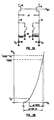
- Fig. 1 illustrates a type of static RAM memory cell which can be read at high speeds.
- the static RAM cell 10 has two pass transistors 30, 31 which are connected a first pair of complementary bit lines 72, 73.
- the gates of the NMOS transistors 30, 31 are connected to a word line 70.
- the two transistors 30, 31 are also connected to a latch 39 which is represented by two cross-coupled inverters 32, 33.
- the inverters contain complementary PMOS transistors to form a Complementary MOS circuit.
- These cross-coupled converters 32, 33 have two stable states, a "1" and a "0" logical state and thus can store the logical state for later access.
- This information is accessed or "read” by putting a high signal on the word line 70 so that the pass transistors 30, 31 are turned on so that the bit lines 72,73 are connected to the inverters 32, 33. During this read cycle the voltage of one of the bit lines remains high in its precharged state and the other goes low. This condition sets a sense amplifier into one state or another, which is connected to the bit lines 72, 73.
- the two pass transistors 30, 31 are turned on by a signal on the word line 70.
- the voltage on one of the bit lines 72, 73 is set high and the other set low to drive or "write” into the memory cell.
- the latch 39 formed by the inverters 32,33 is set into that logic state.
- the NMOS transistors 34, 36 are connected in series with the source electrode of the transistor 36 connected to ground and the drain electrode of the transistor 34 is connected to the bit line 74.
- the gate electrode of the transistor 36 is connected to the latch 39 of the memory cell, i.e., the output terminal of the inverter 32 and the input terminal of the second inverter 33.
- the gate electrode of the transistor 34 is connected to a second word line 71.
- the NMOS transistors 35, 37 are series-connected with the source electrode of the transistor 37 connected to ground and the drain electrode of the transistor 35 to the second bit line 75.
- the gate electrode of the transistor 37 is connected to the latch 39 of the memory cell, i.e., the output terminal of the inverter 33 and the input terminal of the second inverter 32.
- the gate electrode of the transistor 35 is connected to the second word line 71.
- a high-speed read operation is performed by turning on the transistors 34, 35 by a signal on the word line 71.
- the two bit lines 74, 75 are then respectively connected to the transistors 36, 37 which are, in turn, "on” or “off” in a complementary fashion.
- the state of the two transistors depends upon the information stored in the latch 39 of the memory cell. If the transistor 35 is on, then the bit line 74 is connected to ground and the transistor 37 is off so that the complementary bit line 75 is unconnected to ground. If the transistor 37 is on, then the bit line 75 is connected to ground instead. In this manner the bit lines 74, 75 provide for a faster access to the state of the memory cell.
- Fig. 2A is a generalized view of the memory cell and the bit lines 74, 75.
- the memory cell in Fig. 1 appears to be a pair of current sources 82, 83, one of which draws a current I SENSE when connected to its respective bit line 74,75.
- the current source 82 (comprising the transistors 34, 36) is coupled to the bit line 74, while the current source 83 (the transistors 35, 37) is coupled to the bit line 75.
- the signal of the word line 71 and the information stored in the latch 39 determines whether one of the current sources 82, 83 is switched on and which one.
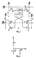
- Fig. 3 illustrates the present invention. Since the present invention is concerned with the high-speed read operation of the memory cells, Fig. 3 does not show the bit lines 72, 73 and the circuit related to the slower read and write operations of the memory cells, though it would be understood by those skilled in the art that such bit lines 72, 73 and related circuits exist in the complete integrated circuit device.
- the memory cell 10 is replicated in a grid-like array.
- a large number of memory cells is arranged vertically between the bit lines 74, 75 and each memory cell is connected to the bit lines.
- the column of memory cells is represented by the RAM core 85.
- One end of the bit line 74 is connected to a small current source represented by an MOS transistor 42, while the other end of the bit line is connected to a source electrode of an NMOS transistor 40.
- the complementary bit line 75 is similarly connected at one end to a small current source represented by a transistor 43 and at the other end to a source electrode of the NMOS transistor 41.
- the two NMOS transistors 40, 41 act as cascode transistors to isolate the large capacitances associated with each of the bit lines 74, 75 from the much smaller capacitances associated with the sensing circuitry coupled to the drain electrodes of transistors 40, 41. Without such isolation, the read operation of the one of the memory cells in the core 85 becomes much slower and cumbersome.
- the gate electrodes of the transistors 40, 41 are held at a reference voltage V REF , which ideally should be some interval from the supply voltage V CC , such as V CC /2. This allows some degree of freedom in the design of the sensing circuitry.
- a capacitor 89 is also connected to the gate electrodes of the transistors 40,41 to protect V REF from transients on the supply voltage at ground.
- Fig. 2A illustrates the transistors 42, 43 as current sources 80, 81 respectively.
- I CS small supply current
- Fig. 4 is a circuit diagram of the circuit used to generate the voltage on the gate electodes V CS of the transistors 42, 43.
- An NMOS transistor 87 and a resistor 86 are connected between the supply voltage (V CC is typically +5 volts) and ground.
- the transistor 87 is in a diode configation and thus has its gate electrode tied to its drain electrode. The source electrode is tied to ground.
- the value of the resistor 86 is hundreds of kiloohms so that a small current (actually I CS ) flows through the resistor and transistor.
- the gate electrodes of the transistors 42, 43 are connected to the gate electrode of the transistor 87 so that the transistors 42, 43 act as current mirrors of the current flowing through the transistor 87.
- the capacitor 88 acts as a cushion against fluctuations in the ground voltage.
- the present invention uses the change in currents, rather than voltages, through the bit lines 74, 75 as a memory cell in the core 80 is read. This provides for a much faster operation.
- the sense amplifier of the present invention has current mirrors connected to each of the drain electrodes of the transistors 40, 41.
- the drain electrode of the cascode transistor 40 is connected to the drain electrode to a diode-connected PMOS transistor 46, which when in operation provides the current, I CS or I CS +I SENSE , to the bit line.
- I CS is 8-20 microamperes
- I SENSE is 150-300 microamperes.
- the source electrode of the transistor 46 is connected to the V CC supply.
- a second PMOS transistor 48 has its source electrode connected to V CC and its gate electrode connected to the gate electrode of the transistor 46.
- the transistor 48 scaled up by a factor of 3, amplifies the current through the transistor 46.
- the current through the drain electrode of the transistor 48 is 3 times the current through the drain electrode of the transistor 46.
- PMOS transistors 47, 49 are connected to the drain electrode of the cascode transistor 41 which couples to the bit line 75.
- the drain electrode of the PMOS transistor 48 is connected to a drain and gate electrodes of a diode-connected NMOS transistor 60 having its source electrode connected to ground.
- the drain electrode of the PMOS transistor 49 is connected to the drain electrode of an NMOS transistor 61 which also has its source electrode connected to ground.
- the two transistors 60, 61 are the same size. Their gate electrodes connected together so that the NMOS transistor 61 tries to conduct as much current as the transistor 60 does.
- the transistor 49 is conducting the larger current and the transistor 48 the smaller, the transistor 61 in trying to follow the transistor 60 cannot accept the large current. Hence the node capacitance is charged and the node voltage goes high near to V CC . Then the transistor 49 goes into the linear mode and stops tracking the current through the transistor 47.
- An input terminal of an inverter 64 is connected to the node 63 formed by the drain electrodes of the transistors 49 and 61.
- the voltage on the node 63 can swing from near ground to near V CC , the slew rate may be slower than desired.
- the inverter 64 translates the voltage swings of the node 63 into full CMOS logic levels while isolating the node 63 from any additional capacitance associated with the output node of the inverter 64. Thus the completion of the sensing operation is accelerated.
- a further aspect is that typically static RAMs are laid out so that several columns of memory cells are laid out horizontally next to each other. As explained above, vertical bit line pairs are associated with each column. There are also horizontal word lines across the columns to access the memory cells in the columns so that a signal on a word line accesses memory cells in different columns.
- load devices are placed in the path of the currents on the bit lines to generate an output voltage differential for each bit line pair.
- Pass transistors are placed on the voltage output nodes associated with each line of the bit line pair.
- the pass transistors are connected in parallel to some output sense circuit.
- a multiplexer controller selects only one pair of pass transistors at a time so that only one column is accessed at a time. Thus only one memory cell in the columns is accessed at one time.
- Fig. 3 shows four columns of memory cells represented by RAM core 85 is connected to the active load transistors 60, 61 and the inverter 64.
- PMOS transistors 44, 45 Connected to the gate electrode of each PMOS transistor 46, 47 associated with each bit line pair 74, 75 are PMOS transistors 44, 45 which act as current switches. When turned on, these transistors 44, 45 steal current from the transistors 46, 47 so that these transistors 46, 47 do not conduct current.
- the gate electrode of each transistor 44, 45 is connected to the multiplexer control (not shown).
- the output signal from the multiplexer turns on that pair of transistors 44, 45.
- the transistors 46 and 47 are non-conducting and so are transistors 48 and 49.
- the transistors 44, 45 are turned off by the multiplexer control.
- the PMOS 46 and 47 become operational and the gained current mirror transistors 48, 49 are also operational.
- the selected column affects the voltage at the node 63.
- the transistors 44, 45 turn on and off simultaneously with the turn on of the transistors 34, 35 in the memory cell.
- the multiplexer selection is performed in parallel with the core memory cell. No additional delay is added in series with the sense path.
Landscapes
- Engineering & Computer Science (AREA)
- Microelectronics & Electronic Packaging (AREA)
- Computer Hardware Design (AREA)
- Static Random-Access Memory (AREA)
Applications Claiming Priority (2)
| Application Number | Priority Date | Filing Date | Title |
|---|---|---|---|
| US349564 | 1989-05-09 | ||
| US07/349,564 US5068830A (en) | 1989-05-09 | 1989-05-09 | High speed static ram sensing system |
Publications (2)
| Publication Number | Publication Date |
|---|---|
| EP0397355A2 true EP0397355A2 (de) | 1990-11-14 |
| EP0397355A3 EP0397355A3 (de) | 1991-01-30 |
Family
ID=23372945
Family Applications (1)
| Application Number | Title | Priority Date | Filing Date |
|---|---|---|---|
| EP19900304562 Withdrawn EP0397355A3 (de) | 1989-05-09 | 1990-04-26 | Stromgesteuerter Leseverstärker |
Country Status (2)
| Country | Link |
|---|---|
| US (1) | US5068830A (de) |
| EP (1) | EP0397355A3 (de) |
Cited By (4)
| Publication number | Priority date | Publication date | Assignee | Title |
|---|---|---|---|---|
| FR2749967A1 (fr) * | 1996-06-13 | 1997-12-19 | Sgs Thomson Microelectronics | Dispositif de lecture de cellules d'une memoire |
| WO2001018814A1 (en) * | 1999-08-24 | 2001-03-15 | Micron Technology, Inc. | Pseudo-differential current sense amplifier with hysteresis |
| US6307405B2 (en) | 1999-04-27 | 2001-10-23 | Micron Technology, Inc. | Current sense amplifier and current comparator with hysteresis |
| US6377084B2 (en) | 1999-02-22 | 2002-04-23 | Micron Technology, Inc. | Pseudo-differential amplifiers |
Families Citing this family (14)
| Publication number | Priority date | Publication date | Assignee | Title |
|---|---|---|---|---|
| JP2673395B2 (ja) * | 1990-08-29 | 1997-11-05 | 三菱電機株式会社 | 半導体記憶装置およびそのテスト方法 |
| US5293349A (en) * | 1991-06-24 | 1994-03-08 | Texas Instruments Incorporated | Memory cell circuits, devices, systems and methods of operation |
| US5258948A (en) * | 1992-02-03 | 1993-11-02 | Motorola, Inc. | Memory cell sense technique |
| JP3307473B2 (ja) * | 1992-09-09 | 2002-07-24 | ソニー エレクトロニクス インコーポレイテッド | 半導体メモリの試験回路 |
| US5377150A (en) * | 1993-03-31 | 1994-12-27 | Sgs-Thomson Microelectronics, Inc. | Disabling sense amplifier |
| JP3606951B2 (ja) * | 1995-06-26 | 2005-01-05 | 株式会社ルネサステクノロジ | 半導体記憶装置 |
| US5608681A (en) * | 1996-01-22 | 1997-03-04 | Lsi Logic Corporation | Fast memory sense system |
| US5844265A (en) * | 1996-07-11 | 1998-12-01 | Synaptics, Incorporated | Sense amplifier for high-density imaging array |
| EP1015872B1 (de) | 1996-12-12 | 2005-03-02 | Prolume, Ltd. | Vorrichtung und verfahren zum nachweis und identifizieren von infektiösen wirkstoffen |
| US8953395B2 (en) | 2012-02-23 | 2015-02-10 | Apple Inc. | Memory with variable strength sense amplifier |
| US9177671B2 (en) | 2012-02-23 | 2015-11-03 | Apple Inc. | Memory with bit line capacitive loading |
| US8780657B2 (en) | 2012-03-01 | 2014-07-15 | Apple Inc. | Memory with bit line current injection |
| US8559249B1 (en) | 2012-03-27 | 2013-10-15 | Apple Inc. | Memory with redundant sense amplifier |
| US8780654B2 (en) | 2012-04-10 | 2014-07-15 | Apple Inc. | Weak bit detection in a memory through variable development time |
Family Cites Families (4)
| Publication number | Priority date | Publication date | Assignee | Title |
|---|---|---|---|---|
| US4536859A (en) * | 1981-08-31 | 1985-08-20 | Sharp Kabushiki Kaisha | Cross-coupled inverters static random access memory |
| US4649301A (en) * | 1985-01-07 | 1987-03-10 | Thomson Components-Mostek Corp. | Multiple-input sense amplifier with two CMOS differential stages driving a high-gain stage |
| US4713797A (en) * | 1985-11-25 | 1987-12-15 | Motorola Inc. | Current mirror sense amplifier for a non-volatile memory |
| US4791324A (en) * | 1987-04-10 | 1988-12-13 | Motorola, Inc. | CMOS differential-amplifier sense amplifier |
-
1989
- 1989-05-09 US US07/349,564 patent/US5068830A/en not_active Expired - Lifetime
-
1990
- 1990-04-26 EP EP19900304562 patent/EP0397355A3/de not_active Withdrawn
Cited By (7)
| Publication number | Priority date | Publication date | Assignee | Title |
|---|---|---|---|---|
| FR2749967A1 (fr) * | 1996-06-13 | 1997-12-19 | Sgs Thomson Microelectronics | Dispositif de lecture de cellules d'une memoire |
| US5923590A (en) * | 1996-06-13 | 1999-07-13 | Sgs-Thomson Microelectronics S.A. | Device for reading cells of a memory |
| US6377084B2 (en) | 1999-02-22 | 2002-04-23 | Micron Technology, Inc. | Pseudo-differential amplifiers |
| US6307405B2 (en) | 1999-04-27 | 2001-10-23 | Micron Technology, Inc. | Current sense amplifier and current comparator with hysteresis |
| WO2001018814A1 (en) * | 1999-08-24 | 2001-03-15 | Micron Technology, Inc. | Pseudo-differential current sense amplifier with hysteresis |
| US6288575B1 (en) | 1999-08-24 | 2001-09-11 | Micron Technology, Inc. | Pseudo-differential current sense amplifier with hysteresis |
| US6538476B2 (en) | 1999-08-24 | 2003-03-25 | Micron Technology, Inc. | Method of forming a pseudo-differential current sense amplifier with hysteresis |
Also Published As
| Publication number | Publication date |
|---|---|
| EP0397355A3 (de) | 1991-01-30 |
| US5068830A (en) | 1991-11-26 |
Similar Documents
| Publication | Publication Date | Title |
|---|---|---|
| US5068830A (en) | High speed static ram sensing system | |
| US5371713A (en) | Semiconductor integrated circuit | |
| US4999519A (en) | Semiconductor circuit with low power consumption having emitter-coupled logic or differential amplifier | |
| US6154064A (en) | Differential sense amplifier circuit | |
| KR950000757B1 (ko) | 감지 증폭기를 갖는 반도체 메모리 | |
| US5046050A (en) | Shared BiCMOS sense amplifier | |
| US5226014A (en) | Low power pseudo-static ROM | |
| US5247479A (en) | Current sensing amplifier for SRAM | |
| EP0846326A1 (de) | Ladungsübertragungsabtastverstärker | |
| US5323349A (en) | Dynamic semiconductor memory device having separate read and write data bases | |
| US4785259A (en) | BIMOS memory sense amplifier system | |
| US5880990A (en) | Dual port memory apparatus operating a low voltage to maintain low operating current during charging and discharging | |
| KR20010070238A (ko) | 감소된 전력 소산으로 동작하는 sram | |
| US4903237A (en) | Differential sense amplifier circuit for high speed ROMS, and flash memory devices | |
| JP2756797B2 (ja) | Fetセンス・アンプ | |
| US5715204A (en) | Sense amplifier with hysteresis | |
| JP2760634B2 (ja) | 集積メモリ | |
| US7535782B2 (en) | Sense amplifier circuit and method for a DRAM | |
| EP0503524B1 (de) | Halbleiterspeicheranordnung | |
| US5083295A (en) | Integrated memory circuit with interconnected sense amplifiers | |
| JP2766056B2 (ja) | 電流センス増幅器 | |
| US5075891A (en) | Memory with a variable impedance bit line load circuit | |
| KR950006336B1 (ko) | 반도체 메모리장치의 전류센싱회로 | |
| US5646892A (en) | Data reading circuit | |
| KR20010088298A (ko) | 반도체 집적 회로 |
Legal Events
| Date | Code | Title | Description |
|---|---|---|---|
| PUAI | Public reference made under article 153(3) epc to a published international application that has entered the european phase |
Free format text: ORIGINAL CODE: 0009012 |
|
| AK | Designated contracting states |
Kind code of ref document: A2 Designated state(s): AT BE CH DE DK ES FR GB GR IT LI LU NL SE |
|
| PUAL | Search report despatched |
Free format text: ORIGINAL CODE: 0009013 |
|
| AK | Designated contracting states |
Kind code of ref document: A3 Designated state(s): AT BE CH DE DK ES FR GB GR IT LI LU NL SE |
|
| 17P | Request for examination filed |
Effective date: 19910502 |
|
| 17Q | First examination report despatched |
Effective date: 19931209 |
|
| STAA | Information on the status of an ep patent application or granted ep patent |
Free format text: STATUS: THE APPLICATION IS DEEMED TO BE WITHDRAWN |
|
| 18D | Application deemed to be withdrawn |
Effective date: 19950124 |