EP0392647A2 - Einrichtungen mit Frequenzumtastung für Stromschleife - Google Patents
Einrichtungen mit Frequenzumtastung für Stromschleife Download PDFInfo
- Publication number
- EP0392647A2 EP0392647A2 EP90300406A EP90300406A EP0392647A2 EP 0392647 A2 EP0392647 A2 EP 0392647A2 EP 90300406 A EP90300406 A EP 90300406A EP 90300406 A EP90300406 A EP 90300406A EP 0392647 A2 EP0392647 A2 EP 0392647A2
- Authority
- EP
- European Patent Office
- Prior art keywords
- current loop
- current
- frequency
- arrangement according
- demodulating
- Prior art date
- Legal status (The legal status is an assumption and is not a legal conclusion. Google has not performed a legal analysis and makes no representation as to the accuracy of the status listed.)
- Granted
Links
Images


Classifications
-
- H—ELECTRICITY
- H04—ELECTRIC COMMUNICATION TECHNIQUE
- H04L—TRANSMISSION OF DIGITAL INFORMATION, e.g. TELEGRAPHIC COMMUNICATION
- H04L27/00—Modulated-carrier systems
- H04L27/10—Frequency-modulated carrier systems, i.e. using frequency-shift keying
- H04L27/12—Modulator circuits; Transmitter circuits
-
- G—PHYSICS
- G08—SIGNALLING
- G08C—TRANSMISSION SYSTEMS FOR MEASURED VALUES, CONTROL OR SIMILAR SIGNALS
- G08C19/00—Electric signal transmission systems
- G08C19/02—Electric signal transmission systems in which the signal transmitted is magnitude of current or voltage
Definitions
- This invention relates to current loop arrangements.
- Frequency shift keying is a form of frequency modulation commonly used in low-speed modems in which two states of a signal are transmitted at two separate frequencies. A "1" is transmitted by a predefined signal frequency (space frequency) and a "0" is transmitted by another predefined signal frequency (mark frequency).
- FSK has more noise immunity than other forms of modulation, such as amplitude modulation or phase modulation.
- power limited devices such as loop transmitters and battery powered devices
- modulation techniques not utilising frequency shift keying have been developed, such as that employed in US Patent No. US-A-607 247 (Sterling, Jr., et al).
- a current loop arrangement having a power supply for supplying current at various current levels, a current loop connected to the power supply for carrying the current levels, modulating means for modulating frequency shift keying pulses to produce signals having a first predef ined frequency and a second predefined frequency, and connecting means for connecting the modulating means to the current loop, the connecting means permitting the communication of said signals produced by the modulating means onto the current loop.
- a current loop arrangement having a power supply for supplying a current at various current levels, a current loop connected to the power supply for carrying the current levels, said current levels being modulated by frequency shift keying pulses, demodulating means for demodulating said current level to produce frequency shift keying pulses, and connecting means for connecting the demodulating means to the current loop.
- the modulation system includes a digitally controlled oscillator whose output frequency is regulated by the rate of charging and discharging of a capacitor within the oscillator.
- a predefined upper frequency is determined by the value of a parallel combination of resistors, whereas a predefined lower frequency (space frequency) is determined by the ratio of the resistance of one of the foregoing resistors to the sum of the resistances of both resistors.
- the signal produced by the digitally controlled oscillator is superimposed on a current loop, enabling serial communication by FSK on the loop.
- the demodulation system includes a digitally controlled oscillator and a phase comparator interconnected in a phase-locked loop arrangement.
- the signal produced by the phase comparator is filtered and compared to another signal to produce an output signal that is a digital representation of the FSK superimposed on the current loop.
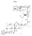
- FIG. 1 is a schematic diagram of a frequency shift keying modulation system 10.
- the system 10 comprises a transmitting interface device 12, a digitally controlled oscillator 14, a power supply 16 powering a current loop 18, and a circuit 20 interconnecting the digitally controlled oscillator 14 and the current loop 18.
- the interface device 12 is commonly referred to as an RS-232, or the like, and is properly referred to as an Interface Between Data Terminal Equipment and Data Communication Equipment Employing Serial Binary Data Interchange.
- the interface device 12 generates a supply voltage Vs for one of the two possible signal states (space frequency) and a zero output voltage for the other signal state (mark frequency).
- An output of the interface device 12 is connected (at a point F) to an input of an OR gate 30 within the digitally controlled oscillator 14.
- Another input of the OR gate 30 is connected at a point B to one side of a resistor 32 and to an input of an inverter 34.
- An output of the OR gate 30 is connected (at a point E) to a resistor 36 which is connected to the other side of the resistor 32 at a point A.
- An output of inverter 34 is connected at a point C to an input of an inverter 38 and to one side of a resistor 40.
- the other side of the resistor 40 is connected to the resistors 32 and 36 at the point A.
- a capacitor 42 is connected from the point A to an output of the inverter 38 (point D).
- the output of the inverter 38 which represents the output of the digitally controlled oscillator 14, is connected to an input of an inverter 44 in the circuit 20.
- An output of the inverter 44 is connected to a series combination of a resistor 46 and a capacitor 48 which is connected (at a point H) to one side of a transformer 50 which is grounded.
- the other side of the transformer 50 is connected across the current loop 18 via a resistor 52 and a capacitor 54.
- the current loop 18 includes a resistor 56 and is connected to an output of the power supply 16 that can typically draw a minimum of 4 mA to a maximum of 20 mA.
- the output voltage of the interface device 12 controls the frequency of the digitally controlled oscillator 14.
- the output of the interface device 12 is shown as a waveform F.
- the other waveforms shown in Figure 2 represent the voltages at various points within the modulation system 10 and correspond with the letters shown on Figure 1.
- presence of a supply voltage Vs at the output of the interface device 12 results in the digitally controlled oscillator 14 producing a predefined upper signal frequency (space frequency), whereas zero voltage at the output of the interface device 12 results in the oscillator 14 producing a predefined lower signal frequency (mark frequency).
- OR gate 30 acts as an inverter for the signal at the point B.
- the presence of a voltage at the point B, as shown in Figure 2 (position a), causes the voltages at the points E and C to be zero and the voltage at the point D to be the supply voltage Vs.
- the OR gate 30 and inverter 34 have high input impedances, a negligible current flows through the resistor 32 and the voltages at the points A and B are substantially equal to the supply voltage vs.
- the capacitor 42 starts charging from the point D through the resistors 40 and 36 to the points C and E, respectively, the voltage at the point A starts decreasing from the supply voltage Vs toward zero volts.
- the charging and discharging time of the capacitor 42 is proportional to the parallel combination of the resistors 40 and 36. Oscillations continue at the rate of charging and discharging of the capacitor 42, which represents the predefined upper signal frequency (space frequency), until the input voltage at the point F changes.
- the OR gate 30 When the output of the interface device 12 is zero volts ( Figure 2, position d), the OR gate 30 then acts as a non-inverting buffer for the voltage at the point B, resulting in the output at the point E equalling the input at the point B. This condition causes the points C and E to be of opposite potential at all times. When this occurs, the charging and discharging time of the capacitor 42 will be proportional to the ratio of the resistance of the resistor 40 to the sum of the resistances of the resistors 40 and 36. This results in the capacitor 42 charging and discharging at a slower rate which, in turn, causes oscillations to be produced at a predefined lower frequency (mark frequency).
- the digitally controlled oscillator 14 produces an output (at the point D) at a predefined upper signal frequency when the input voltage at the point F is equal to the supply voltage Vs and produces a predefined lower signal frequency when the input at the point F is zero volts.
- the output of the digitally controlled oscillator 14 drives the transformer 50 via the inverter 44, resistor 46 and capacitor 48.
- the transformer 50 is used to isolate the oscillator 14 from the current loop 18.
- the signal at the point H in Figure 1 is reflected to a point 1 by means of the transformer 50 and is ac-coupled to the current loop 18 through the resistor 52 and capacitor 54.
- the transformer 50 prevents any dc current from the current loop 18 from being transmitted to the digitally controlled oscillator 14, and vice versa. This permits on-line communication on the current loop 18 without disturbing the 4 to 20 mA dc current present thereon.
- FIG 3 is a schematic diagram of a frequency shift keying demodulation system 60. Those components in Figure 3 which are similar to the components utilised within the modulation system 10 shown in Figure 1 are designated by similar references and will not be discussed in further detail.
- the demodulation system 60 includes a demodulator 62, a circuit 64 interconnecting the demodulator 62 with the current loop 18, a digitally controlled oscillator 14, and a receiving interface device 66.
- the circuit 64 interconnects the current loop 18 with the demodulator 62 by means of a transformer 68 having one side connected across the current loop 18 via a resistor 70 and a capacitor 72.
- the other side of the transformer 68 is connected to ground and to a band-pass filter 74 having an output connected to one input of an OR gate 76 within the demodulator 62.
- Another input of the OR gate 76 is connected to the output of the inverter 38 within the digitally controlled oscillator 14.
- An output of the OR gate 76 is connected to an input of the OR gate 30 within the oscillator 14 and to a resistor 78 which is connected to one side of a resistor 80 and to ground via a capacitor 82.
- the other side of resistor 80 is connected to an input of an OR gate 84 and to an output of the OR gate 84 via a resistor 86.
- Another input of OR gate 84 is connected to ground.
- the output of the OR gate 84 is connected to the receiving interface device 66, which can be a RS-232, or the like.
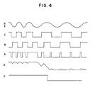
- Waveforms at selected points in Figure 3 are shown in Figure 4 and correspond with the letters shown in Figure 3.
- a frequency shift keying signal on the current loop 18 is transmitted through the capacitor 72, resistor 70 and transformer 68 to the band-pass filter 74.
- the ac-coupling of the transformer 68 prevents any dc current from the current loop 18 from passing to the demodulator 62.
- the band-pass filter 74 rejects any signal outside of the FSK band.
- the output of the filter 74 shown in Figure 4 as a waveform C, is a digital representation of the filtered FSK signal.
- the system constituted by the digitally controlled oscillator 14 and the OR gate 76 is a form of phase-locked loop.
- the signals at points B and C in Figure 3 are compared by the OR gate 76, producing an output at a point A in Figure 3 which is transmitted back to the digitally controlled oscillator 14 to adjust its frequency so as to be the same as the input frequency at the point C.
- the duty cycle of the digitally controlled oscillator 14 varies with the input frequency.
- a low input frequency produces an oscillator duty cycle of less than 50% whereas a high input frequency produces an oscillator duty cycle of greater than 50%.
- the signal at a point D in Figure 3 is the average of the signal produced at the point A filtered by the RC circuit constituted by the resistor 78 and capacitor 82.
- the OR gate 84 acts as a voltage comparator; i.e., if the voltage at the point D is above Vcc/2, then the voltage at a point F in Figure 3 goes high ( Figure 4-waveform F). However, if the voltage at the point D is less than Vcc/2, then the voltage at the point F goes low. In essence, the voltage at the point F is a digital representation of the FSK signal and can be transmitted to any data terminal equipment (not shown) by the interface device 66.
- the resistors 86 and 80 introduce a hysteresis to the OR gate 84 to reduce any jitter when a level transition occurs.
- modulation system 10 and the demodulation system 60 are their low power requirements. Such low power requirements can be attributed to the reduced number of components required within the systems, the use of CMOS chips where appropriate, and low unit values for the capacitors utilised.
- the systems 10 and 60 are also frequency stable under wide variations in power supply voltage because the input trip points (VIN and VIL) of the gates are proportional to the power supply voltage.
- the foregoing advantages permit reliable on-line communication between the low power devices using the same current loop that carried the 4 to 20 mA of dc without effecting the dc current value.
Applications Claiming Priority (2)
| Application Number | Priority Date | Filing Date | Title |
|---|---|---|---|
| US33700689A | 1989-04-12 | 1989-04-12 | |
| US337006 | 1989-04-12 |
Publications (3)
| Publication Number | Publication Date |
|---|---|
| EP0392647A2 true EP0392647A2 (de) | 1990-10-17 |
| EP0392647A3 EP0392647A3 (de) | 1991-01-09 |
| EP0392647B1 EP0392647B1 (de) | 1994-05-18 |
Family
ID=23318695
Family Applications (1)
| Application Number | Title | Priority Date | Filing Date |
|---|---|---|---|
| EP19900300406 Expired - Lifetime EP0392647B1 (de) | 1989-04-12 | 1990-01-15 | Einrichtungen mit Frequenzumtastung für Stromschleife |
Country Status (7)
| Country | Link |
|---|---|
| EP (1) | EP0392647B1 (de) |
| JP (1) | JPH02295258A (de) |
| CN (1) | CN1021182C (de) |
| AU (1) | AU628154B2 (de) |
| CA (1) | CA2013866A1 (de) |
| DE (1) | DE69008917T2 (de) |
| NO (1) | NO303259B1 (de) |
Cited By (4)
| Publication number | Priority date | Publication date | Assignee | Title |
|---|---|---|---|---|
| EP0487874A2 (de) * | 1990-11-30 | 1992-06-03 | Yokogawa Electric Corporation | Signalgestalter |
| DE29718405U1 (de) * | 1997-10-16 | 1998-11-12 | Siemens Ag | Analogeingabeeinheit |
| DE19813700A1 (de) * | 1998-03-27 | 1999-09-30 | Samson Ag | Eingangsschaltung für ein Feldgerät |
| CN104202076A (zh) * | 2014-08-21 | 2014-12-10 | 常州工学院 | 一种fsk中继器 |
Families Citing this family (6)
| Publication number | Priority date | Publication date | Assignee | Title |
|---|---|---|---|---|
| US5543447A (en) * | 1994-09-28 | 1996-08-06 | Southwest Research Institute | Stabilization of red amorphous phosphorus by ordered polymeric structures for the manufacture of non-emissive fire retardant plastics |
| IL125855A (en) * | 1998-04-06 | 2007-06-03 | Technion R & D Foundation Ltd | Method for the production of foamed ceramic materials |
| CN100336780C (zh) * | 2006-02-20 | 2007-09-12 | 河南科技大学 | 一种铸造用泡沫陶瓷过滤器的制备方法 |
| CN101043489B (zh) * | 2006-03-22 | 2012-07-04 | 普诚科技股份有限公司 | 频移键控解调电路、频率调制解调电路及其方法 |
| US8459525B2 (en) | 2008-02-14 | 2013-06-11 | Ethicon Endo-Sugery, Inc. | Motorized surgical cutting and fastening instrument having a magnetic drive train torque limiting device |
| DE102012218429A1 (de) | 2012-10-10 | 2014-04-10 | Zumtobel Lighting Gmbh | System zur Funktionsüberwachung einer Stromschleife |
Citations (4)
| Publication number | Priority date | Publication date | Assignee | Title |
|---|---|---|---|---|
| FR2342600A1 (fr) * | 1976-02-26 | 1977-09-23 | Vogelsang Remo | Systeme de transfert d'information |
| US4091361A (en) * | 1976-12-09 | 1978-05-23 | General Electric Company | Noise-immune carrier current actuated control |
| US4606049A (en) * | 1984-12-03 | 1986-08-12 | The United States Of America As Represented By The Secretary Of The Navy | Remote transmitter control system |
| GB2195798A (en) * | 1986-09-26 | 1988-04-13 | Endress Hauser Gmbh Co | Method and arrangement for transmitting binary-coded information in a measuring system |
Family Cites Families (5)
| Publication number | Priority date | Publication date | Assignee | Title |
|---|---|---|---|---|
| US3752923A (en) * | 1971-12-09 | 1973-08-14 | Honeywell Inf Systems | Frequency shift keyed generating system |
| JPS5493953A (en) * | 1978-01-07 | 1979-07-25 | Nec Corp | Frequency shift modulator circuit |
| JPS5827452A (ja) * | 1981-08-11 | 1983-02-18 | Mitsubishi Electric Corp | Fsk信号復調器 |
| JPS6174425A (ja) * | 1984-09-20 | 1986-04-16 | Matsushita Electric Ind Co Ltd | 電力線搬送送受信ネツトワ−クシステム |
| JPS648046U (de) * | 1987-07-02 | 1989-01-17 |
-
1990
- 1990-01-05 NO NO900046A patent/NO303259B1/no unknown
- 1990-01-15 DE DE1990608917 patent/DE69008917T2/de not_active Expired - Fee Related
- 1990-01-15 EP EP19900300406 patent/EP0392647B1/de not_active Expired - Lifetime
- 1990-03-03 CN CN 90101127 patent/CN1021182C/zh not_active Expired - Fee Related
- 1990-04-04 CA CA 2013866 patent/CA2013866A1/en not_active Abandoned
- 1990-04-11 JP JP2094207A patent/JPH02295258A/ja active Pending
- 1990-04-11 AU AU53170/90A patent/AU628154B2/en not_active Ceased
Patent Citations (4)
| Publication number | Priority date | Publication date | Assignee | Title |
|---|---|---|---|---|
| FR2342600A1 (fr) * | 1976-02-26 | 1977-09-23 | Vogelsang Remo | Systeme de transfert d'information |
| US4091361A (en) * | 1976-12-09 | 1978-05-23 | General Electric Company | Noise-immune carrier current actuated control |
| US4606049A (en) * | 1984-12-03 | 1986-08-12 | The United States Of America As Represented By The Secretary Of The Navy | Remote transmitter control system |
| GB2195798A (en) * | 1986-09-26 | 1988-04-13 | Endress Hauser Gmbh Co | Method and arrangement for transmitting binary-coded information in a measuring system |
Non-Patent Citations (1)
| Title |
|---|
| EDN ELECTRICAL DESIGN NEWS. vol. 27, no. 8, 14 April 1982, NEWTON, MASSACHUSETT page 196 R.RICE: "XOR gate controls oscillator frequency" * |
Cited By (6)
| Publication number | Priority date | Publication date | Assignee | Title |
|---|---|---|---|---|
| EP0487874A2 (de) * | 1990-11-30 | 1992-06-03 | Yokogawa Electric Corporation | Signalgestalter |
| EP0487874A3 (en) * | 1990-11-30 | 1993-06-09 | Yokogawa Electric Corporation | Signal conditioner |
| DE29718405U1 (de) * | 1997-10-16 | 1998-11-12 | Siemens Ag | Analogeingabeeinheit |
| DE19813700A1 (de) * | 1998-03-27 | 1999-09-30 | Samson Ag | Eingangsschaltung für ein Feldgerät |
| DE19813700C2 (de) * | 1998-03-27 | 2003-03-27 | Samson Ag | Eingangsschaltung für ein Feldgerät |
| CN104202076A (zh) * | 2014-08-21 | 2014-12-10 | 常州工学院 | 一种fsk中继器 |
Also Published As
| Publication number | Publication date |
|---|---|
| EP0392647B1 (de) | 1994-05-18 |
| AU5317090A (en) | 1990-10-18 |
| NO303259B1 (no) | 1998-06-15 |
| CN1046424A (zh) | 1990-10-24 |
| DE69008917T2 (de) | 1994-09-01 |
| CA2013866A1 (en) | 1990-10-12 |
| JPH02295258A (ja) | 1990-12-06 |
| CN1021182C (zh) | 1993-06-09 |
| NO900046D0 (no) | 1990-01-05 |
| NO900046L (no) | 1990-10-15 |
| DE69008917D1 (de) | 1994-06-23 |
| AU628154B2 (en) | 1992-09-10 |
| EP0392647A3 (de) | 1991-01-09 |
Similar Documents
| Publication | Publication Date | Title |
|---|---|---|
| US4497060A (en) | Self-clocking binary receiver | |
| US4417099A (en) | Electro-optical isolator circuit for line powered modem | |
| EP0392647A2 (de) | Einrichtungen mit Frequenzumtastung für Stromschleife | |
| US4368439A (en) | Frequency shift keying system | |
| US3986053A (en) | Regenerator for pulse code modulation systems | |
| US5438289A (en) | Comparator circuit | |
| US4399547A (en) | Receiver of pulsed phase modulated signals | |
| GB2148076A (en) | Microprocessor fsk data communications module | |
| JPH0257746B2 (de) | ||
| US6304043B1 (en) | Circuit arrangement for signal coupling between circuit parts having supply lines isolated from one another | |
| JPS58127451A (ja) | 発振器を周波数変調するための改良デ−タ回路 | |
| CA1284827C (en) | Demodulation circuit | |
| US4039952A (en) | Digital frequency shift-keyed transmitter | |
| US20020196065A1 (en) | Method and apparatus for generating pulses from analog waveforms | |
| US3506924A (en) | F.s.k. zero crossing detector | |
| US3637951A (en) | Recording head driver which avoids saturation | |
| US6486819B2 (en) | Circuitry with resistive input impedance for generating pulses from analog waveforms | |
| ATE28250T1 (de) | Schaltungsanordnung zur uebertragung von spannungssignalen. | |
| JP2754540B2 (ja) | パルスカウント型検波装置 | |
| KR940006354A (ko) | 주파수 변조(fm) 전송기의 전계 강도를 결정하는 장치가 있는 주파수 변조 수신기 | |
| KR900007550Y1 (ko) | 접지 분리형 데이타 전송회로 | |
| JP3367785B2 (ja) | 可変容量ダイオ−ドを使用した周波数変調回路装置 | |
| KR0178858B1 (ko) | 주파수 오차 및 위상 오차 검출 장치 | |
| KR910009846B1 (ko) | 드롭아웃 펄스 발생회로 | |
| KR920004375B1 (ko) | 고주파 수신장비의 노이즈 제거회로 |
Legal Events
| Date | Code | Title | Description |
|---|---|---|---|
| PUAI | Public reference made under article 153(3) epc to a published international application that has entered the european phase |
Free format text: ORIGINAL CODE: 0009012 |
|
| AK | Designated contracting states |
Kind code of ref document: A2 Designated state(s): DE FR GB IT |
|
| PUAL | Search report despatched |
Free format text: ORIGINAL CODE: 0009013 |
|
| RAP1 | Party data changed (applicant data changed or rights of an application transferred) |
Owner name: INTERNATIONAL CONTROL AUTOMATION FINANCE S.A. |
|
| AK | Designated contracting states |
Kind code of ref document: A3 Designated state(s): DE FR GB IT |
|
| 17P | Request for examination filed |
Effective date: 19901219 |
|
| 17Q | First examination report despatched |
Effective date: 19930301 |
|
| RTI1 | Title (correction) | ||
| GRAA | (expected) grant |
Free format text: ORIGINAL CODE: 0009210 |
|
| AK | Designated contracting states |
Kind code of ref document: B1 Designated state(s): DE FR GB IT |
|
| ITF | It: translation for a ep patent filed |
Owner name: MARIETTI E GISLON S.R.L. |
|
| REF | Corresponds to: |
Ref document number: 69008917 Country of ref document: DE Date of ref document: 19940623 |
|
| ET | Fr: translation filed | ||
| PLBE | No opposition filed within time limit |
Free format text: ORIGINAL CODE: 0009261 |
|
| STAA | Information on the status of an ep patent application or granted ep patent |
Free format text: STATUS: NO OPPOSITION FILED WITHIN TIME LIMIT |
|
| 26N | No opposition filed | ||
| PGFP | Annual fee paid to national office [announced via postgrant information from national office to epo] |
Ref country code: GB Payment date: 19991213 Year of fee payment: 11 |
|
| PGFP | Annual fee paid to national office [announced via postgrant information from national office to epo] |
Ref country code: DE Payment date: 19991217 Year of fee payment: 11 |
|
| PGFP | Annual fee paid to national office [announced via postgrant information from national office to epo] |
Ref country code: FR Payment date: 19991221 Year of fee payment: 11 |
|
| PG25 | Lapsed in a contracting state [announced via postgrant information from national office to epo] |
Ref country code: GB Free format text: LAPSE BECAUSE OF NON-PAYMENT OF DUE FEES Effective date: 20010115 |
|
| GBPC | Gb: european patent ceased through non-payment of renewal fee |
Effective date: 20010115 |
|
| PG25 | Lapsed in a contracting state [announced via postgrant information from national office to epo] |
Ref country code: FR Free format text: LAPSE BECAUSE OF NON-PAYMENT OF DUE FEES Effective date: 20010928 |
|
| PG25 | Lapsed in a contracting state [announced via postgrant information from national office to epo] |
Ref country code: DE Free format text: LAPSE BECAUSE OF NON-PAYMENT OF DUE FEES Effective date: 20011101 |
|
| REG | Reference to a national code |
Ref country code: FR Ref legal event code: ST |
|
| PG25 | Lapsed in a contracting state [announced via postgrant information from national office to epo] |
Ref country code: IT Free format text: LAPSE BECAUSE OF NON-PAYMENT OF DUE FEES Effective date: 20050115 |