EP0388441B1 - Verfahren und Vorrichtung für eine sichere und diagnostizierbare, Signalverwaschungen vermeidende Übertragung - Google Patents
Verfahren und Vorrichtung für eine sichere und diagnostizierbare, Signalverwaschungen vermeidende Übertragung Download PDFInfo
- Publication number
- EP0388441B1 EP0388441B1 EP89903545A EP89903545A EP0388441B1 EP 0388441 B1 EP0388441 B1 EP 0388441B1 EP 89903545 A EP89903545 A EP 89903545A EP 89903545 A EP89903545 A EP 89903545A EP 0388441 B1 EP0388441 B1 EP 0388441B1
- Authority
- EP
- European Patent Office
- Prior art keywords
- signal
- unit
- microprocessor
- request
- locked
- Prior art date
- Legal status (The legal status is an assumption and is not a legal conclusion. Google has not performed a legal analysis and makes no representation as to the accuracy of the status listed.)
- Expired - Lifetime
Links
- 238000004891 communication Methods 0.000 title claims abstract description 28
- 238000000034 method Methods 0.000 title claims description 10
- 230000005540 biological transmission Effects 0.000 claims abstract description 15
- 238000012360 testing method Methods 0.000 claims abstract description 14
- 230000007257 malfunction Effects 0.000 claims description 11
- 230000004044 response Effects 0.000 claims description 5
- 230000004913 activation Effects 0.000 claims description 2
- 230000008878 coupling Effects 0.000 claims description 2
- 238000010168 coupling process Methods 0.000 claims description 2
- 238000005859 coupling reaction Methods 0.000 claims description 2
- 238000010998 test method Methods 0.000 claims 5
- 230000001603 reducing effect Effects 0.000 claims 1
- 238000004886 process control Methods 0.000 description 10
- 238000010586 diagram Methods 0.000 description 3
- 230000009471 action Effects 0.000 description 2
- 230000008859 change Effects 0.000 description 2
- 230000000694 effects Effects 0.000 description 2
- 238000012545 processing Methods 0.000 description 2
- 238000012369 In process control Methods 0.000 description 1
- 230000009118 appropriate response Effects 0.000 description 1
- 230000001419 dependent effect Effects 0.000 description 1
- 238000013461 design Methods 0.000 description 1
- 238000001514 detection method Methods 0.000 description 1
- 230000003116 impacting effect Effects 0.000 description 1
- 238000010965 in-process control Methods 0.000 description 1
- 238000002955 isolation Methods 0.000 description 1
- 230000008569 process Effects 0.000 description 1
- 230000008054 signal transmission Effects 0.000 description 1
Images

Classifications
-
- H—ELECTRICITY
- H04—ELECTRIC COMMUNICATION TECHNIQUE
- H04L—TRANSMISSION OF DIGITAL INFORMATION, e.g. TELEGRAPHIC COMMUNICATION
- H04L43/00—Arrangements for monitoring or testing data switching networks
-
- H—ELECTRICITY
- H04—ELECTRIC COMMUNICATION TECHNIQUE
- H04L—TRANSMISSION OF DIGITAL INFORMATION, e.g. TELEGRAPHIC COMMUNICATION
- H04L43/00—Arrangements for monitoring or testing data switching networks
- H04L43/08—Monitoring or testing based on specific metrics, e.g. QoS, energy consumption or environmental parameters
- H04L43/0805—Monitoring or testing based on specific metrics, e.g. QoS, energy consumption or environmental parameters by checking availability
- H04L43/0817—Monitoring or testing based on specific metrics, e.g. QoS, energy consumption or environmental parameters by checking availability by checking functioning
Definitions
- This invention relates generally to networks that receive and transmit groups of logic signals from remote locations and, more particularly, to an apparatus for insuring the accuracy of the information transmitted between the local and the remote locations.
- Partyka describes a Fault-Tolerant Bus Transceiver System with means for eliminating jamming and RF interference.
- the system includes a multiloop structure in which each element is periodically and automatically tested and in which failure of any single component does not result in uncontrolled carrier transmission.
- the system allows for isolation and reporting of any single element failure before fatal multiple failure can occur.
- the system includes means and method steps as described in the preamble of the independent claims. Each time the microprocessor wants to send data, it has to perform certain relatively complex operations of toggling the two or more input signals of a sequencer, whose output is active in one and only one state.
- the sequencer can be just a counter. Acting more intelligently, the processor can make the sequencer to reach the state number N-1. Then only one change of the processor output port can activate the RF switch, and the next one would already disactivate it. The key idea is that the processor can access the RF switch only if it acts intelligently, precisely according to the program. Any random inputs to the sequencer are neglected. An additional level of security can be added by coupling the action of the sequencer with the action of two timers of which the first one is activated by the sequencer output.
- this timer When a prescribed time elapses and the output of the sequencer is still active, this timer resets the sequencer, thus even if the processor fails to change the sequencer state after transmitting a message, the RF switch is still turned off. Whenever a processor malfunction is detected either by a processor activity detector or by the first mentioned timer, then the second timer is activated and power is disconnected from the amplifier for a relatively long time by means of a supply voltage switch.
- process control networks are provided to collect status information by at least one central location and to distribute control signals to the devices coupled to the network.
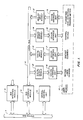
- the process control network includes a system bus 5 which has at least one central control unit 6 coupled thereto and at least one bus interface module 9 also coupled thereto.
- the central control unit 6 receives signals from the system bus 5 that typically communicate the status of user devices coupled to the process control network and applies signals to the network that provide the control signals determining the operation of the user devices.
- the bus interface unit 9 applies status signals to the system bus and receives signals from the system bus 5 which are relevant to a subset of network user devices 10 that communicate with the central control unit 6 through bus interface unit 9.
- User devices 10 providing digital status signals in response to contact closures provide status signals to the bus interface unit 9 by means of device interface unit 17 and digital input module 13.
- User devices 10 responding to analog control signals, such as control valves, receive signals from the bus interface unit 9 by means of output analog module 14 and device interface unit 18.
- User devices 10 of the type providing analog status information such as flowmeters, level detectors, pressure meters etc. provide the status signals to the bus interface unit through interface module 19 and analog input module 15.
- the device interface units 16, 17, 18 and 19 convert the signals received from and transmitted to the user devices into a format usable by the digital output and input modules and the analog output and input modules, respectively.
- the digital input and output modules 13 and 12 and the analog input and output modules 15 and 14 couple the signals of the user devices, as transformed by the device interface unit, with the bus interface unit 9 by means of local bus 11.
- the messages In the communication between the bus interface unit 9 and the digital and analog input and output devices, the messages typically have an upper bound on the time that a single message can be active (in the preferred embodiment, the upper limit is 10 milliseconds [ms]), however, this interval is a matter of design choice.
- a malfunction in the network can result in uncontrolled communication of information, generally referred to as jabber, in which the message can extend beyond the 10 ms boundary. Because the jabber is the result of a malfunction, such a condition must be detected and the network repaired or inactivated.
- the detection of a jabber event is typically performed by an antijabber timing unit which measures the length of the message.
- the antijabber circuit can itself malfunction and not detect a jabbering incident.
- a jabber incident can be the result of a single component malfunction.
- the invention further discloses a process control network having an antijabber circuit and having the capability of testing an antijabber timing circuit. Preferred details of the new method and embodiments of the new apparatus are described in the dependent claims.
- the aforementioned and other features are accomplished, according to the present invention, by providing a microprocessor unit with the capability of applying a timing signal to the antijabber timing unit.
- the timing signal has a duration longer than the maximum permitted message duration.
- a failure signal is transmitted to the microprocessor.
- the microprocessor will detect that no failure signal was received as a result of the timing signal and appropriate response can be taken.
- a signal is applied to the properly functioning antijabber to remove the failure signal and apparatus is provided to insure that the removal of the failure signal does not compromise the network communication.
- the antijabber circuit is also used to supply a second enable signal for the network to minimize the opportunity for a single component to result in a jabber event.
- Figure 1 is a block diagram of process control network capable of using the present invention.
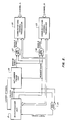
- Figure 2 is a block diagram of the principal components of the apparatus for testing an antijabber timing unit.
- Figure 3 is a timing diagram illustrating the relationship of the important signals used for testing the antijabber timing unit.
- Fig. 1 has been described with reference to the related art.
- Logic signal groups are exchanged between the microprocessor unit 21 and the communication channel transceivers 22 and 23 when the communications channel transceivers 22 or 23 are enabled.
- the microprocessor unit 21 applies an UNLOCK signal to antijabber timing unit 24 and to a second input terminal of logic 'AND' gate 25 and applies a REQUEST signal to the antijabber timing unit 24 and to a first terminal of logic 'AND' gate 27, to a first input terminal of logic 'AND' gate 26 and to a first terminal of logic 'AND' gate 25.
- the microprocessor receives a LOCKED-UP signal from antijabber timing unit 24 and a RESET signal from an output terminal of logic 'AND' gate 25.
- An output window signal from antijabber timing unit 24 is applied to a second input terminal of logic 'AND' gate 27 and to a second input terminal of logic 'AND' gate 26.
- the logic 'AND' gate 27 applies an ENABLE signal to communication channel transceiver 22 and logic 'AND' gate 26 applies an ENABLE signal to communication channel transceiver 23.
- Communication channel transceivers 22 and 23 exchange signal groups with the remainder of the process control network.
- a timing or REQUEST signal is generated by the microprocessor unit 21 and applied to antijabber timing unit 24.
- the antijabber timing unit After a period of time that exceeds the maximum period permitted for a message, the antijabber timing unit provides a LOCKED-UP signal indicating that the antijabber timing unit has detected a message that exceeds the maximum permitted length.
- the microprocessor applies an UNLOCK signal to the antijabber timing unit 24.
- the original REQUEST signal is inactivated prior to generation of the UNLOCK signal, a current REQUEST signal related to an actual message transmission can be present.
- the combination of a REQUEST signal and an UNLOCK signal causes the microprocessor to be reset by a RESET signal regardless of the state of the LOCKED-UP signal.
- the present invention makes use of the processing capability of a microprocessor unit used for transmission of messages over the network to provide a timing signal and determine if, as a result of the timing signal, the antijabber timing unit functioned correctly. Because the timing signal exceeds the maximum permitted message length, if a LOCKED-UP (failure) signal is not generated as a result of the timing signal, then the microprocessor unit responds to a antijabber timing unit malfunction. When a LOCKED-UP signal is generated by the antijabber timing unit, the microprocessor responds with an UNLOCK signal to the antijabber unit that inactivates the LOCKED-UP signal.
- a message request signal can be applied to the antijabber unit.
- the simultaneous presence of an UNLOCK signal and a message request signal results in the resetting of the microprocessor unit, i.e., any activity in progress will be aborted and reinitiated.
- the ENABLE signal for the communication channel transceiver 22 from logic 'AND' gate 27 and the ENABLE signal for the communication channel transceiver 23 from logic 'AND' gate 26 are activated by two signals, one from the microprocessor unit 21 and one (the WINDOW signal) from the antijabber timing unit.
- the WINDOW signal is present when the LOCKED-UP signal is not present, when a REQUEST signal is present and when the REQUEST signal has been active for less than the maximum signal transmission time.
Landscapes
- Engineering & Computer Science (AREA)
- Computer Networks & Wireless Communication (AREA)
- Signal Processing (AREA)
- Maintenance And Management Of Digital Transmission (AREA)
- Small-Scale Networks (AREA)
- Selective Calling Equipment (AREA)
- Mobile Radio Communication Systems (AREA)
- Telephone Function (AREA)
- Adornments (AREA)
- Cookers (AREA)
- Percussion Or Vibration Massage (AREA)
- Two-Way Televisions, Distribution Of Moving Picture Or The Like (AREA)
- Data Exchanges In Wide-Area Networks (AREA)
- Radar Systems Or Details Thereof (AREA)
- Polysaccharides And Polysaccharide Derivatives (AREA)
- Facsimile Transmission Control (AREA)
- Investigating Or Analyzing Materials By The Use Of Electric Means (AREA)
- Paper (AREA)
- Transmitters (AREA)
- Professional, Industrial, Or Sporting Protective Garments (AREA)
- Cultivation Receptacles Or Flower-Pots, Or Pots For Seedlings (AREA)
Claims (10)
- Einrichtung zum Verhindern unkontrollierter Kommunikation in einem Kommunikationsnetzwerk (22, 23) mita) einer ersten Einheit (21) zum Erzeugen eines ersten Signals (ANFORDERUNG), welches normalerweise die Übertragung von Datensignalen im Netzwerk bezeichnet;b) einer zweiten Einrichtung (24) mit einem an die erste Einheit angeschlossenen Zeitgeber zum Empfang des ersten Signals, welche auf das erste Signal anspricht und bei ordnungsgemäßem Betrieb ein zweites Signal (SPERRUNG) erzeugt, sobald das erste Signal eine vorgegebene Dauer überschreitet;
gekennzeichnet durchc) Mittel zum Ankoppeln des zweiten Signals an die erste Einheit (21), um dieser mitzuteilen, daß das erste Signal die vorgegebene Zeitdauer überschreitet;d) auf das zweite Signal ansprechende Mittel in der ersten Einheit (21), um ein drittes Signal (ENTSPERRUNG) zu erzeugen und der zweiten Einheit (24) zuzuführen; unde) auf das dritte Signal ansprechende Mittel in der zweiten Einheit (24), um das zweite Signal (SPERRUNG) zu beenden. - Einrichtung nach Anspruch 1, gekennzeichnet durcha) die Ausbildung der ersten Einheit (21) als Mikroprozessor und der zweiten Einheit (24) als Antiverwaschungs-Zeitgeber;b) Mittel im Mikroprozessor (21) zur Erzeugung des ersten Signals auch während eines Testvorgangs;c) auf das zweite Signal (SPERRUNG) ansprechende Mittel zum Verhindern der Übertragung von Datensignalen durch den Mikroprozessor (21) und zur Zufuhr des dritten Signals (ENTSPERRUNG) durch den Mikroprozessor an die Antiverwaschungs-Zeitgebereinheit (24), nachdem das erste Signal (ANFORDERUNG) während des Testvorgangs entfernt wurde, wobei das dritte Signal (ENTSPERRUNG) die Antiverwaschungs-Zeitgebereinheit (24) veranlaßt, das zweite Signal (SPERRUNG) zu beseitigen; undd) Mittel innerhalb des Mikroprozessors (21) zum Verhindern der Übertragung von Datensignalen, wenn das zweite Signal (SPERRUNG) nicht während des Testvorgangs erzeugt wird.
- Einrichtung nach Anspruch 2, gekennzeichnet durcha) ein auf eine gleichzeitige Anwesenheit des dritten Signals (ENTSPERRUNG) und des ersten Signals (ANFORDERUNG) ansprechendes Logikgatter (25) zur Erzeugung eines vierten Signals (RÜCKSTELLUNG); undb) Mittel zur Zufuhr des vierten Signals an den Mikroprozessor (21) sowie zum Anhalten des Betriebs des Mikroprozessors und zur Rücksetzung.
- Einrichtung nach einem der vorangehenden Ansprüche, gekennzeichnet durch zwischen den ersten (21) und zweiten (24) Einheiten einerseits und dem Kommunikationsnetzwerk (22, 23) andererseits angeordnete Isolierschaltungen (26, 27) zur Verringerung der Auswirkung eines Einzelkomponentenfehlers auf die Übertragung von Datensignalen über das Kommunikationsnetzwerk, in dem für jeden von mehreren Übertragungskanälen (22, 23) mehrere Aktivierungssignale erzeugt werden.
- Einrichtung nach Anspruch 4, dadurch gekennzeichnet, daß die Antriverwaschungs-Zeitgebereinheit (24) zwei Signaleinrichtungen zur Erzeugung eines fünften Signals (FENSTER) umfaßt, wenn das zweite Signal (SPERRUNG) nicht ansteht, und wobei das erste Signal (ANFORDERUNG) sowie das fünfte Signal (FENSTER) die Kommunikation vom Mikroprozessor (21) zum Kommunikationsnetzwerk (22, 23) aktivieren.
- Einrichtung nach einem der vorangehenden Ansprüche, gekennzeichnet durch eine Testeinrichtung zum Verifizieren des Betriebs der Antiverwaschungs-Zeitgebereinheit (24), wobei die Testeinrichtung erste Mittel innerhalb des Mikroprozessors (21) zum Erzeugen des ersten Signals (ANFORDERUNG) für eine Zeitspanne länger als die vorgegebene Zeitspanne während des Testvorgangs umfaßt, und wobei die Antiverwaschungs-Zeitgebereinheit (24) das zweite Signal (SPERRUNG) nach Ablauf der vorgegebenen Zeitspanne liefert; und durch zweite Mittel im Mikroprozessor (21) zum Identifizieren einer Fehlfunktion der Antiverwaschungs-Zeitgebereinheit, falls das zweite Signal (SPERRUNG) nicht während des Testvorgangs erzeugt wird.
- Verfahren zum Verhindern unkontrollierter Kommunikation über ein Kommunikationsnetzwerk mit den Schritten:a) Erzeugen eines ersten Signals (ANFORDERUNG), sobald ein Mikroprozessor (21) Datensignale an das Kommunikationsnetzwerk (22, 23) überträgt;b) Anlegen des ersten Signals (ANFORDERUNG) an eine Zeitgebereinheit; undc) Erzeugen eines zweiten Signals (SPERRUNG) durch die Zeitgebereinheit (24), wenn das den Datensignalen zugeordnete erste Signal (ANFORDERUNG) eine vorgegebene Zeitspanne überdauert;
gekennzeichnet durch die weiteren Schritte:d) Anlegen des zweiten Signals (SPERRUNG) an den Mikroprozessor, wobei das zweite Signal einen Verwaschungsvorgang anzeigt;e) periodisches Erzeugen eines ersten Testsignals (ANFORDERUNG), welches die vorgegebene Zeitspanne übersteigt und welches der Zeitgebereinheit (24) zugeleitet wird;f) Erzeugen eines dritten Signals (ENTSPERREN) durch den Mikroprozessor (21), sobald ein zweites Signal als Antwort auf das erste Testsignal empfangen wird, sowie Zufuhr des dritten Signals an die Zeitgebereinheit, wobei das zweite Signal in Beantwortung des dritten Signals beseitigt wird; undg) Verhindern der Übertragung von Datensignalen durch den Mikroprozessor (21) an das Kommuikationsnetzwerk, wenn das zweite Signal (SPERRUNG) nicht in Beantwortung des ersten Testsignals (ANFORDERUNG) erzeugt wird. - Verfahren nach Anspruch 7, gekennzeichnet durch den weiteren Schritt einer Wiederaktivierung der Übertragung von Datensignalen durch den Mikroprozessor (21), wenn das erste Testsignal (ANFORDERUNG) und das dritte Signal (ENTSPERRUNG) gleichzeitig anstehen.
- Verfahren nach Anspruch 7 oder 8, gekennzeichnet durch den weiteren Schritt der Erzeugung eines fünften Signals (FENSTER) durch die Zeitgebereinheit (24), sobald das zweite Signal (SPERRUNG) nicht vorhanden ist, und wobei das fünfte Signal (FENSTER) ein getrenntes Signal für die Aktivierung der Übertragung von Datensignalen an das Kommunikationsnetzwerk liefert.
- Verfahren nach Anspruch 7, 8 oder 9, dadurch gekennzeichnet, daß das erste Signal (ANFORDERUNG) ein Aktivierungssignal für die Zulassung der Übertragung von Datensignalen an das Kommunikationsnetzwerk (22, 23) ist.
Priority Applications (1)
| Application Number | Priority Date | Filing Date | Title |
|---|---|---|---|
| AT89903545T ATE91833T1 (de) | 1987-11-17 | 1988-11-16 | Verfahren und vorrichtung fuer eine sichere und diagnostizierbare, signalverwaschungen vermeidende uebertragung. |
Applications Claiming Priority (2)
| Application Number | Priority Date | Filing Date | Title |
|---|---|---|---|
| US121548 | 1987-11-17 | ||
| US07/121,548 US4860280A (en) | 1987-11-17 | 1987-11-17 | Apparatus and method for a secure and diagnosable antijabber communication circuit |
Publications (2)
| Publication Number | Publication Date |
|---|---|
| EP0388441A1 EP0388441A1 (de) | 1990-09-26 |
| EP0388441B1 true EP0388441B1 (de) | 1993-07-21 |
Family
ID=22397413
Family Applications (1)
| Application Number | Title | Priority Date | Filing Date |
|---|---|---|---|
| EP89903545A Expired - Lifetime EP0388441B1 (de) | 1987-11-17 | 1988-11-16 | Verfahren und Vorrichtung für eine sichere und diagnostizierbare, Signalverwaschungen vermeidende Übertragung |
Country Status (10)
| Country | Link |
|---|---|
| US (1) | US4860280A (de) |
| EP (1) | EP0388441B1 (de) |
| JP (1) | JPH0646737B2 (de) |
| AT (1) | ATE91833T1 (de) |
| AU (1) | AU617788B2 (de) |
| CA (1) | CA1331645C (de) |
| DE (1) | DE3882537T2 (de) |
| NO (1) | NO902115D0 (de) |
| SG (1) | SG111393G (de) |
| WO (1) | WO1989005076A2 (de) |
Families Citing this family (3)
| Publication number | Priority date | Publication date | Assignee | Title |
|---|---|---|---|---|
| US5272700A (en) * | 1989-02-28 | 1993-12-21 | First Pacific Networks, Inc. | Spectrally efficient broadband transmission system |
| US5870589A (en) * | 1997-07-23 | 1999-02-09 | International Business Machines Corporation | Method for enhanced broadcast and unknown server operation |
| GB2386804A (en) * | 2002-03-22 | 2003-09-24 | Motorola Inc | Communications network node access switches |
Family Cites Families (5)
| Publication number | Priority date | Publication date | Assignee | Title |
|---|---|---|---|---|
| US4613858A (en) * | 1983-10-28 | 1986-09-23 | Sperry Corporation | Error isolator for bi-directional communications buses |
| US4680581A (en) * | 1985-03-28 | 1987-07-14 | Honeywell Inc. | Local area network special function frames |
| US4701910A (en) * | 1985-11-29 | 1987-10-20 | General Electric Company | Reliable local area network including active stations |
| US4692919A (en) * | 1985-11-29 | 1987-09-08 | Scientific Atlanta, Inc. | Communications network |
| US4700344A (en) * | 1986-06-13 | 1987-10-13 | Ncr Corporation | Processor overrun circuit |
-
1987
- 1987-11-17 US US07/121,548 patent/US4860280A/en not_active Expired - Lifetime
-
1988
- 1988-11-16 EP EP89903545A patent/EP0388441B1/de not_active Expired - Lifetime
- 1988-11-16 AT AT89903545T patent/ATE91833T1/de not_active IP Right Cessation
- 1988-11-16 DE DE89903545T patent/DE3882537T2/de not_active Expired - Fee Related
- 1988-11-16 AU AU32857/89A patent/AU617788B2/en not_active Ceased
- 1988-11-16 WO PCT/US1988/004100 patent/WO1989005076A2/en not_active Ceased
- 1988-11-16 JP JP1503258A patent/JPH0646737B2/ja not_active Expired - Lifetime
- 1988-11-17 CA CA000583335A patent/CA1331645C/en not_active Expired - Fee Related
-
1990
- 1990-05-11 NO NO902115A patent/NO902115D0/no unknown
-
1993
- 1993-10-02 SG SG111393A patent/SG111393G/en unknown
Also Published As
| Publication number | Publication date |
|---|---|
| CA1331645C (en) | 1994-08-23 |
| NO902115L (no) | 1990-05-11 |
| AU3285789A (en) | 1989-06-14 |
| EP0388441A1 (de) | 1990-09-26 |
| SG111393G (en) | 1994-02-25 |
| NO902115D0 (no) | 1990-05-11 |
| WO1989005076A3 (en) | 1989-07-27 |
| WO1989005076A2 (en) | 1989-06-01 |
| DE3882537T2 (de) | 1993-12-16 |
| DE3882537D1 (de) | 1993-08-26 |
| JPH0646737B2 (ja) | 1994-06-15 |
| JPH03502035A (ja) | 1991-05-09 |
| US4860280A (en) | 1989-08-22 |
| ATE91833T1 (de) | 1993-08-15 |
| AU617788B2 (en) | 1991-12-05 |
Similar Documents
| Publication | Publication Date | Title |
|---|---|---|
| JP2726315B2 (ja) | 移動通信システムの回線異常検出方法 | |
| US5406248A (en) | Method and apparatus for managing information transmissions on an electrical distribution circuit | |
| US4860280A (en) | Apparatus and method for a secure and diagnosable antijabber communication circuit | |
| US6528901B1 (en) | Automatic protection switching | |
| JP2618890B2 (ja) | 異常送信検出方式 | |
| JPS6351617B2 (de) | ||
| KR0174669B1 (ko) | 셉트 전송장비에서 장애 검출장치 | |
| JP2988127B2 (ja) | 通信制御装置 | |
| JPH0716194B2 (ja) | モニタ方式 | |
| JPH05327737A (ja) | 通信異常監視装置 | |
| JP2661102B2 (ja) | データ伝送装置 | |
| JPS6314542B2 (de) | ||
| JP3261876B2 (ja) | 光伝送路断線検出装置 | |
| JPH0716193B2 (ja) | 変復調装置のパワ−オフ検出方式 | |
| JPS6051999A (ja) | 警報試験方式 | |
| JPH0735470Y2 (ja) | ループ式データ伝送装置 | |
| JPH0318378B2 (de) | ||
| JPH09181753A (ja) | データ処理装置の異常検出装置 | |
| JPS61285315A (ja) | 遠隔制御型燃焼制御装置 | |
| JPS6122494B2 (de) | ||
| JPS616934A (ja) | 予備システム監視方式 | |
| JPS60106233A (ja) | 伝送路切替装置 | |
| JPS5941623B2 (ja) | 回線監視方式 | |
| JP2000124936A (ja) | 遠隔運用システム | |
| JPS6086947A (ja) | 遠隔監視制御装置におけるボ−リング方式 |
Legal Events
| Date | Code | Title | Description |
|---|---|---|---|
| PUAI | Public reference made under article 153(3) epc to a published international application that has entered the european phase |
Free format text: ORIGINAL CODE: 0009012 |
|
| 17P | Request for examination filed |
Effective date: 19900510 |
|
| AK | Designated contracting states |
Kind code of ref document: A1 Designated state(s): AT BE CH DE FR GB IT LI LU NL SE |
|
| 17Q | First examination report despatched |
Effective date: 19920722 |
|
| GRAA | (expected) grant |
Free format text: ORIGINAL CODE: 0009210 |
|
| AK | Designated contracting states |
Kind code of ref document: B1 Designated state(s): AT BE CH DE FR GB IT LI LU NL SE |
|
| REF | Corresponds to: |
Ref document number: 91833 Country of ref document: AT Date of ref document: 19930815 Kind code of ref document: T |
|
| REF | Corresponds to: |
Ref document number: 3882537 Country of ref document: DE Date of ref document: 19930826 |
|
| ET | Fr: translation filed | ||
| ITF | It: translation for a ep patent filed | ||
| EPTA | Lu: last paid annual fee | ||
| PLBE | No opposition filed within time limit |
Free format text: ORIGINAL CODE: 0009261 |
|
| STAA | Information on the status of an ep patent application or granted ep patent |
Free format text: STATUS: NO OPPOSITION FILED WITHIN TIME LIMIT |
|
| 26N | No opposition filed | ||
| PGFP | Annual fee paid to national office [announced via postgrant information from national office to epo] |
Ref country code: SE Payment date: 19940919 Year of fee payment: 7 |
|
| PGFP | Annual fee paid to national office [announced via postgrant information from national office to epo] |
Ref country code: GB Payment date: 19940920 Year of fee payment: 7 |
|
| PGFP | Annual fee paid to national office [announced via postgrant information from national office to epo] |
Ref country code: LU Payment date: 19941001 Year of fee payment: 7 |
|
| PGFP | Annual fee paid to national office [announced via postgrant information from national office to epo] |
Ref country code: AT Payment date: 19941004 Year of fee payment: 7 |
|
| PGFP | Annual fee paid to national office [announced via postgrant information from national office to epo] |
Ref country code: BE Payment date: 19941027 Year of fee payment: 7 |
|
| PGFP | Annual fee paid to national office [announced via postgrant information from national office to epo] |
Ref country code: NL Payment date: 19941130 Year of fee payment: 7 |
|
| EAL | Se: european patent in force in sweden |
Ref document number: 89903545.5 |
|
| PG25 | Lapsed in a contracting state [announced via postgrant information from national office to epo] |
Ref country code: LU Free format text: LAPSE BECAUSE OF NON-PAYMENT OF DUE FEES Effective date: 19951116 Ref country code: GB Effective date: 19951116 Ref country code: AT Effective date: 19951116 |
|
| PG25 | Lapsed in a contracting state [announced via postgrant information from national office to epo] |
Ref country code: SE Effective date: 19951117 |
|
| PG25 | Lapsed in a contracting state [announced via postgrant information from national office to epo] |
Ref country code: BE Effective date: 19951130 |
|
| BERE | Be: lapsed |
Owner name: HONEYWELL INC. Effective date: 19951130 |
|
| PG25 | Lapsed in a contracting state [announced via postgrant information from national office to epo] |
Ref country code: NL Effective date: 19960601 |
|
| GBPC | Gb: european patent ceased through non-payment of renewal fee |
Effective date: 19951116 |
|
| NLV4 | Nl: lapsed or anulled due to non-payment of the annual fee |
Effective date: 19960601 |
|
| EUG | Se: european patent has lapsed |
Ref document number: 89903545.5 |
|
| PGFP | Annual fee paid to national office [announced via postgrant information from national office to epo] |
Ref country code: FR Payment date: 20051104 Year of fee payment: 18 |
|
| PG25 | Lapsed in a contracting state [announced via postgrant information from national office to epo] |
Ref country code: IT Free format text: LAPSE BECAUSE OF NON-PAYMENT OF DUE FEES Effective date: 20051116 |
|
| PGFP | Annual fee paid to national office [announced via postgrant information from national office to epo] |
Ref country code: DE Payment date: 20051130 Year of fee payment: 18 |
|
| PGFP | Annual fee paid to national office [announced via postgrant information from national office to epo] |
Ref country code: CH Payment date: 20051216 Year of fee payment: 18 |
|
| PG25 | Lapsed in a contracting state [announced via postgrant information from national office to epo] |
Ref country code: LI Free format text: LAPSE BECAUSE OF NON-PAYMENT OF DUE FEES Effective date: 20061130 Ref country code: CH Free format text: LAPSE BECAUSE OF NON-PAYMENT OF DUE FEES Effective date: 20061130 |
|
| PG25 | Lapsed in a contracting state [announced via postgrant information from national office to epo] |
Ref country code: DE Free format text: LAPSE BECAUSE OF NON-PAYMENT OF DUE FEES Effective date: 20070601 |
|
| REG | Reference to a national code |
Ref country code: CH Ref legal event code: PL |
|
| REG | Reference to a national code |
Ref country code: FR Ref legal event code: ST Effective date: 20070731 |
|
| PG25 | Lapsed in a contracting state [announced via postgrant information from national office to epo] |
Ref country code: FR Free format text: LAPSE BECAUSE OF NON-PAYMENT OF DUE FEES Effective date: 20061130 |