EP0387010A2 - Bipolarer Transistor mit Heteroübergang - Google Patents
Bipolarer Transistor mit Heteroübergang Download PDFInfo
- Publication number
- EP0387010A2 EP0387010A2 EP90302391A EP90302391A EP0387010A2 EP 0387010 A2 EP0387010 A2 EP 0387010A2 EP 90302391 A EP90302391 A EP 90302391A EP 90302391 A EP90302391 A EP 90302391A EP 0387010 A2 EP0387010 A2 EP 0387010A2
- Authority
- EP
- European Patent Office
- Prior art keywords
- layer
- base
- emitter
- type
- electrode
- Prior art date
- Legal status (The legal status is an assumption and is not a legal conclusion. Google has not performed a legal analysis and makes no representation as to the accuracy of the status listed.)
- Withdrawn
Links
Images


Classifications
-
- H—ELECTRICITY
- H10—SEMICONDUCTOR DEVICES; ELECTRIC SOLID-STATE DEVICES NOT OTHERWISE PROVIDED FOR
- H10D—INORGANIC ELECTRIC SEMICONDUCTOR DEVICES
- H10D10/00—Bipolar junction transistors [BJT]
- H10D10/01—Manufacture or treatment
- H10D10/021—Manufacture or treatment of heterojunction BJTs [HBT]
-
- H—ELECTRICITY
- H10—SEMICONDUCTOR DEVICES; ELECTRIC SOLID-STATE DEVICES NOT OTHERWISE PROVIDED FOR
- H10D—INORGANIC ELECTRIC SEMICONDUCTOR DEVICES
- H10D10/00—Bipolar junction transistors [BJT]
- H10D10/80—Heterojunction BJTs
- H10D10/821—Vertical heterojunction BJTs
-
- H—ELECTRICITY
- H10—SEMICONDUCTOR DEVICES; ELECTRIC SOLID-STATE DEVICES NOT OTHERWISE PROVIDED FOR
- H10D—INORGANIC ELECTRIC SEMICONDUCTOR DEVICES
- H10D64/00—Electrodes of devices having potential barriers
- H10D64/01—Manufacture or treatment
- H10D64/011—Manufacture or treatment of electrodes ohmically coupled to a semiconductor
-
- H—ELECTRICITY
- H10—SEMICONDUCTOR DEVICES; ELECTRIC SOLID-STATE DEVICES NOT OTHERWISE PROVIDED FOR
- H10D—INORGANIC ELECTRIC SEMICONDUCTOR DEVICES
- H10D62/00—Semiconductor bodies, or regions thereof, of devices having potential barriers
- H10D62/80—Semiconductor bodies, or regions thereof, of devices having potential barriers characterised by the materials
- H10D62/82—Heterojunctions
- H10D62/824—Heterojunctions comprising only Group III-V materials heterojunctions, e.g. GaN/AlGaN heterojunctions
-
- H—ELECTRICITY
- H10—SEMICONDUCTOR DEVICES; ELECTRIC SOLID-STATE DEVICES NOT OTHERWISE PROVIDED FOR
- H10D—INORGANIC ELECTRIC SEMICONDUCTOR DEVICES
- H10D62/00—Semiconductor bodies, or regions thereof, of devices having potential barriers
- H10D62/80—Semiconductor bodies, or regions thereof, of devices having potential barriers characterised by the materials
- H10D62/85—Semiconductor bodies, or regions thereof, of devices having potential barriers characterised by the materials being Group III-V materials, e.g. GaAs
- H10D62/852—Semiconductor bodies, or regions thereof, of devices having potential barriers characterised by the materials being Group III-V materials, e.g. GaAs being Group III-V materials comprising three or more elements, e.g. AlGaN or InAsSbP
Definitions
- the present invention relates to a hetero-junction bipolar transistor (HBT) which is promising as a super high speed, super high frequency device.
- HBT hetero-junction bipolar transistor
- HBT a semiconductor material having the larger energy band gap than the base is used as an emitter. Accordingly, a reverse injection from the base to the emitter is suppressed, and the injection efficiency of the carrier from the emitter to the base is enlarged. For this reason, different from an ordinary homo-junction bipolar transistor, the emitter can be formed into low dope and the base into high dope state. As this permits to reduce the base resistance, it is advantageous to make the maximum oscillation frequency Fm large. Further, as it is possible to make the base thinner and greatly shorten the base running time of minority carriers injected from the emitter and reduce the junction capacitance between the emitter and the base, HBT is essentially advantageous for enlarging the current gain cut-off frequency Ft. For these reasons, HBT is vigorously studied and developed as a super high frequency device.
- the base surface between the mesa of the emitter cap layer and the base electrode is covered with the depleted wide band gap emitter layer which is in epitaxial relation to each other, the defects dependent on surface dungling bonds are decreased, and as the potential of the energy conduction band of the depleted emitter layer is higher than that of the base layer, the surface recombination is remarkably reduced, thereby making it possible to prevent the lowering of ⁇ .
- this structure for formation of a base electrode having small contact resistance, elimination of depleted emitter layer is indispensable, so that it is impossible to suppress the electrons which reach the base electrode. Accordingly, this structure is not much effective for the self-alignment type HBT for reducing the base resistance.
- An object of the present invention is to keep the current gain large by suppressing the surface recombination over the whole area of the external base of a hetero-junction bipolar transistor (HBT) and to render the base resistance small.
- HBT hetero-junction bipolar transistor
- the HBT of the present invention has, as a surface protective film layer, an epitaxially formed p-type semiconductor layer which has the higher portential of the energy conduction band than that of the base layer on an external base layer outside the junction between the mesa of the n-type emitter layer and the p-type base layer, and has a base electrode thereon.
- the HBT has, on the p-type surface protective layer a p-type semiconouctor layer which shows a smaller contact resistance with the base electrode. More preferably, a base electrode is formed adjacent to the emitter.
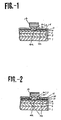
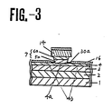
- Fig. 1, Fig 2, and Fig. 3 are the sectional views showing the embodiment of the structure of HBT according to the present invention.
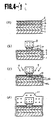
- Fig. 4, Fig. 5, and Fig. 6 are the sectional views showing the embodiments of the method of producing the HBT according to the present invention.
- each number denotes the following:
- GaAs substrate S, I, GaAs
- 2 ... n-type highly doped GaAs (n+-GaAs), 3 ... n-type doped GaAs (n-GaAs), 4 ... p-type highly doped GaAs (p+-GaAs), 4a ... intrinsic base part comprising 4, 4b ... external base part comprising the layer 4, 5 ... n-type doped Al 0 ⁇ 3 Ga 0 ⁇ 7 As (n-Al 0 ⁇ 3 Ga 0 ⁇ 7 As), 5a ... layer of 5 constituting an emitter mesa, 6 ... n-type highly doped GaAs (n+-GaAs), 6a ...
- p-type highly doped GaAs p+-GaAs
- the first embodiment of the HBT structure of the present invention is shown in Fig. 1.
- Fig. 1 there is shown a relation between the emitter and the base which is an essential condition of the present invention.
- This HBT structure has a semi-insulating GaAs (S.I.- GaAs) 1, an n-type highly doped GaAs (n+-GaAs) layer 2 for forming a collector contact layer, a collector layer 3 comprising an n-type doped GaAs (n-GaAs), a base layer 4 comprising a p-type highly doped GaAs (p+-GaAs), an emitter mesa 7 comprising a wide band gap Al 0 ⁇ 3 Ga 0 ⁇ 7 As(n-Al 0 ⁇ 3 Ga 0 ⁇ 7 As) emitter layer 5a which is n-type doped thereon and n+-GaAs 6a, an emitter electrode 14 covering the emitter mesa 7 in an umbrella shape, a p-type highly
- this HBT structure a part of the electrons injected from the emitter to the intrinsic base part 4a joined to the emitter mesa 7 diffuses in the direction of the external base 4b, but, as the potential of the energy conduction band of the p+-Al 0 ⁇ 4 Ga 0 ⁇ 6 As layer 10 which is epitaxially formed on the external base 4b is higher than that of the base layer 4, these diffused electrons are reflected by this barrier and do not appear to the surface. Accordingly, this HBT shows extremely small surface recombination which is in general a problematic point in the AlGaAs/GaAs type HBT. Also, because the layer 10 is of a highly doped p-type, a base electrode can be formed thereon.
- the HBT of this structure is extremely effective for preparing an HBT having small base resistance and large current gain.
- n-Al 0 ⁇ 3 Ga 0 ⁇ 7 As as an emitter layer 5 and p+-GaAs as a base layer 4.
- materials to satisfy the essential conditions of HBT there may be used n-Al 0 ⁇ 3 Ga 0 ⁇ 7 As as an emitter and p+-Al Y Ga 1-Y As (Y being fixed or varied; Y ⁇ X) having the smaller band gap than the former as a base.
- p-Al 0 ⁇ 4 Ga 0 ⁇ 6 As is used, which is in order to make the potential of the energy conduction band higher than p+- GaAs.
- p+-Al Z Ga 1-Z As Z > Y
- the intrinsic base is p+-Al Y Ga 1-Y As.
- Ga(Sb, As) type material may be used.
- HBT comprising AlGaAs/GaAs material
- HBT comprising other material may be similarly formed into the HBT structure of the present invention.
- the base electrode 16 exists adjacent to the emitter mesa in contact with the projection part of the emitter electrode 14 to the p+-Al 0 ⁇ 4 Ga 0 ⁇ 6 As layer 10. This state is formed by the production process of the present structure. This is because of the reduction of the component of the base resistance dependent on the distance between the emitter mesa and the base electrode so as to increase Fm. However, in order to increase Ft, the base electrode is not necessarily required to be formed in adjacent relation.
- Fig. 4 shows the process for production thereof.
- n+-GaAs layer 2 On S.I.-GaAs substrate, there are formed n+-GaAs layer 2, n-GaAs layer 3, p+-GaAs layer 4, n-Al 0 ⁇ 3 Ga 0 ⁇ 2 As layer 5, and n+-GaAs layer 6 in this order to prepare a multi-layer structure material by using molecular beam epitaxy (MBE) [Fig.
- MBE molecular beam epitaxy
- SiO2 is formed over the whole surface; SiO2 mask (dummy emitter) 8 is formed on a portion to be an emitter; and an emitter mesa 7 comprising n-Al 0 ⁇ 3 Ga 0 ⁇ 7 As 5a and n+-GaAs 6a is formed by wet-etching using the dummy emitter 8 to expose a base layer 4 [Fig. 4(b)].
- a p+-Al 0 ⁇ 4 Ga 0 ⁇ 6 As 10 is formed on the external base 4b by MBE [Fig. 4(c)].
- the surface is rendered flat by spin coating with a photoresist 11 [Fig. 4(d)].
- the resist is etched by dry etching to expose the head of the dummy emitter 8 [Fig. 4(e)]. Then, SiO2 dummy emitter 8 is eliminated by HF to form an opening 13 of the resist to which the top surface of the emitter mesa 7 is exposed [Fig. 4(f)]. From the upper part AuGe/Ni/Au is vapor deposited as an emitter electrode, and lifted off to form an emitter electrode 14 [Fig. 4(g)]. Then, using the emitter electrode 14 as a mask, a base electrode 16 comprising Cr/AuZn/Au is formed by vapor deposition process [Fig. 4(h)].
- an emitter electrode can be readily formed on an emitter mesa.
- a protective layer which is capable of suppressing a surface recombination is epitaxially formed, and on it a base electrode can be formed adjacent to the emitter mesa by a self-alignment method.
- SiO2 is used as a dummy emitter, but SiN X may be used.
- the base electrode 16 is formed by self-alignment against the emitter mesa 7.
- the base electrode 16 is formed by self-alignment, followed by forming an emitter by inverting a dummy emitter 8 into an emitter.
- MBE process is employed for forming the p+-Al 0 ⁇ 4 Ga 0 ⁇ 6 As layer, but any other epitaxy process such as metal-organic chemical vapor deposition (MO-CVD) may be used.
- MO-CVD metal-organic chemical vapor deposition
- Fig 2 is a second embodiment of the structure of HBT of the present invention.
- the point of difference of this embodiment from the first embodiment is that a high dope p+-GaAs is formed as a material for reducing the contact resistance with the base electrode 16 between the epitaxially formed p+-Al 0 ⁇ 4 Ga 0 ⁇ 6 As layer 10 and the base electrode 16.
- the second embodiment shows a structure of HBT which can not only suppress an increase of the base contact resistnce in the case where the surface protective layer of the external base induces an increase in the base contact resistance but also can realize further reduction of the base contact resistance even when such increase is not induced. in the structure of Fig.
- the base contact resistance in p+-GaAs, can be rendered smaller than in p+-Al 0 ⁇ 4 Ga 0 ⁇ 6 As, so that it has a characteristic of being capable of reducing the base resistance further than in the case of Fig. 1.
- the concentration of the carrier of the base layer 4 cannot be so high so as to prevent undesirable effect on diffusion of dopant to the upper and lower layers existing in contact therewith and on epitaxy formation of the upper layer of the base layer, reduction of the base contact resistance is limited. In this structure, however, as it is possible to render the carrier concentration of the p+-GaAs layer 20 for base contact formation extremely large, the base contact resistance can be rendered sufficiently small.
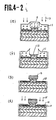
- FIG. 5 shows the process for production thereof.
- a surface protective film layer 10 is formed [Fig. 5(a)]
- a base contact layer 20 is formed by MBE 17 from the upper part [Fig. 5(b)]
- the dummy emitter 8 is inverted to the emitter electrode 14 [Fig. 5 from (c) to (f)].
- a base electrode 16 is formed by self-alignment adjacent to the emitter mesa 7 [Fig. 5(g)].
- the third embodiment of the present invention is shown in Fig. 3.
- the points of the difference of this embodiment from the first and second embodiments are that the surface protective film layer 30a of the p+-GaAs external base 4b is positioned between the base electrode 16 which exists in contact with the projection part of the emitter electrode 14 to the external base 4b and the emitter mesa 7, the surface protective film layer 30a is epitaxially formed on the external base 4b, and it is formed of a material in which the potential of its energy conduction band is higher than that of the base.
- the base resistance is reduced, and as the surface protective film of the externai base surface between the base electrode 16 and the emitter mesa 7 has the higher energy conduction band potential than the base, the surface recombination of this portion is suppressed, so that the lowering of current gain by surface recombination can be prevented.
- this structure shows the smaller effect of reduction of the current gain than the embodiments 1 and 2.
- p+-Al 0 ⁇ 4 Ga 0 ⁇ 6 As is used as a surface protective film 30a, but it may be an insulating materiai if the potential of the energy conduction band is higher than that of the base.
- FIG. 6 shows a process for production of this structure.
- Fig. 4(b) by an oblique direction MBE 9, p+-Al 0 ⁇ 4 Ga 0 ⁇ 6 As 30 is epitaxially formed on the external base 4b [Fig. 6(a)], and then, using the processes similar to Fig. 4(d) to (g) [Fig. 6 (b) to (e)], the dummy emitter 8 is inverted to the emitter electode 14 [Fig. 6(e)].
- an anisotropic dry etching 18 is applied from the upper part to etch the p+-Al Z Ga 1-Z A layer 30 to form a surface protectrive film layer 30a only on the lower part of the emitter electrode 14 [Fig. 6(f)].
- a base electrode 16 is formed by self-alignment process by metal vapor deposition 15 from the upper part [Fig. 6(g)].
Landscapes
- Bipolar Transistors (AREA)
Applications Claiming Priority (4)
| Application Number | Priority Date | Filing Date | Title |
|---|---|---|---|
| JP1056846A JPH02235340A (ja) | 1989-03-08 | 1989-03-08 | ヘテロ接合バイポーラトランジスタおよびその製造方法 |
| JP1056849A JPH02235343A (ja) | 1989-03-08 | 1989-03-08 | ヘテロ接合バイポーラトランジスタおよびその製造方法 |
| JP56849/89 | 1989-03-08 | ||
| JP56846/89 | 1989-03-08 |
Publications (2)
| Publication Number | Publication Date |
|---|---|
| EP0387010A2 true EP0387010A2 (de) | 1990-09-12 |
| EP0387010A3 EP0387010A3 (de) | 1990-10-10 |
Family
ID=26397836
Family Applications (1)
| Application Number | Title | Priority Date | Filing Date |
|---|---|---|---|
| EP19900302391 Withdrawn EP0387010A3 (de) | 1989-03-08 | 1990-03-06 | Bipolarer Transistor mit Heteroübergang |
Country Status (1)
| Country | Link |
|---|---|
| EP (1) | EP0387010A3 (de) |
Cited By (2)
| Publication number | Priority date | Publication date | Assignee | Title |
|---|---|---|---|---|
| US5296733A (en) * | 1989-11-27 | 1994-03-22 | Hitachi, Ltd. | Hetero junction bipolar transistor with improved electrode wiring contact region |
| FR2804247A1 (fr) * | 2000-01-21 | 2001-07-27 | St Microelectronics Sa | Procede de realisation d'un transistor bipolaire a emetteur et base extrinseque auto-alignes |
Citations (1)
| Publication number | Priority date | Publication date | Assignee | Title |
|---|---|---|---|---|
| JPS61193294A (ja) | 1985-02-20 | 1986-08-27 | 東芝機器株式会社 | 自動販売装置 |
Family Cites Families (4)
| Publication number | Priority date | Publication date | Assignee | Title |
|---|---|---|---|---|
| US4380774A (en) * | 1980-12-19 | 1983-04-19 | The United States Of America As Represented By The Secretary Of The Navy | High-performance bipolar microwave transistor |
| JPS61198776A (ja) * | 1985-02-28 | 1986-09-03 | Fujitsu Ltd | ヘテロ接合バイポ−ラトランジスタおよびその製造方法 |
| EP0240307B1 (de) * | 1986-04-01 | 1993-12-22 | Matsushita Electric Industrial Co., Ltd. | Bipolarer Transistor und sein Herstellungsverfahren |
| JPH0797589B2 (ja) * | 1986-06-26 | 1995-10-18 | ソニー株式会社 | ヘテロ接合型バイポ−ラトランジスタの製造方法 |
-
1990
- 1990-03-06 EP EP19900302391 patent/EP0387010A3/de not_active Withdrawn
Patent Citations (1)
| Publication number | Priority date | Publication date | Assignee | Title |
|---|---|---|---|---|
| JPS61193294A (ja) | 1985-02-20 | 1986-08-27 | 東芝機器株式会社 | 自動販売装置 |
Non-Patent Citations (3)
| Title |
|---|
| C. J. SANDROFF ET AL., APPL. PHYS. LETT., vol. 51, 1987, pages 33 - 35 |
| NOTTENBURG ET AL., APPL. PHYS. LETT., vol. 52, 1989, pages 218 - 220 |
| W. E. LEE ET AL., IEEE ELECTRON DEVICE LETT., vol. EDL-10, 1989, pages 202 - 202 |
Cited By (3)
| Publication number | Priority date | Publication date | Assignee | Title |
|---|---|---|---|---|
| US5296733A (en) * | 1989-11-27 | 1994-03-22 | Hitachi, Ltd. | Hetero junction bipolar transistor with improved electrode wiring contact region |
| FR2804247A1 (fr) * | 2000-01-21 | 2001-07-27 | St Microelectronics Sa | Procede de realisation d'un transistor bipolaire a emetteur et base extrinseque auto-alignes |
| US6465317B2 (en) | 2000-01-21 | 2002-10-15 | Stmicroelectronics S.A. | Process for producing a bipolar transistor with self-aligned emitter and extrinsic base |
Also Published As
| Publication number | Publication date |
|---|---|
| EP0387010A3 (de) | 1990-10-10 |
Similar Documents
| Publication | Publication Date | Title |
|---|---|---|
| US5166081A (en) | Method of producing a bipolar transistor | |
| US5525818A (en) | Reducing extrinsic base-collector capacitance | |
| US5903018A (en) | Bipolar transistor including a compound semiconductor | |
| US5298439A (en) | 1/f noise reduction in heterojunction bipolar transistors | |
| JPH0797589B2 (ja) | ヘテロ接合型バイポ−ラトランジスタの製造方法 | |
| US6462362B1 (en) | Heterojunction bipolar transistor having prevention layer between base and emitter | |
| US6825508B2 (en) | Heterojunction bipolar transistor and production process therefor | |
| US20040016941A1 (en) | Hetero-junction bipolar transistor and a manufacturing method of the same | |
| US4644381A (en) | I2 L heterostructure bipolar transistors and method of making the same | |
| EP0335720B1 (de) | Bipolartransistor und Verfahren zu seiner Herstellung | |
| EP0387010A2 (de) | Bipolarer Transistor mit Heteroübergang | |
| JPH05136159A (ja) | ヘテロ接合型バイポーラトランジスタ及びその製造方法 | |
| US6492664B2 (en) | Heterojunction bipolar transistor with reduced offset voltage | |
| US5153692A (en) | Semiconductor device | |
| JP4092597B2 (ja) | 半導体装置及びその製造方法 | |
| JP2623655B2 (ja) | バイポーラトランジスタおよびその製造方法 | |
| JPH09246281A (ja) | ヘテロ接合バイポーラトランジスタ | |
| US11211480B2 (en) | Heterojunction bipolar transistor | |
| JP3624357B2 (ja) | ヘテロ接合バイポーラトランジスタの製造方法 | |
| JP2615983B2 (ja) | ヘテロ接合バイポーラトランジスタの製造方法 | |
| KR100319738B1 (ko) | 동일한오믹금속을전극으로갖는이종접합쌍극자트랜지스터제조방법 | |
| KR100352375B1 (ko) | 이종접합 쌍극자 트랜지스터의 제조방법 | |
| JPS6381977A (ja) | ヘテロ接合バイポ−ラトランジスタ | |
| JP2841380B2 (ja) | ヘテロ接合バイポーラトランジスタ | |
| JP2976664B2 (ja) | バイポーラトランジスタの製造方法 |
Legal Events
| Date | Code | Title | Description |
|---|---|---|---|
| PUAI | Public reference made under article 153(3) epc to a published international application that has entered the european phase |
Free format text: ORIGINAL CODE: 0009012 |
|
| PUAL | Search report despatched |
Free format text: ORIGINAL CODE: 0009013 |
|
| AK | Designated contracting states |
Kind code of ref document: A2 Designated state(s): DE FR GB NL |
|
| AK | Designated contracting states |
Kind code of ref document: A3 Designated state(s): DE FR GB NL |
|
| 17P | Request for examination filed |
Effective date: 19910325 |
|
| 17Q | First examination report despatched |
Effective date: 19940727 |
|
| STAA | Information on the status of an ep patent application or granted ep patent |
Free format text: STATUS: THE APPLICATION IS DEEMED TO BE WITHDRAWN |
|
| 18D | Application deemed to be withdrawn |
Effective date: 19941207 |