EP0382465A1 - Circuit de commande d'une tête d'impression par points à fils - Google Patents
Circuit de commande d'une tête d'impression par points à fils Download PDFInfo
- Publication number
- EP0382465A1 EP0382465A1 EP90301211A EP90301211A EP0382465A1 EP 0382465 A1 EP0382465 A1 EP 0382465A1 EP 90301211 A EP90301211 A EP 90301211A EP 90301211 A EP90301211 A EP 90301211A EP 0382465 A1 EP0382465 A1 EP 0382465A1
- Authority
- EP
- European Patent Office
- Prior art keywords
- circuit
- lever
- print head
- drive
- Prior art date
- Legal status (The legal status is an assumption and is not a legal conclusion. Google has not performed a legal analysis and makes no representation as to the accuracy of the status listed.)
- Granted
Links
Images


Classifications
-
- B—PERFORMING OPERATIONS; TRANSPORTING
- B41—PRINTING; LINING MACHINES; TYPEWRITERS; STAMPS
- B41J—TYPEWRITERS; SELECTIVE PRINTING MECHANISMS, i.e. MECHANISMS PRINTING OTHERWISE THAN FROM A FORME; CORRECTION OF TYPOGRAPHICAL ERRORS
- B41J2/00—Typewriters or selective printing mechanisms characterised by the printing or marking process for which they are designed
- B41J2/22—Typewriters or selective printing mechanisms characterised by the printing or marking process for which they are designed characterised by selective application of impact or pressure on a printing material or impression-transfer material
- B41J2/23—Typewriters or selective printing mechanisms characterised by the printing or marking process for which they are designed characterised by selective application of impact or pressure on a printing material or impression-transfer material using print wires
- B41J2/30—Control circuits for actuators
-
- B—PERFORMING OPERATIONS; TRANSPORTING
- B41—PRINTING; LINING MACHINES; TYPEWRITERS; STAMPS
- B41J—TYPEWRITERS; SELECTIVE PRINTING MECHANISMS, i.e. MECHANISMS PRINTING OTHERWISE THAN FROM A FORME; CORRECTION OF TYPOGRAPHICAL ERRORS
- B41J9/00—Hammer-impression mechanisms
- B41J9/44—Control for hammer-impression mechanisms
- B41J9/50—Control for hammer-impression mechanisms for compensating for the variations of printer drive conditions, e.g. for compensating for the variation of temperature or current supply
-
- B—PERFORMING OPERATIONS; TRANSPORTING
- B65—CONVEYING; PACKING; STORING; HANDLING THIN OR FILAMENTARY MATERIAL
- B65D—CONTAINERS FOR STORAGE OR TRANSPORT OF ARTICLES OR MATERIALS, e.g. BAGS, BARRELS, BOTTLES, BOXES, CANS, CARTONS, CRATES, DRUMS, JARS, TANKS, HOPPERS, FORWARDING CONTAINERS; ACCESSORIES, CLOSURES, OR FITTINGS THEREFOR; PACKAGING ELEMENTS; PACKAGES
- B65D47/00—Closures with filling and discharging, or with discharging, devices
- B65D47/04—Closures with discharging devices other than pumps
- B65D47/06—Closures with discharging devices other than pumps with pouring spouts or tubes; with discharge nozzles or passages
- B65D47/061—Closures with discharging devices other than pumps with pouring spouts or tubes; with discharge nozzles or passages with telescopic, retractable or reversible spouts, tubes or nozzles
- B65D47/063—Closures with discharging devices other than pumps with pouring spouts or tubes; with discharge nozzles or passages with telescopic, retractable or reversible spouts, tubes or nozzles with flexible parts
-
- B—PERFORMING OPERATIONS; TRANSPORTING
- B65—CONVEYING; PACKING; STORING; HANDLING THIN OR FILAMENTARY MATERIAL
- B65D—CONTAINERS FOR STORAGE OR TRANSPORT OF ARTICLES OR MATERIALS, e.g. BAGS, BARRELS, BOTTLES, BOXES, CANS, CARTONS, CRATES, DRUMS, JARS, TANKS, HOPPERS, FORWARDING CONTAINERS; ACCESSORIES, CLOSURES, OR FITTINGS THEREFOR; PACKAGING ELEMENTS; PACKAGES
- B65D47/00—Closures with filling and discharging, or with discharging, devices
- B65D47/04—Closures with discharging devices other than pumps
- B65D47/06—Closures with discharging devices other than pumps with pouring spouts or tubes; with discharge nozzles or passages
- B65D47/10—Closures with discharging devices other than pumps with pouring spouts or tubes; with discharge nozzles or passages having frangible closures
- B65D47/103—Membranes with a tearing element
-
- B—PERFORMING OPERATIONS; TRANSPORTING
- B65—CONVEYING; PACKING; STORING; HANDLING THIN OR FILAMENTARY MATERIAL
- B65D—CONTAINERS FOR STORAGE OR TRANSPORT OF ARTICLES OR MATERIALS, e.g. BAGS, BARRELS, BOTTLES, BOXES, CANS, CARTONS, CRATES, DRUMS, JARS, TANKS, HOPPERS, FORWARDING CONTAINERS; ACCESSORIES, CLOSURES, OR FITTINGS THEREFOR; PACKAGING ELEMENTS; PACKAGES
- B65D47/00—Closures with filling and discharging, or with discharging, devices
- B65D47/04—Closures with discharging devices other than pumps
- B65D47/06—Closures with discharging devices other than pumps with pouring spouts or tubes; with discharge nozzles or passages
- B65D47/12—Closures with discharging devices other than pumps with pouring spouts or tubes; with discharge nozzles or passages having removable closures
- B65D47/127—Snap-on caps
- B65D47/128—Snap-on caps with internal parts
Definitions
- This invention relates to drive circuits for driving wire dot print heads which are adapted to print characters, figures, etc. in the form of a group of dots.
- a print wire strikes a platen under the action of the magnetic attractive force of an electro-magnetic coil to perform printing. After printing, the print wire and its associated lever are repulsed by the platen and returned to an initial position or, alternatively, are returned by a return spring.
- the print head is provided with a damper member made of a high visco-elasticity material such as rubber in order to stop rebounding when the print wire returns to the initial position.
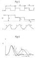
- Such a damper member can sufficiently damp the rebounding of the print wire at room temperature, so that the combination of the print wire and its associated lever together can be stopped in the initial position (see the solid curve 2 in Figure 6).
- JP-A-61-222761 and JP-A-63-317370 have proposed the provision of re-energising the electro-magnetic coil for a short period after the completion of printing to cancel any excessive return force returning the print wire to the initial position.
- the present invention seeks to provide a drive circuit for driving a wire dot print head, which circuit can return each print wire properly to an initial position irrespective of the temperature of the print head, thereby to prevent undesired movement of the print wires and permitting high speed printing.
- a drive circuit for driving a wire dot print head including a driving coil, a lever for causing a print wire to strike a platen under the action of the driving coil, a spring member for urging the lever to an initial position, and a damper member for absorbing kinetic energy of the lever when it returns to the initial position, characterised by comprising circuit means for causing current to flow through the driving coil when the lever is returning to the initial position when the temperature of the print head is outside a set temperature range, so that, in operation, a braking force is applied to the lever.
- the circuit means comprises a DC drive power circuit connected to one end of the driving coil, a switching means connected to the other end of the driving coil, and an output gate whose output is connected to the switching means one of whose input terminals is connected to receive a print data signal and the other of whose input terminals is connected to receive a signal from a reference timing signal generating means.
- the reference timing signal generating means may be composed of a drive pulse signal generating circuit arranged to be actuated by a print timing pulse to deliver a pulse having a given period to drive the lever and a braking pulse signal generating means arranged to deliver, when the temperature of the print head is outside the set temperature range, a pulse having a pre-determined interval during the return of the lever to the initial position.
- the circuit means comprises a DC drive power circuit connected to one end of the driving coil, a switching means connected to the other end of the driving coil, the switching means being arranged to be turned on/off in response to a print data signal, a diode reverse connected with respect to the DC drive power circuit, and a spark suppression circuit connected between the DC drive power circuit and, through the diode, the drive coil, the arrangement being such that, in operation, the conduction potential of the spark suppression circuit is controlled in response to the temperature of the print head.
- the spark suppression circuit may include a plurality of diodes forward connected with respect to the DC drive power circuit, one or more of said diodes being short-circuited when the temperature of the print head is outside the set temperature range.
- the drive circuit may include temperature sensitive means for sensing the temperature of the print head.
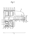
- FIG. 1 shows one embodiment of a wire dot print head 4 driven by a drive circuit according to the present invention.
- the print head 4 is capable of high dot density printing and includes two head units 20, 21 fixed to a nose member 22 in superposed arrangement.
- respective cup-shaped casings 23, 24 made of magnetic material and serving as a core, are formed with core portions 17 equi-distantly arranged in the circumferential direction.
- Each core portion 17 is provided with a driving coil 5.
- a lever 6 is rotatably supported via a pin 25 fixed to the respective casings 23, 24.
- Each lever 6 has a print wire 7 fixed thereto, the print wires being guided in the nose member 22.
- a return spring 12 is provided for urging the print wire 7 in a direction away from a platen 16.
- a damper member 13 made of rubber or other resilient material is provided on the side of the spring 12 opposite the platen so that the lever 6 lies between the damper member 13 and the spring 12.
- the damper member 13 is arranged to absorb any impulse arising when the lever 6, having performed a printing operation, returns to an initial position (shown in Figure 1) under the action of the return spring 12 thereby preventing a rebounding of the lever 6.
- a temperature sensor 8, such as a thermistor, is provided for detecting the temperature of the print head to deliver a temperature signal.
- the temperature sensor 8 is accommodated inside the casing 23 as illustrated.
- a terminal board 9 is provided for connection of the driving coil 5 to an external circuit.
- a guide board 10 guides the print wires 7.
- the lever 6 In the print head 4, when a driving pulse is supplied to the driving coil 5, the lever 6 is attracted by the magnetic force of the driving coil 5 against the biasing force of the spring 12, so that the print wire 7 moves towards the platen 16. As a result, the print wire 7 strikes an ink ribbon 11 and printing paper 15 lying between the platen 16 and the print head 4 to create a dot on the printing paper 15.
- the driving pulse is terminated after a given period, the lever 6 is moved back to the initial position by the spring 12, and any resulting impulse is absorbed by the damper member 13 so that the lever 6 stops at the initial position.
- FIG 2 shows a drive circuit according to the present invention for driving the print head 4 shown in Figure 1.
- Each driving coil 5 is connected at one end to a DC drive power circuit 30 and at the other end to ground through a switching transistor 32, and a spark suppression circuit is connected across each driving coil.
- Each spark suppression circuit is a series combination of a reverse connected diode 34 and a forward connected voltage regulation diode 36, the connections being with respect to the DC power circuit 30.
- each switching transistor 32 is connected to a corresponding output of an output circuit 42 consisting of a plurality of AND gates 40.
- Each AND gate 40 has one input terminal connected to receive a print data signal D and its other input terminal connected to receive a signal from a reference timing signal generating circuit 50.
- the reference timing signal generating circuit 50 consists of a drive pulse signal generating circuit 51, an AND gate 52, an interval setting circuit 53, a brake pulse signal generating circuit 54, and an OR gate 55.
- the drive pulse signal generating circuit 51 is adapted, upon receipt of a printing timing pulse A, to deliver a drive pulse signal C of, for example, 230 micro-seconds, this period being necessary to drive the print wire 7.
- the AND gate 52 receives the drive pulse signal C at one input terminal and its other input terminal receives a signal B from a temperature detecting circuit 56.
- the AND gate 52 produces an output when a high level signal (hereinafter referred to as "an H-level signal”) is supplied from the temperature detecting circuit 56.
- the interval setting circuit 53 has set therein an interval T1 of, for example, 60 micro-seconds, this interval corresponding to the time necessary for the print wire 7 to return to the initial position using the print timing pulse A as a reference point.
- the brake pulse signal generating circuit 54 is actuated at the time a pulse signal E from the interval setting circuit 53 falls thereby to deliver a brake pulse signal F of interval T2.
- This interval T2 is set to, for example, 50 micro-seconds in order that the lever 6 and the print wire 7, having returned to the initial position, can be satisfactorily decelerated to such an extent that there is no rebound even when the temperature of the print head 4, or the temperature of the damper member 13, is outside a set temperature range.
- the output terminals of the drive pulse signal generating circuit 51 and the brake pulse signal generating circuit 54 are connected to respective input terminals of the OR gate 55 whose output is connected to the input terminal of the output circuit 42.
- the temperature detecting circuit 56 is a window comparator which receives a signal from the temperature sensor 8 for detecting the temperature of the print head and delivers a low level signal (hereinafter referred to as "a L-level signal") when the detected temperature is within the set temperature range of, for example, 5°C to 70°C or an H-level signal when it is outside the set temperature range.
- a L-level signal a low level signal
- the drive pulse signal generating circuit 51 delivers the drive pulse signal C which, after passing through the OR gate 55, acts to open the AND gate 40 of the output circuit 12.
- the print data signal D for selection of a print wire to be driven is delivered in timed relation to the delivery of the print timing pulse.
- the respective AND gate 40 of the print wire which has to perform a printing operation delivers a pulse synchronised to the drive pulse signal C to turn ON the switching transistor 32 connected to the AND gate 40, so that current is supplied from the DC drive power circuit 30 to the driving coil 5.
- the driving coil 5 is energised to attract the lever 6, so that the print wire 7 is moved towards the platen 16.
- the drive pulse signal C is applied to the AND gate 52 but, since the temperature of the print head 4 is within the set temperature range, the temperature detecting circuit 56 is delivering a L-level signal, hence, the AND gate 52 delivers no H-level signal that is output. Consequently, the interval setting circuit 53 and the brake pulse signal generating circuit 54 are in a non-operating state.
- the print wire 7 strikes the platen 16 and is returned by the lever 6 under the action of the return spring 12 and when it reaches the initial position the resulting impulse is absorbed by the damper member 13 and so it comes to rest.
- the temperature detecting circuit 56 delivers an H-level signal B.
- the drive pulse signal generating circuit 51 delivers the drive pulse signal C.
- a current I a is caused to flow through the driving coil 5 as in the case where the temperature of the print head is within the set temperature range, so that the print wire 7 strikes the platen 16.
- the drive pulse C After passing through the AND gate 52, which is in the open state due to the H-level signal from the temperature detecting circuit 56, the drive pulse C is applied to the interval setting circuit 53, so that the latter is actuated.
- the brake pulse signal generating circuit 54 delivers the brake pulse signal F.
- the switching transistor 32 relating to the print wire 7 that has just performed a printing operation is again turned ON by the brake pulse signal F from the AND gate 40.
- a current I c is caused to flow from the DC drive power circuit 30 through the driving coil 5, thereby energising the latter. Consequently, the lever 6 as it returns to the initial position is attracted by the driving coil 5 in opposition to the action of the return spring 12 and contacts the damper member 13 while being damped (see the one-dot chain curve 3 in Figure 6).
- the brake pulse signal F is applied only when the temperature of the print head is higher than the upper limit of the set temperature range, the rebound of the lever and associated print wire can be reliably prevented also when the temperature of the print head is lower than the lower limit of the set temperature range by causing the temperature detecting circuit 56 to deliver the H-level signal B when the temperature of the print head is lower than the lower limit of the set temperature range.
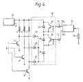
- FIG 4 shows a second embodiment of a drive circuit according to the present invention for driving the print head shown in Figure 1.
- each driving coil 5 for actuating respective levers 6 is connected at one end to a DC drive power circuit 60 and at the other end to ground through a respective switching transistor 61.
- the end of each driving coil 5 connected to the switching transistor 61 is also connected through a spark suppression circuit 62 to the DC drive power circuit 60.
- the spark suppression circuit 62 is composed of a plurality of series connected voltage regulation diodes 64, 65, 66 and forward connected with respect to the DC drive power circuit 60.
- One end of the series connected diodes 64, 65, 66 is connected to the DC drive power circuit 60, the other end is connected to connections between the driving coils 5 and the switching transistors 61 through respective diodes 63 reverse connected with respect to the DC drive power circuit 60.
- Two switching transistors 67, 68 of the spark suppression circuit 62 are connected across the diodes 64, 65, respectively.
- a spark potential suppression setting circuit 70 receives a signal from the temperature sensor 8 and delivers no H-level signal from first and second output terminals 70a, 70b thereof when the sensed temperature is within a set temperature range, delivers an H-level signal from the first output terminal 70a when the temperature of the print head is lower than the lower limit of the set temperature range, and delivers H-level signals from both first and second output terminals 70a, 70b when the temperature of the print head is higher than the upper limit of the set temperature range.
- the first output terminal 70a and the second output terminal 70b are connected to the base electrode of the switching transistor 66 and the base electrode of the switching transistor 68 respectively.
- Reference numerals 72, 73 indicate inverters.
- Waveform D shows the print data signal
- waveform SP shows conduction potential of the spark suppression circuit
- waveform H shows the driving coil current
- the driving coil 5 is supplied with a DC current I from the DC drive power circuit 60 and energised thereby, so that the lever 6 is attracted to cause the print wire to strike the platen 16.
- the driving coil 5 releases its electro-magnetic energy to generate a counter electro-motive force.
- a flywheel current I b1 is generated in the driving coil 5, which assists the motion of the lever 6 towards the platen 16.
- the lever 6 begins to return towards the damper member under the action of the return spring 12.
- the damper member 13 absorbs the impulse of the lever 6 having returned to the initial position under the action of the return spring 12, thereby preventing the lever 6 and the print wire 7 from rebound.
- the spark potential suppression setting circuit 70 delivers an H-level signal from the first output terminal 70a to make the switching transistor 67 conductive thereby short circuiting the diode 64.
- the conduction potential V2 of the spark suppression circuit 62 is lowered by the Zener voltage of the voltage regulation diode 64.
- the driving coil 5 releases its electro-magnetic energy to generate the counter electro-motive force.
- a flywheel current I b2 is generated in the driving coil 5, which assists the motion of the lever 6.
- the damper member can absorb the impulse of the lever 6 which has been decelerated by the attractive force of the driving coil 5, so that the lever 6 and the print wire 7 come to rest in the initial position without rebound.
- the spark potential suppression setting circuit 70 delivers H-level signals from the first output terminal 70a and the second output terminal 70b to make the switching transistors 67, 68 conductive thereby short circuiting the diodes 64, 65.
- the conduction potential V3 of the spark suppression circuit 62 lowers by the sum of the Zener voltages of the voltage regulation diodes 64, 65, as compared with the case where the temperature of the print head is within the set temperature range.
- the driving coil 5 is supplied with DC current from the DC drive power circuit 60 and energised thereby, so that the lever 6 is attracted to cause the print wire 7 to strike the platen 16.
- the driving coil 5 releases its electro-magnetic energy to generate a counter electro-motive force.
- a flywheel current I b3 is generated in the driving coil 5, which assists the motion of the lever 6.
- the conduction potential V3 of the spark suppression circuit 62 is reduced by the sum of the Zener voltages of the two voltage regulation diodes 64, 65 as compared with the case where the temperature of the print head is within the set temperature range, the flywheel current I b3 is still flowing through the driving coil 5 even as the lever 6 returns to the initial position. Therefore, the driving coil 5 maintains its attractive force for a relatively long period to urge the lever 6 towards the platen, so that the return action of the lever 6 is braked over a relatively long period.
- the damper member absorbs the impulse of the lever 6 which has been decelerated by the attractive force of the driving coil 5 so that the lever 6 and the print wire 7 come to rest in the initial position without rebound.
- the conduction potential may be set to a lower level.
Landscapes
- Engineering & Computer Science (AREA)
- Mechanical Engineering (AREA)
- Dot-Matrix Printers And Others (AREA)
- Impact Printers (AREA)
Applications Claiming Priority (6)
| Application Number | Priority Date | Filing Date | Title |
|---|---|---|---|
| JP31602/89 | 1989-02-10 | ||
| JP3160289 | 1989-02-10 | ||
| JP3311189 | 1989-02-13 | ||
| JP33111/89 | 1989-02-13 | ||
| JP289720/89 | 1989-11-06 | ||
| JP1289720A JP2867489B2 (ja) | 1989-02-10 | 1989-11-06 | ワイヤドット型印字ヘッドの駆動回路 |
Publications (2)
| Publication Number | Publication Date |
|---|---|
| EP0382465A1 true EP0382465A1 (fr) | 1990-08-16 |
| EP0382465B1 EP0382465B1 (fr) | 1993-06-16 |
Family
ID=27287379
Family Applications (1)
| Application Number | Title | Priority Date | Filing Date |
|---|---|---|---|
| EP90301211A Expired - Lifetime EP0382465B1 (fr) | 1989-02-10 | 1990-02-06 | Circuit de commande d'une tête d'impression par points à fils |
Country Status (5)
| Country | Link |
|---|---|
| US (1) | US5054941A (fr) |
| EP (1) | EP0382465B1 (fr) |
| DE (1) | DE69001911T2 (fr) |
| HK (1) | HK71895A (fr) |
| SG (1) | SG28391G (fr) |
Cited By (1)
| Publication number | Priority date | Publication date | Assignee | Title |
|---|---|---|---|---|
| CN107253396A (zh) * | 2013-08-30 | 2017-10-17 | 精工爱普生株式会社 | 液体喷出装置、打印头单元、以及驱动基板 |
Families Citing this family (2)
| Publication number | Priority date | Publication date | Assignee | Title |
|---|---|---|---|---|
| DE69319003T2 (de) * | 1992-03-06 | 1998-12-17 | Seiko Epson Corp., Tokio/Tokyo | Überhitzungschutz für eine Treiberspule in einem Nadelpunktdrucker |
| US9393901B2 (en) * | 2014-07-21 | 2016-07-19 | Kostal Of America | Turn signal systems and methods |
Citations (3)
| Publication number | Priority date | Publication date | Assignee | Title |
|---|---|---|---|---|
| US4333398A (en) * | 1980-11-06 | 1982-06-08 | General Electric Company | Driving force control system for impact printer |
| EP0288864A2 (fr) * | 1987-04-30 | 1988-11-02 | BULL HN INFORMATION SYSTEMS ITALIA S.p.A. | Circuit de commande pour tête d'impression par matrice de points |
| JPS63317370A (ja) * | 1987-06-19 | 1988-12-26 | Matsushita Electric Ind Co Ltd | 印字部材駆動装置 |
Family Cites Families (8)
| Publication number | Priority date | Publication date | Assignee | Title |
|---|---|---|---|---|
| JPS58160169A (ja) * | 1982-03-18 | 1983-09-22 | Shinko Electric Co Ltd | サ−マルプリンタ |
| US4697939A (en) * | 1982-09-17 | 1987-10-06 | Canon Kabushiki Kaisha | Wire dot printer with improved wire dot head |
| JPS5970585A (ja) * | 1982-10-15 | 1984-04-21 | Hitachi Ltd | 印字ヘツド |
| US4552064A (en) * | 1982-10-27 | 1985-11-12 | Sanders Royden C Jun | Dot matrix printers and print heads therefor |
| US4661002A (en) * | 1983-08-19 | 1987-04-28 | Canon Kabushiki Kaisha | Dot matrix printer |
| US4625137A (en) * | 1983-12-09 | 1986-11-25 | Nippon Telegraph & Telephone Public Corp. | Piezoelectric actuator using bimorph element |
| JPS6158783A (ja) * | 1984-08-31 | 1986-03-26 | Toshiba Corp | 印字装置 |
| US4776712A (en) * | 1984-10-25 | 1988-10-11 | Tokyo Electric Co., Ltd. | Ink-dot printer |
-
1990
- 1990-02-06 SG SG1995906509A patent/SG28391G/en unknown
- 1990-02-06 EP EP90301211A patent/EP0382465B1/fr not_active Expired - Lifetime
- 1990-02-06 DE DE9090301211T patent/DE69001911T2/de not_active Expired - Fee Related
- 1990-02-09 US US07/477,380 patent/US5054941A/en not_active Expired - Lifetime
-
1995
- 1995-05-11 HK HK71895A patent/HK71895A/xx not_active IP Right Cessation
Patent Citations (3)
| Publication number | Priority date | Publication date | Assignee | Title |
|---|---|---|---|---|
| US4333398A (en) * | 1980-11-06 | 1982-06-08 | General Electric Company | Driving force control system for impact printer |
| EP0288864A2 (fr) * | 1987-04-30 | 1988-11-02 | BULL HN INFORMATION SYSTEMS ITALIA S.p.A. | Circuit de commande pour tête d'impression par matrice de points |
| JPS63317370A (ja) * | 1987-06-19 | 1988-12-26 | Matsushita Electric Ind Co Ltd | 印字部材駆動装置 |
Non-Patent Citations (1)
| Title |
|---|
| PATENT ABSTRACTS OF JAPAN, unexamined applications, M field, vol. 10, no. 270, September 13, 1986 THE PATENT OFFICE JAPANESE GOVERNMENT page 100 M 517 * |
Cited By (1)
| Publication number | Priority date | Publication date | Assignee | Title |
|---|---|---|---|---|
| CN107253396A (zh) * | 2013-08-30 | 2017-10-17 | 精工爱普生株式会社 | 液体喷出装置、打印头单元、以及驱动基板 |
Also Published As
| Publication number | Publication date |
|---|---|
| DE69001911D1 (de) | 1993-07-22 |
| SG28391G (en) | 1995-09-01 |
| HK71895A (en) | 1995-05-19 |
| EP0382465B1 (fr) | 1993-06-16 |
| US5054941A (en) | 1991-10-08 |
| DE69001911T2 (de) | 1993-09-23 |
Similar Documents
| Publication | Publication Date | Title |
|---|---|---|
| EP0382465B1 (fr) | Circuit de commande d'une tête d'impression par points à fils | |
| EP0380352B1 (fr) | Circuit d'activation d'une tête d'impression d'une imprimante à aiguilles | |
| US5312193A (en) | Control device for a matrix printer | |
| US4242004A (en) | Dot matrix printhead driver | |
| US4850724A (en) | Control circuit for dot matrix printing head | |
| EP0387641A1 (fr) | Dispositif de réglage automatique de l'espacement pour tête d'impression | |
| JP2867489B2 (ja) | ワイヤドット型印字ヘッドの駆動回路 | |
| US5032031A (en) | Drive circuit for a matrix printer | |
| EP0395763B1 (fr) | Imprimante a impact par points | |
| US5071268A (en) | Wire-dot print head driving apparatus having sensing coils | |
| US3466507A (en) | Drive circuit | |
| US4842429A (en) | Type face striking system in an office writing machine | |
| JP2505866B2 (ja) | ワイヤドット印字ヘッドの制御装置 | |
| EP0318449A2 (fr) | Méthode et disposition pour commander l'opération d'une imprimante matricielle | |
| JP3426280B2 (ja) | ワイヤドットヘッドの駆動装置 | |
| JP2505532B2 (ja) | ワイヤドットインパクトプリンタ装置 | |
| JPH047308B2 (fr) | ||
| JPH0455115B2 (fr) | ||
| JP3284471B2 (ja) | ワイヤインパクト式プリンタ | |
| JPS5945209B2 (ja) | マグネツト駆動回路 | |
| JPH0577457A (ja) | インパクトプリンタ | |
| JPS62292444A (ja) | ワイヤドツト記録装置 | |
| JPH01146757A (ja) | プリンタ | |
| JPS63153156A (ja) | ワイヤドツトヘツド | |
| JPS6259051A (ja) | 磁気駆動回路 |
Legal Events
| Date | Code | Title | Description |
|---|---|---|---|
| PUAI | Public reference made under article 153(3) epc to a published international application that has entered the european phase |
Free format text: ORIGINAL CODE: 0009012 |
|
| AK | Designated contracting states |
Kind code of ref document: A1 Designated state(s): DE FR GB |
|
| 17P | Request for examination filed |
Effective date: 19910131 |
|
| 17Q | First examination report despatched |
Effective date: 19921030 |
|
| GRAA | (expected) grant |
Free format text: ORIGINAL CODE: 0009210 |
|
| AK | Designated contracting states |
Kind code of ref document: B1 Designated state(s): DE FR GB |
|
| REF | Corresponds to: |
Ref document number: 69001911 Country of ref document: DE Date of ref document: 19930722 |
|
| ET | Fr: translation filed | ||
| PLBE | No opposition filed within time limit |
Free format text: ORIGINAL CODE: 0009261 |
|
| STAA | Information on the status of an ep patent application or granted ep patent |
Free format text: STATUS: NO OPPOSITION FILED WITHIN TIME LIMIT |
|
| 26N | No opposition filed | ||
| REG | Reference to a national code |
Ref country code: GB Ref legal event code: IF02 |
|
| PGFP | Annual fee paid to national office [announced via postgrant information from national office to epo] |
Ref country code: GB Payment date: 20070131 Year of fee payment: 18 |
|
| PGFP | Annual fee paid to national office [announced via postgrant information from national office to epo] |
Ref country code: DE Payment date: 20070201 Year of fee payment: 18 |
|
| PGFP | Annual fee paid to national office [announced via postgrant information from national office to epo] |
Ref country code: FR Payment date: 20070208 Year of fee payment: 18 |
|
| GBPC | Gb: european patent ceased through non-payment of renewal fee |
Effective date: 20080206 |
|
| REG | Reference to a national code |
Ref country code: FR Ref legal event code: ST Effective date: 20081031 |
|
| PG25 | Lapsed in a contracting state [announced via postgrant information from national office to epo] |
Ref country code: DE Free format text: LAPSE BECAUSE OF NON-PAYMENT OF DUE FEES Effective date: 20080902 |
|
| PG25 | Lapsed in a contracting state [announced via postgrant information from national office to epo] |
Ref country code: FR Free format text: LAPSE BECAUSE OF NON-PAYMENT OF DUE FEES Effective date: 20080229 |
|
| PG25 | Lapsed in a contracting state [announced via postgrant information from national office to epo] |
Ref country code: GB Free format text: LAPSE BECAUSE OF NON-PAYMENT OF DUE FEES Effective date: 20080206 |