EP0376291A2 - Integrierter Halbleiterschaltkreis - Google Patents
Integrierter Halbleiterschaltkreis Download PDFInfo
- Publication number
- EP0376291A2 EP0376291A2 EP89124039A EP89124039A EP0376291A2 EP 0376291 A2 EP0376291 A2 EP 0376291A2 EP 89124039 A EP89124039 A EP 89124039A EP 89124039 A EP89124039 A EP 89124039A EP 0376291 A2 EP0376291 A2 EP 0376291A2
- Authority
- EP
- European Patent Office
- Prior art keywords
- integrated circuit
- bus line
- semiconductor integrated
- circuit according
- data
- Prior art date
- Legal status (The legal status is an assumption and is not a legal conclusion. Google has not performed a legal analysis and makes no representation as to the accuracy of the status listed.)
- Granted
Links
Images


Classifications
-
- H10W20/427—
-
- H—ELECTRICITY
- H10—SEMICONDUCTOR DEVICES; ELECTRIC SOLID-STATE DEVICES NOT OTHERWISE PROVIDED FOR
- H10D—INORGANIC ELECTRIC SEMICONDUCTOR DEVICES
- H10D84/00—Integrated devices formed in or on semiconductor substrates that comprise only semiconducting layers, e.g. on Si wafers or on GaAs-on-Si wafers
- H10D84/90—Masterslice integrated circuits
- H10D84/903—Masterslice integrated circuits comprising field effect technology
-
- H10W20/43—
Definitions
- the present invention relates to a semiconductor integrated circuit having an element region and a wiring region, wherein a data bus formed in the wiring region is driven by a bus driver circuit.
- Fig. 5 is a block diagram showing a layout of a common microcontroller.
- the microcontroller includes various function blocks such as CPU 11, ROM 12, RAM 13, timer 14 and I/O port 15. Data transfer among these function blocks is performed through data bus 16, which comprises signal lines for data transfer. Four signal lines are used in a 4-bit microcontroller and eight signal lines are used in an 8-bit microcontroller.
- Fig. 6 is a circuit diagram showing part of an 8-bit microcontroller having a layout such as shown in Fig. 5 and which includes data bus 16 having eight signal lines D0 to D7, timer 14, and I/O port 15.
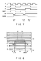
- Fig. 7 is a timing chart showing an example of data transfer performed using signal line D5 of data bus 16.
- control signal B is “0" when clock signal ⁇ is “1"
- control signal A is “1”
- data DATA1 is “1”
- data on signal line D5 is set at “0” by timer 14. Since no clock signal is supplied to latch circuit 26 in I/O port 15, output data DATA2 of latch circuit 26 does not vary. (period T2 in Fig. 7)
- the transfer of data depends on whether charges previously stored in the parasitic capacitance of the data bus during the precharge period are emitted or not.
- This method of data transfer has a drawback in that no data can be transferred during the precharge period when charges are stored in the parasitic capacitance of the data bus, but also has the advantage in that since the MOS transistors 23 and 24, which are used as bus drivers for driving the data bus, are both constituted by N-channel MOS transistors, the parasitic capacitance of the data bus is smaller than that of a CMOS type bus driver using both a P-channel and an N-channel MOS transistors, with the result that data can be transferred at high speed.
- Fig. 8 is a plan view showing a conventional pattern in which the N-channel MOS transistors 23 and 24 constituting a bus driver in the circuit shown in Fig. 6 are formed on an LSI.
- the components of Fig. 8 corresponding to those of Fig. 6 are indicated by the same reference numerals.
- Eight signal lines D0 to D7, constituting data bus 16, are made of metal such as aluminum and formed in wiring region 30 on a chip.
- Other signal lines 31 adjacent to signal line D7 are formed within wiring region 30.
- Signal lines 31 are also made of aluminum, as is power supply wire 33 for reference voltage (GND), and which is formed within element region 32 adjacent to signal line 31.
- GND reference voltage
- reference numerals 34, 35, and 36 denote N-type diffusion layers serving as the source and drain regions of N-channel MOS transistors 23 and 24.
- Diffusion layer 34 contacts signal line D5 through contact hole 37
- diffusion layer 36 contacts power supply wire 33 through contact hole 38.
- Polycrystalline silicon wire 39 which serves as a gate electrode of N-channel MOS transistor 23 and is supplied with signal A ⁇ ⁇ output from AND gate 22, is interposed between diffusion layers 34 and 35.
- polycrystalline silicon wire 40 which serves as a gate electrode of N-channel MOS transistor 24 and is supplied with data Data1 , is interposed between diffusion layers 35 and 36.
- the power supply wire for GND connected to the bus driver is formed within the element region and is used to constitute a logic circuit.
- various elements now shown, are formed between wiring region 30 and power supply wire 33 formed within element region 32.
- diffusion layer 36 is lengthened and an equivalent resistance in diffusion layer 36 is increased.
- the function blocks housed in the LSI perform complicated processings.
- Fig. 9 is a plan view showing a pattern corresponding to that of Fig. 8, wherein data is 32 bits in length and the number of signal lines of data bus 16 is increased up to 32 (D0 to D31), resulting in wiring region 30 being enlarged. With wiring region 30 enlarged, the length of diffusion layer 36 is greater than in the pattern shown in Fig. 8.
- Fig. 10 illustrates an equivalent circuit of the bus driver shown in Fig. 9. Since N type diffusion layer 36 is lengthened in this circuit, resistor R having a high resistance is equivalently inserted between the source of transistor 24 (shown in Fig. 8) and power supply wire 33 for GND in the bus driver. Consequently, the discharge characteristic of signal line D5 is degraded. More specifically, when signal line D5 is discharged, a current flows through two MOS transistors 23 and 24 and resistor R which are connected in series. Then, a voltage drop occurs on resistor R and the potential at the source region of transistor 24 is increased. As a result, transistor 24, which is operated at point a shown in Fig.
- the bus driver circuit is connected to the power supply wire formed in the element region through long diffusion layer 36 including resistive components, with the result that the discharge characteristic of the bus driver circuit is degraded and thus data cannot be transferred at high speed.
- An object of the present invention is to provide a semiconductor integrated circuit wherein data can be transferred in a data bus at high speed without degrading the discharge characteristic of a bus driver circuit.
- a semiconductor integrated circuit comprises a plurality of bus line means (D0 to D7) for transferring data, bus line driving means (34 to 39), connected to the bus line means (D0 to D7) and including one or more FETs, for determining a logical level of the bus line means (D0 to D7), and a ground potential wire (41) formed parallel to the bus line means (D0 to D7).
- a semiconductor integrated circuit having the above construction allows data to be transferred at high speed.
- the distance between the ground potential and the bus line driving means is comparatively long and these elements are connected to each other by extending a diffusion layer of an FET. For this reason, it takes time for charges to flow into the ground potential and for the potential of the bus line to become equal to the ground potential; accordingly, the processing speed of the semiconductor integrated circuit decreases.
- the ground potential wire is formed contiguous with the FET included in the bus line driving means, electrical resistance components are reduced and the time required for equalizing the potentials of the bus line and ground potential wire is shortened. In the semiconductor integrated circuit of the present invention, therefore, data processing can be performed at high speed.
- Fig. 1 is a plan view of a pattern of a semiconductor integrated circuit according to the first embodiment of the present invention.
- two N-channel MOS transistors, 23 and 24, constituting the bus driver shown in Fig. 6 are formed on an LSI.
- the components of Fig. 1 corresponding to those of Fig. 6 are represented by the same reference numerals.
- Data bus 16 comprises eight signal lines D0 to D7 which are made of metal such as aluminum and it is formed in wiring region 30 on a chip.
- GND reference voltage
- reference numerals 34, 35, and 36 denote N type diffusion layers which serve as a source and a drain regions of N-channel MOS transistors 23 and 24.
- Diffusion layer 34 is connected to a single signal line, e.g., signal line D5 through contact hole 37, and diffusion layer 36 is connected to power supply wire 41 through contact hole 38.
- Polycrystalline silicon wire 39 which serves as a gate electrode of N-channel MOS transistor 23 and is supplied with signal A ⁇ ⁇ from AND gate 22, is interposed between diffusion layers 34 and 35.
- polycrystalline silicon wire 40 which serves as a gate electrode of N-channel MOS transistor 24 and is supplied with data Datal, is interposed between diffusion layers 35 and 36.
- Fig. 2 is a cross-sectional view showing an element structure along the line of A - A′ of Fig. 1.
- numeral 42 indicates a P type substrate and 43 denotes a field oxide film.
- power supply wire 41 exclusively for the bus driver is formed within wiring region 30, and diffusion layer 36 of the N-channel MOS transistors functioning as the bus driver is connected to power supply wire 41. Since such elements formed within the element region as in the conventional circuit are not interposed between data bus 16 and power supply 41, diffusion layer 36 can therefore be shorter than the diffusion layer of the conventional circuit. As a result, the resistance of resistor R in the equivalent circuit shown in Fig. 10 can be lowered and degradation of the discharge characteristic of the data bus can thus be prevented. In other words, the data bus can be discharged in a short time and thus data can be transferred at high speed.
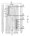
- Fig. 3 is a plan view showing a pattern of a semiconductor integrated circuit according to a second embodiment of the present invention.
- power supply wire 41 is arranged between signal lines D3 and D4 of the eight signal lines D0 to D7 constituting data bus 16.
- Fig. 3 shows bus driver 51 for driving signal line D7 of data bus 16 and bus driver 52 for driving signal line D1 of data bus 16.
- N type diffusion layers 53, 54, and 55 constitute the source and drain regions of two N-channel MOS transistors within bus driver 51.
- Diffusion layer 53 is connected to power supply wire 41 through contact hole 56 and diffusion layer 55 is connected to signal line D7 through contact hole 57.
- Polycrystalline silicon wire 58 which serves as a gate electrode of one of N-channel MOS transistors, is formed between diffusion layers 53 and 54, and polycrystalline silicon wire 59, which serves as a gate electrode of the other N-channel MOS transistor, is formed between diffusion layers 54 and 55.
- N type diffusion layers 60, 61, and 62 constitute the source and drain regions of two N-channel MOS transistors within bus driver 52. Diffusion layer 60 is connected to signal line D1 through contact hole 63 and diffusion layer 62 is connected to power supply wire 41 through contact hole 64.
- Polycrystalline silicon wire 65 which serves as a gate electrode of one of the N-channel MOS transistors, is formed between diffusion layers 60 and 61, and polycrystalline silicon wire 66, which serves as a gate electrode of the other N-channel MOS transistor, is formed between diffusion layers 61 and 62.
- signal line 67 is formed contiguous with signal line D0 of data bus 16
- signal line 68 is formed contiguous with signal line D7 thereof.
- the distance between power supply wire 41 and signal line D0 or D7 within data bus 16, which is the farthest from power supply wire 41 corresponds to the width of at most three signal lines.
- the distance between power supply wire 41 and signal line D0 within data bus 16, which is farthest from power supply wire 41 corresponds to the width of seven or more signal lines. Consequently, the longest discharge time of the data bus in the second embodiment can be made shorter than that of the data bus in the first embodiment.
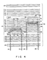
- Fig. 4 is a plan view showing a pattern of a semiconductor integrated circuit according to a third embodiment of the present invention.
- data bus 16 comprises 16 signal lines D0 to D15 and two power supply wires, 41A and 41B, which are arranged between the signal lines, power supply line 41A being arranged between signal lines D3 and D4, and power supply wire 41B arranged between signal lines D11 and D12.
- Fig. 4 illustrates bus driver 71 for driving signal line D9 of data bus 16 and bus driver 72 for driving signal line D7 of data bus 16.
- N type diffusion layers 73, 74, and 75 constitute the source and drain regions of two N-channel MOS transistors in bus driver 71.
- Diffusion layer 73 is connected to signal line D9 through contact hole 76, and diffusion layer 75 is connected to power supply wire 41B through contact hole 77.
- Polycrystalline silicon wire 78 which serves a gate electrode of one of the N-channel MOS transistors, is interposed between diffusion layers 73 and 74, and polycrystalline silicon wire 79, which serves as a gate electrode of the other N-channel MOS transistor, is interposed between diffusion layers 74 and 75.
- N type diffusion layers 80, 81, and 82 constitute the source and drain regions of two N-channel MOS transistors is bus driver 72.
- Diffusion layer 80 is connected to power supply wire 41A through contact hole 83, and diffusion layer 82 is connected to signal line D7 through contact hole 84.
- Polycrystalline silicon wire 85 which serves as a gate electrode of one of the N-channel MOS transistors, is interposed between diffusion layer 80 and 81, and polycrystalline silicon wire 86, which serves as a gate electrode of the other N-channel MOS transistor, is interposed between diffusion layers 81 and 82.
- signal line 67 is formed contiguous with signal line D0 of date bus 16 and signal line 68 is formed contiguous with signal line D7 thereof.
- the signal lines of the data bus are increased in number and wiring region 30 is enlarged, the number of power supply wires for GND formed within wiring region 30 is increased when the need arises.
- the signal lines of the data bus is increased in number and wiring region 30 is enlarged, the length of each diffusion layer connected to the power supply wire for GND can still be shorter than that in the case of the conventional apparatus.
- the number of the power supply wires is not limited to two but can be set to two or more in accordance with the number of signal lines constituting the data bus.
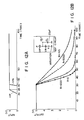
- Figs. 12A and 12B are a graph showing a simulation result obtained from the semiconductor integrated circuit according to the present invention.
- the resistance in the conventional circuit is 30 ⁇ and the resistance in the circuit of the present invention is 120 ⁇ or 1 K.
- Fig. 12B indicates that the circuit of a background art, to which the present invention is not applied, requires 10 nsec or 25 nsec from the turn on of 5 V to a time when the data bus potential (i.e., the potential of OUT) reaches to 2.5 V, while the circuit of the present invention requires only 6 nsec.
- the semiconductor integrated circuit according to the present invention is constructed such that the power supply wires exclusively for the bus driver circuit are arranged within the wiring region, data can be transferred at high speed without degrading the discharge characteristic of the bus driver circuit.
Landscapes
- Semiconductor Integrated Circuits (AREA)
- Design And Manufacture Of Integrated Circuits (AREA)
- Internal Circuitry In Semiconductor Integrated Circuit Devices (AREA)
Applications Claiming Priority (2)
| Application Number | Priority Date | Filing Date | Title |
|---|---|---|---|
| JP333615/88 | 1988-12-28 | ||
| JP63333615A JP2901188B2 (ja) | 1988-12-28 | 1988-12-28 | 半導体集積回路 |
Publications (3)
| Publication Number | Publication Date |
|---|---|
| EP0376291A2 true EP0376291A2 (de) | 1990-07-04 |
| EP0376291A3 EP0376291A3 (de) | 1991-01-30 |
| EP0376291B1 EP0376291B1 (de) | 1997-06-04 |
Family
ID=18268032
Family Applications (1)
| Application Number | Title | Priority Date | Filing Date |
|---|---|---|---|
| EP89124039A Expired - Lifetime EP0376291B1 (de) | 1988-12-28 | 1989-12-28 | Integrierter Halbleiterschaltkreis |
Country Status (4)
| Country | Link |
|---|---|
| EP (1) | EP0376291B1 (de) |
| JP (1) | JP2901188B2 (de) |
| KR (1) | KR930007183B1 (de) |
| DE (1) | DE68928096T2 (de) |
Cited By (1)
| Publication number | Priority date | Publication date | Assignee | Title |
|---|---|---|---|---|
| FR2682521A1 (fr) * | 1991-10-14 | 1993-04-16 | Samsung Electronics Co Ltd | Dispositif integre a memoire a semiconducteurs. |
Family Cites Families (4)
| Publication number | Priority date | Publication date | Assignee | Title |
|---|---|---|---|---|
| JPS6030170A (ja) * | 1983-07-29 | 1985-02-15 | Hitachi Ltd | 高集積読み出し専用メモリ |
| JPS6120349A (ja) * | 1984-07-06 | 1986-01-29 | Hitachi Ltd | Lsi集合体 |
| JPS63126263A (ja) * | 1986-11-17 | 1988-05-30 | Hitachi Ltd | 半導体集積回路装置 |
| JPS63229511A (ja) * | 1987-03-19 | 1988-09-26 | Matsushita Electric Ind Co Ltd | 半導体集積回路 |
-
1988
- 1988-12-28 JP JP63333615A patent/JP2901188B2/ja not_active Expired - Lifetime
-
1989
- 1989-12-21 KR KR1019890019153A patent/KR930007183B1/ko not_active Expired - Lifetime
- 1989-12-28 EP EP89124039A patent/EP0376291B1/de not_active Expired - Lifetime
- 1989-12-28 DE DE68928096T patent/DE68928096T2/de not_active Expired - Fee Related
Cited By (1)
| Publication number | Priority date | Publication date | Assignee | Title |
|---|---|---|---|---|
| FR2682521A1 (fr) * | 1991-10-14 | 1993-04-16 | Samsung Electronics Co Ltd | Dispositif integre a memoire a semiconducteurs. |
Also Published As
| Publication number | Publication date |
|---|---|
| KR900010782A (ko) | 1990-07-09 |
| DE68928096D1 (de) | 1997-07-10 |
| JPH03209757A (ja) | 1991-09-12 |
| JP2901188B2 (ja) | 1999-06-07 |
| EP0376291A3 (de) | 1991-01-30 |
| KR930007183B1 (ko) | 1993-07-31 |
| DE68928096T2 (de) | 1997-10-16 |
| EP0376291B1 (de) | 1997-06-04 |
Similar Documents
| Publication | Publication Date | Title |
|---|---|---|
| US8093657B2 (en) | Circuit and methods to improve the operation of SOI devices | |
| US4952825A (en) | Semiconductor integrated circuit having signal level conversion circuit | |
| JPH0897701A (ja) | 半導体回路 | |
| EP0350879B1 (de) | Ausgangstreiberschaltung für Halbleiter-IC | |
| US5301349A (en) | Single chip computer having ground wire formed immediately parallel a data bus and drivers formed directly under the data bus for high speed data transfer | |
| US5302871A (en) | Delay circuit | |
| US5023689A (en) | Complementary integrated circuit device equipped with latch-up preventing means | |
| JPH05343648A (ja) | マスタスライス方式半導体集積回路装置 | |
| US4859878A (en) | Bi-MOS levelshift circuit capable of controlling power consumption | |
| JPS61144056A (ja) | 半導体集積回路装置 | |
| EP0376291A2 (de) | Integrierter Halbleiterschaltkreis | |
| US4837461A (en) | Master slice type integrated circuit | |
| US5066996A (en) | Channelless gate array with a shared bipolar transistor | |
| US4631571A (en) | Semiconductor device for use in a large scale integration circuit | |
| JP3097200B2 (ja) | 半導体装置 | |
| JP3085472B2 (ja) | 半導体集積回路装置及びその形成方法 | |
| US6236234B1 (en) | High-speed low-power consumption interface circuit | |
| KR930011246B1 (ko) | 반도체장치 | |
| US6227637B1 (en) | Circuit and method for encoding and retrieving a bit of information | |
| JPH0680730B2 (ja) | 半導体集積回路チップ | |
| EP0032940B1 (de) | In serie gekoppelte transistoren verwendende igfet-dekodierschaltung | |
| KR100902476B1 (ko) | 디지털 rom 회로 및 디지털 판독 전용 데이터의 저장 방법 | |
| EP0302764B1 (de) | Schaltung zum Vergleichen binärer Signalamplituden | |
| JP3190191B2 (ja) | 出力バッファ回路 | |
| US5428255A (en) | Gate array base cell with multiple P-channel transistors |
Legal Events
| Date | Code | Title | Description |
|---|---|---|---|
| PUAI | Public reference made under article 153(3) epc to a published international application that has entered the european phase |
Free format text: ORIGINAL CODE: 0009012 |
|
| 17P | Request for examination filed |
Effective date: 19891228 |
|
| AK | Designated contracting states |
Kind code of ref document: A2 Designated state(s): DE FR GB |
|
| PUAL | Search report despatched |
Free format text: ORIGINAL CODE: 0009013 |
|
| RHK1 | Main classification (correction) |
Ipc: H01L 23/50 |
|
| AK | Designated contracting states |
Kind code of ref document: A3 Designated state(s): DE FR GB |
|
| 17Q | First examination report despatched |
Effective date: 19921102 |
|
| GRAG | Despatch of communication of intention to grant |
Free format text: ORIGINAL CODE: EPIDOS AGRA |
|
| GRAH | Despatch of communication of intention to grant a patent |
Free format text: ORIGINAL CODE: EPIDOS IGRA |
|
| GRAH | Despatch of communication of intention to grant a patent |
Free format text: ORIGINAL CODE: EPIDOS IGRA |
|
| GRAA | (expected) grant |
Free format text: ORIGINAL CODE: 0009210 |
|
| AK | Designated contracting states |
Kind code of ref document: B1 Designated state(s): DE FR GB |
|
| REF | Corresponds to: |
Ref document number: 68928096 Country of ref document: DE Date of ref document: 19970710 |
|
| ET | Fr: translation filed | ||
| PGFP | Annual fee paid to national office [announced via postgrant information from national office to epo] |
Ref country code: FR Payment date: 19971209 Year of fee payment: 9 |
|
| PGFP | Annual fee paid to national office [announced via postgrant information from national office to epo] |
Ref country code: GB Payment date: 19971219 Year of fee payment: 9 |
|
| PLBE | No opposition filed within time limit |
Free format text: ORIGINAL CODE: 0009261 |
|
| STAA | Information on the status of an ep patent application or granted ep patent |
Free format text: STATUS: NO OPPOSITION FILED WITHIN TIME LIMIT |
|
| 26N | No opposition filed | ||
| PG25 | Lapsed in a contracting state [announced via postgrant information from national office to epo] |
Ref country code: GB Free format text: LAPSE BECAUSE OF NON-PAYMENT OF DUE FEES Effective date: 19981228 |
|
| GBPC | Gb: european patent ceased through non-payment of renewal fee |
Effective date: 19981228 |
|
| PG25 | Lapsed in a contracting state [announced via postgrant information from national office to epo] |
Ref country code: FR Free format text: LAPSE BECAUSE OF NON-PAYMENT OF DUE FEES Effective date: 19990831 |
|
| REG | Reference to a national code |
Ref country code: FR Ref legal event code: ST |
|
| PGFP | Annual fee paid to national office [announced via postgrant information from national office to epo] |
Ref country code: DE Payment date: 20071220 Year of fee payment: 19 |
|
| PG25 | Lapsed in a contracting state [announced via postgrant information from national office to epo] |
Ref country code: DE Free format text: LAPSE BECAUSE OF NON-PAYMENT OF DUE FEES Effective date: 20090701 |