EP0367122B1 - Thermal head - Google Patents
Thermal head Download PDFInfo
- Publication number
- EP0367122B1 EP0367122B1 EP89119935A EP89119935A EP0367122B1 EP 0367122 B1 EP0367122 B1 EP 0367122B1 EP 89119935 A EP89119935 A EP 89119935A EP 89119935 A EP89119935 A EP 89119935A EP 0367122 B1 EP0367122 B1 EP 0367122B1
- Authority
- EP
- European Patent Office
- Prior art keywords
- thermal head
- layer
- heat
- metal
- protective layer
- Prior art date
- Legal status (The legal status is an assumption and is not a legal conclusion. Google has not performed a legal analysis and makes no representation as to the accuracy of the status listed.)
- Expired - Lifetime
Links
Images
Classifications
-
- B—PERFORMING OPERATIONS; TRANSPORTING
- B41—PRINTING; LINING MACHINES; TYPEWRITERS; STAMPS
- B41J—TYPEWRITERS; SELECTIVE PRINTING MECHANISMS, i.e. MECHANISMS PRINTING OTHERWISE THAN FROM A FORME; CORRECTION OF TYPOGRAPHICAL ERRORS
- B41J2/00—Typewriters or selective printing mechanisms characterised by the printing or marking process for which they are designed
- B41J2/315—Typewriters or selective printing mechanisms characterised by the printing or marking process for which they are designed characterised by selective application of heat to a heat sensitive printing or impression-transfer material
- B41J2/32—Typewriters or selective printing mechanisms characterised by the printing or marking process for which they are designed characterised by selective application of heat to a heat sensitive printing or impression-transfer material using thermal heads
- B41J2/335—Structure of thermal heads
- B41J2/33505—Constructional details
- B41J2/3353—Protective layers
-
- B—PERFORMING OPERATIONS; TRANSPORTING
- B41—PRINTING; LINING MACHINES; TYPEWRITERS; STAMPS
- B41J—TYPEWRITERS; SELECTIVE PRINTING MECHANISMS, i.e. MECHANISMS PRINTING OTHERWISE THAN FROM A FORME; CORRECTION OF TYPOGRAPHICAL ERRORS
- B41J2/00—Typewriters or selective printing mechanisms characterised by the printing or marking process for which they are designed
- B41J2/315—Typewriters or selective printing mechanisms characterised by the printing or marking process for which they are designed characterised by selective application of heat to a heat sensitive printing or impression-transfer material
- B41J2/32—Typewriters or selective printing mechanisms characterised by the printing or marking process for which they are designed characterised by selective application of heat to a heat sensitive printing or impression-transfer material using thermal heads
- B41J2/335—Structure of thermal heads
- B41J2/3355—Structure of thermal heads characterised by materials
-
- B—PERFORMING OPERATIONS; TRANSPORTING
- B41—PRINTING; LINING MACHINES; TYPEWRITERS; STAMPS
- B41J—TYPEWRITERS; SELECTIVE PRINTING MECHANISMS, i.e. MECHANISMS PRINTING OTHERWISE THAN FROM A FORME; CORRECTION OF TYPOGRAPHICAL ERRORS
- B41J2/00—Typewriters or selective printing mechanisms characterised by the printing or marking process for which they are designed
- B41J2/315—Typewriters or selective printing mechanisms characterised by the printing or marking process for which they are designed characterised by selective application of heat to a heat sensitive printing or impression-transfer material
- B41J2/32—Typewriters or selective printing mechanisms characterised by the printing or marking process for which they are designed characterised by selective application of heat to a heat sensitive printing or impression-transfer material using thermal heads
- B41J2/335—Structure of thermal heads
- B41J2/33555—Structure of thermal heads characterised by type
- B41J2/3357—Surface type resistors
Definitions
- the present invention relates to a thermal head and, more particularly, to an improvement in a protective layer of the thermal head.
- thermal head has been widely used in various recording devices such as a facsimile device and a word processor printer since the thermal head has advantages of noiseless, no need of maintenance, and a low running cost. Since such a recording device is required to be more compact, less expensive, and consume less power, a compact, inexpensive, and high-performance thermal head is also desired.
- Japanese Patent Disclosure (KOKAI) No. 52-100245 discloses a method in which a resin having a small thermal conductivity such as a polyimide resin or an epoxy resin is used as a heat insulating layer instead of conventional glazed glass. Since these resins have a low thermal diffusivity, the thermal heads using the resins have a high efficiency and can be easily bent to realize a compact size. A thermal head using such a polyimide resin as a heat insulating layer, however, cannot perform a stable printing operation for a long time period. The reasons for this are as follows. First, no polyimide resin having a sufficient heat resistance against an operation temperature of a thermal head can be obtained. Second, no sufficient adhesion between a resin and a substrate and between the resin and a thin film formed on the resin can be obtained not only under the static condition but also under the one of the repeated thermal stress.
- a resin having a small thermal conductivity such as a polyimide resin or an epoxy resin
- a siloxane-modified aromatic polyimide resin having a molecular structure represented by formula (1) as a material of a heat insulating layer so that a thermal head using a resin as a heat insulating layer can be put into practical use.
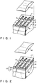
- a detailed structure of a thermal head of this type will be described below with reference to Fig. 1.
- reference numeral 1 denotes a metal substrate consisting of, e.g., an Fe-Cr alloy; and 2, a layer consisting of a polyimide resin represented by (formula 1).
- the polyimide resin layer 2 is obtained by coating and baking polyamic acid on the metal substrate 1.
- Polyamic acid is synthesized by substituting 0.05 to 10 mol% of p-phenylene diamine by bis-aminosiloxane upon ring-opening poly-addition reaction of an equimolar mixture of a biphenyl tetracarboxylic acid dihydride and p-phenylene diamine.
- Reference numeral 3 denotes an undercoating layer consisting of, e.g., SiO x , SiN, or SiC. The undercoating layer 3 is formed in order to protect the polyimide resin layer against chemical dry etching or ashing, facilitate control of a resistance upon formation of a heat-generating resistive layer 4, and improve a wire bonding property.
- Reference numeral 4 denotes a heat-generating resistor consisting of, e.g., Ta-SiO2 or Ti-SiO2.
- Discrete electrodes 6 and a common electrode 7 con sisting of, e.g., Al or Al-Si-Cu are formed on the heat-generating resistor 4 so as to form an opening to serve as a heat-generating portion 5.
- a protective layer 8 consisting of, e.g., Si-O-N, SiN, or SiC is formed so as to cover at least the heat-generating portion 5.
- the protective layer 8 is illustrated as a single layer in Fig. 1.
- a plurality of layers such as an oxidation-proofing layer and an abrasion-proofing layer may be formed independently from each other, or an oxidation-proofing/abrasion proofing layer and an adhesive layer may be formed.
- thermal head can sufficiently withstand an operation as a thermal head in terms of a heat-resistance and an adhesive force.
- a resistance abnormally changes to adversely affect a printing performance during the test.
- a singular point of a function at which the resistance abnormally changes as described above was carefully checked. As a result, it is found that hard foreign matters such as dust caught between the thermal head and heat-sensitive paper often causes a crack in the protective film, and the singular point of a function is produced when the crack reaches the heat-generating resistor.
- the surface protective layer Various materials, therefore, have been examined as the surface protective layer.
- Ta2O3 or SiO2 is unsatisfactory in hardness
- Si3N4, SiC, and Al2O3 is unsatisfactory in toughness
- materials of both these types produce cracks. That is, none of the material has sufficient properties to be used in the thermal head using a resin for the heat insulating layer.
- an example of a material not producing a crack is a SIALON film described in Japanese Patent Disclosure (KOKAI) Nos. 60-4077 and 62-3968. This SIALON film consists of Si, Al, O, and N as main components and has high hardness and toughness.
- a sputtering rate, however, upon formation of the SIALON film is low even in an Ar gas atmosphere.
- metal Al tends to precipitate to degrade an insulation property.
- this precipitation can be suppressed by adding 5% to 10% of O2 or N2 to the Ar gas, the sputtering rate is further decreased by this addition.
- a thermal head which comprises a high-resistance substrate, a heat-generating resistive layer formed on the high-resistance substrate, an electrode layer formed on the high-resistance substrate so as to be electrically connected to the heat-generating resistive layer, and a protective layer formed to cover at least a heat-generating portion of the heat-generating resistive layer.
- This protective layer consists of a compound containing Si, O, N, and a metal M which is at least one metal selected from the group consisting of Zr, Mg, and Y. Since the protective layer has high hardness and toughness, even if a local concentrated load acts on the protective layer during operation of the thermal head, the protective layer does not plastically deform much nor crack.
- this protective layer By using this protective layer, therefore, even if a heat insulating layer consisting of a soft material having high deformability such as a heat-resistant resin is included as an interlayer between the high-resistance substrate and the heat-generating resistive layer, since the protective layer has sufficient hardness for resisting deformation caused when a hard foreign matter is caught in and toughness which prevents a crack from being easily formed upon deformation to a certain extent, deformation, a crack, and the like caused by a local stress of the thermal head can be prevented. When this thermal head is used, reliability can be improved without degrading a printing performance. In addition, this protective layer can be formed at a higher sputtering rate than that of a conventional SIALON film and the like and is superior in a mass-production property.
- an Fe-Cr alloy for example, is used as a metal substrate 11.
- alloys containing, e.g., Al and Si in addition to Fe-Cr, and ceramics such as Al2O3 can also be used.
- a heat insulating layer 12 consisting of an aromatic polyimide resin represented by formula 1 below and having a thickness of about 5 to 50 »m, and preferably, 10 to 30 »m is formed as a heat insulating layer on the metal substrate 11. This polyimide resin is formed by coating and baking a polyamic acid varnish on the substrate 11.
- the polyamic acid varnish is prepared by substituting 5 mol% of p-phenylene diamine by bis-aminosiloxane to synthesize polyamic acid upon-ring opening poly-addition reaction of an equimolar mixture of, e.g., a biphenyl tetracarboxylic acid dihydride and p-phenylene diamine, and dissolving the obtained polyamic acid in an organic solvent.
- a polyamide resin, a polyamidoimide resin, a silicone resin, and the like can be used as the heat insulating layer 12.
- glazed glass can be used in place of the heat-resistant resin as a heat insulating layer 12, the substrate 11 and the heat insulating layer 12 are preferably a combination of a metal and a heat-resistant resin layer.
- the undercoating layer 13 is preferably constituted by at least one material selected from the group consisting of SiO x , SiON, SiN, SiC, and I-carbon.
- a heat-generating resistor 14 consisting of, e.g., Ta-SiO2 is formed on the undercoating layer 13, and discrete electrodes 16 and a common electrode 17 consisting of, e.g., Al are formed on the element 14.
- Heat-generating portions 15 are that parts of the heat-generating resistor 14 which are located between both the electrodes.
- a protective layer 18 consisting of a compound containing, e.g., Si, Zr, Y, N, and O is formed to cover the heat-generating portion 15, thereby completing the thermal head.
- the heat-generating resistor 14 of the heat-generating portion 15 when a pulse voltage is applied between the discrete and common electrodes 16 and 17 at a predetermined time interval, the heat-generating resistor 14 of the heat-generating portion 15 generates heat, thereby performing printing/recording.
- the present invention improves the protective film 18 of the thermal head.
- the film 18 consists of a compound containing Si, O, N, and a metal M (which is at least one metal selected from the group consisting of Zr, Mg, and Y).
- the film 18 preferably consists of a compound containing Si, O, N, Zr, and Y.
- an amount of Zr is preferably 1.0 to 40 mol% calculated in terms ot ZrO2. If the amount is less than 1.0 mol%, no sufficient hardness nor toughness can be obtained. If the amount exceeds 40 mol%, a large amount of a metal component is contained to degrade an insulation property of the protective layer.
- An amount of Y is preferably 0.1 to 10 mol% calculated in terms of Y2O3. If the amount is less than 0.1 mol%, no sufficient hardness nor toughness can be obtained. If the amount exceeds 10 mol%, a large amount of a metal component is contained to degrade the insulation property of the protective layer.
- An amount of Mg is preferably 0.1 to 10 mol% calculated in terms of MgO. If the amount is less than 0.1 mol%, no sufficient hardness nor toughness can be obtained. If the amount exceeds 10 mol%, a large amount of a metal component is contained to degrade the insulation property of the protective layer.
- the protective film 18 according to the present invention has higher hardness and toughness than those of a conventional protective film.
- a conventional SIALON film Al in the SIALON film properly disperses in the film as a metal component, thereby increasing the toughness.
- the hardness is increased since Zr and Y atoms bonded to N and O atoms are many as compared with Al atoms in SIALON, while a reduction in insulation property of the protective layer is small.
- a sputtering rate of the protective film according to the present invention is higher than that of the SIALON film and therefore is superior in a mass-production property.
- the thermal head of the present invention shown in Fig. 2 is manufactured, e.g., as follows.
- a metal substrate 11 consisting of an Fe alloy containing 18 wt% of Cr and having a thickness of about 0.5 mm is subjected to leveling, and cut into a predetermined size, and burr is removed therefrom. Thereafter, the metal substrate 11 is degreased/washed in an organic solvent, and dipped in diluted sulphuric acid maintained at 50°C to 70°C to remove an oxide layer formed on the surface and to perform an activation treatment to microscopically roughen the surface.
- the metal substrate 11 is washed with pure water and dried, and the above-described polyamic acid is adjusted to have a predetermined viscosity by using a solvent, e.g., N-methyl-2-pyrrolidone and coated on the metal substrate 11 to have a predetermined film thickness by using a roll coater, a spin coater, or the like.
- the resultant structure is heated in turn at 50°C for one hour, at 80°C for 30 minutes, at 120°C for 30 minutes, at 250°C for one hour, and at 450°C for one hour by using a sintering furnace to remove a solvent component and to accelerate a dehydrating cyclizing reaction so as to perform film formation, thereby forming a heat insulating layer 12.
- an undercoating layer 13 constituted by an SiN layer 31 and an SiC layer 32 is continuously formed on the heat insulating layer 12 at a substrate temperature of 150°C to 300°C by the plasma CVD method. That is, SiH4 gas and N2 gas are introduced to form the SiN layer 31, and then SiH4 gas and CH4 gas are introduced to form the SiC layer 32. Thereafter, a heat-generating resistor 14 consisting of Ta-SiO2, and discrete electrodes 16 and a common on electrode 17 consisting of Al are formed. Note that an opening serving to form a heat-generating portion 15 is obtained by forming an Al layer into a predetermined pattern by wet or dry etching after masking.
- Targets having compositions as listed in Table 1 below were used to perform sputtering in an Ar gas atmosphere in which a background pressure was 1 x 10 ⁇ 6 Torr and a pressure after Ar was introduced was 1 x 10 ⁇ 3 Torr, at a substrate temperature of 150°C to 200°C for a predetermined time, thereby forming protective films each having a film thickness of 3 »m.
- Each protective film was subjected to hardness estimation using a micro knoop hardness tester for thin films and fracture strength measurement using a scratch tester having a sensor for sensing acoustic emission generated upon film breaking.
- thermal heads having each protective film were assembled in facsimiles and operated, thereby performing a 10-km running test at a platen pressure of 160 g/cm and an application energy of 0.23 mJ/dot with a pulse width of 2.2 ms.
- the results are summarized in Table 1.
- Each layer thickness was 3 »m except for SiO2 (2 »m) + Ta2O5 (3 »m) in comparative examples.
- the protective layer according to the present invention has high hardness and toughness, can prevent a crack which tends to be produced when a resin is used as a heat insulating layer, can be produced at a high sputtering rate, and is superior in a mass-production property.
- a metal substrate is used as a support.
- the present invention is not limited to the above embodiment.
- a ceramic substrate or the like can be used.
Description
- The present invention relates to a thermal head and, more particularly, to an improvement in a protective layer of the thermal head.
- In recent years, a thermal head has been widely used in various recording devices such as a facsimile device and a word processor printer since the thermal head has advantages of noiseless, no need of maintenance, and a low running cost. Since such a recording device is required to be more compact, less expensive, and consume less power, a compact, inexpensive, and high-performance thermal head is also desired.
- In order to satisfy the above requirements, Japanese Patent Disclosure (KOKAI) No. 52-100245 discloses a method in which a resin having a small thermal conductivity such as a polyimide resin or an epoxy resin is used as a heat insulating layer instead of conventional glazed glass. Since these resins have a low thermal diffusivity, the thermal heads using the resins have a high efficiency and can be easily bent to realize a compact size. A thermal head using such a polyimide resin as a heat insulating layer, however, cannot perform a stable printing operation for a long time period. The reasons for this are as follows. First, no polyimide resin having a sufficient heat resistance against an operation temperature of a thermal head can be obtained. Second, no sufficient adhesion between a resin and a substrate and between the resin and a thin film formed on the resin can be obtained not only under the static condition but also under the one of the repeated thermal stress.
- The present inventors, however, have recently developed a siloxane-modified aromatic polyimide resin having a molecular structure represented by formula (1) as a material of a heat insulating layer so that a thermal head using a resin as a heat insulating layer can be put into practical use.

A detailed structure of a thermal head of this type will be described below with reference to Fig. 1. Referring to Fig. 1, reference numeral 1 denotes a metal substrate consisting of, e.g., an Fe-Cr alloy; and 2, a layer consisting of a polyimide resin represented by (formula 1). Thepolyimide resin layer 2 is obtained by coating and baking polyamic acid on the metal substrate 1. Polyamic acid is synthesized by substituting 0.05 to 10 mol% of p-phenylene diamine by bis-aminosiloxane upon ring-opening poly-addition reaction of an equimolar mixture of a biphenyl tetracarboxylic acid dihydride and p-phenylene diamine.Reference numeral 3 denotes an undercoating layer consisting of, e.g., SiOx, SiN, or SiC. The undercoatinglayer 3 is formed in order to protect the polyimide resin layer against chemical dry etching or ashing, facilitate control of a resistance upon formation of a heat-generatingresistive layer 4, and improve a wire bonding property.Reference numeral 4 denotes a heat-generating resistor consisting of, e.g., Ta-SiO₂ or Ti-SiO₂.Discrete electrodes 6 and acommon electrode 7 con sisting of, e.g., Aℓ or Aℓ-Si-Cu are formed on the heat-generatingresistor 4 so as to form an opening to serve as a heat-generating portion 5. Aprotective layer 8 consisting of, e.g., Si-O-N, SiN, or SiC is formed so as to cover at least the heat-generating portion 5. Theprotective layer 8 is illustrated as a single layer in Fig. 1. In an actual structure, however, a plurality of layers, such as an oxidation-proofing layer and an abrasion-proofing layer may be formed independently from each other, or an oxidation-proofing/abrasion proofing layer and an adhesive layer may be formed. - It is confirmed that such a thermal head can sufficiently withstand an operation as a thermal head in terms of a heat-resistance and an adhesive force. When this thermal head is incorporated in a device such as a facsimile device to perform a running test, however, a resistance abnormally changes to adversely affect a printing performance during the test. A singular point of a function at which the resistance abnormally changes as described above was carefully checked. As a result, it is found that hard foreign matters such as dust caught between the thermal head and heat-sensitive paper often causes a crack in the protective film, and the singular point of a function is produced when the crack reaches the heat-generating resistor. In addition, it is found that when a conventional high-resistance substrate obtained by forming glazed glass on Aℓ₂O₃ or a high-resistance substrate obtained by forming a glass layer on a metal substrate is used, the above phenomenon does not occur even if the other arrangements are the same. That is, it is found that this phenomenon particularly occurs when a resin is used as the heat insulating layer. It is assumed that the phenomenon occurs because a heat insulating layer consisting of glass having high hardness does not deform much upon operation of a thermal head while a heat insulating layer consisting of a resin largely deforms because a resin is soft. That is, when a concentrated load is locally applied on a thermal head, deformation of the surface protective layer is smaller than that of the resin layer. Therefore, the protective layer cannot follow the deformation of the resin layer and cracks.
- Various materials, therefore, have been examined as the surface protective layer. However, Ta₂O₃ or SiO₂, for example, is unsatisfactory in hardness, and Si₃N₄, SiC, and Aℓ₂O₃ is unsatisfactory in toughness, and materials of both these types produce cracks. That is, none of the material has sufficient properties to be used in the thermal head using a resin for the heat insulating layer. Of these various materials, an example of a material not producing a crack is a SIALON film described in Japanese Patent Disclosure (KOKAI) Nos. 60-4077 and 62-3968. This SIALON film consists of Si, Aℓ, O, and N as main components and has high hardness and toughness. A sputtering rate, however, upon formation of the SIALON film is low even in an Ar gas atmosphere. In addition, in this atmosphere, metal Aℓ tends to precipitate to degrade an insulation property. Although this precipitation can be suppressed by adding 5% to 10% of O₂ or N₂ to the Ar gas, the sputtering rate is further decreased by this addition.
- It is an object of the present invention to provide a thermal head having a protective layer which has high hardness, toughness and a superior mass-production property.
- According to the present invention, there is provided a thermal head which comprises a high-resistance substrate, a heat-generating resistive layer formed on the high-resistance substrate, an electrode layer formed on the high-resistance substrate so as to be electrically connected to the heat-generating resistive layer, and a protective layer formed to cover at least a heat-generating portion of the heat-generating resistive layer.
- This protective layer consists of a compound containing Si, O, N, and a metal M which is at least one metal selected from the group consisting of Zr, Mg, and Y. Since the protective layer has high hardness and toughness, even if a local concentrated load acts on the protective layer during operation of the thermal head, the protective layer does not plastically deform much nor crack. By using this protective layer, therefore, even if a heat insulating layer consisting of a soft material having high deformability such as a heat-resistant resin is included as an interlayer between the high-resistance substrate and the heat-generating resistive layer, since the protective layer has sufficient hardness for resisting deformation caused when a hard foreign matter is caught in and toughness which prevents a crack from being easily formed upon deformation to a certain extent, deformation, a crack, and the like caused by a local stress of the thermal head can be prevented. When this thermal head is used, reliability can be improved without degrading a printing performance. In addition, this protective layer can be formed at a higher sputtering rate than that of a conventional SIALON film and the like and is superior in a mass-production property.
- This invention can be more fully understood from the following detailed description when taken in conjunction with the accompanying drawings, in which:
- Fig. 1 is a perspective view showing a structure of a conventional thermal head; and
- Fig. 2 is a perspective view showing a thermal head according to an embodiment of the present invention.
- The present invention will be described in detail below with reference to the accompanying drawing.
- As shown in Fig. 2, in a thermal head of the present invention, an Fe-Cr alloy, for example, is used as a metal substrate 11. As the substrate, alloys containing, e.g., Aℓ and Si in addition to Fe-Cr, and ceramics such as Aℓ₂O₃ can also be used. A
heat insulating layer 12 consisting of an aromatic polyimide resin represented by formula 1 below and having a thickness of about 5 to 50 »m, and preferably, 10 to 30 »m is formed as a heat insulating layer on the metal substrate 11.
This polyimide resin is formed by coating and baking a polyamic acid varnish on the substrate 11. The polyamic acid varnish is prepared by substituting 5 mol% of p-phenylene diamine by bis-aminosiloxane to synthesize polyamic acid upon-ring opening poly-addition reaction of an equimolar mixture of, e.g., a biphenyl tetracarboxylic acid dihydride and p-phenylene diamine, and dissolving the obtained polyamic acid in an organic solvent. In addition to the polyimide resin, a polyamide resin, a polyamidoimide resin, a silicone resin, and the like can be used as theheat insulating layer 12. Although glazed glass can be used in place of the heat-resistant resin as aheat insulating layer 12, the substrate 11 and theheat insulating layer 12 are preferably a combination of a metal and a heat-resistant resin layer. - An undercoating
layer 13 constituted by two layers of anSiN layer 31 and anSiC layer 32 having a thickness of 1 to 5 »m, and preferably, 2 to 4 »m is formed on theheat insulating layer 12 by, e.g., a plasma CVD method. The undercoatinglayer 13 is preferably constituted by at least one material selected from the group consisting of SiOx, SiON, SiN, SiC, and I-carbon. - A heat-generating
resistor 14 consisting of, e.g., Ta-SiO₂ is formed on the undercoatinglayer 13, anddiscrete electrodes 16 and acommon electrode 17 consisting of, e.g., Aℓ are formed on theelement 14. Heat-generatingportions 15 are that parts of the heat-generatingresistor 14 which are located between both the electrodes. Aprotective layer 18 consisting of a compound containing, e.g., Si, Zr, Y, N, and O is formed to cover the heat-generatingportion 15, thereby completing the thermal head. - In this thermal head, when a pulse voltage is applied between the discrete and
common electrodes resistor 14 of the heat-generatingportion 15 generates heat, thereby performing printing/recording. - The present invention improves the
protective film 18 of the thermal head. Thefilm 18 consists of a compound containing Si, O, N, and a metal M (which is at least one metal selected from the group consisting of Zr, Mg, and Y). In addition, thefilm 18 preferably consists of a compound containing Si, O, N, Zr, and Y. - In the compound, an amount of Zr is preferably 1.0 to 40 mol% calculated in terms ot ZrO₂. If the amount is less than 1.0 mol%, no sufficient hardness nor toughness can be obtained. If the amount exceeds 40 mol%, a large amount of a metal component is contained to degrade an insulation property of the protective layer. An amount of Y is preferably 0.1 to 10 mol% calculated in terms of Y₂O₃. If the amount is less than 0.1 mol%, no sufficient hardness nor toughness can be obtained. If the amount exceeds 10 mol%, a large amount of a metal component is contained to degrade the insulation property of the protective layer. An amount of Mg is preferably 0.1 to 10 mol% calculated in terms of MgO. If the amount is less than 0.1 mol%, no sufficient hardness nor toughness can be obtained. If the amount exceeds 10 mol%, a large amount of a metal component is contained to degrade the insulation property of the protective layer.
- The
protective film 18 according to the present invention has higher hardness and toughness than those of a conventional protective film. For example, in a conventional SIALON film, Aℓ in the SIALON film properly disperses in the film as a metal component, thereby increasing the toughness. In the protective film according to the present invention, however, the hardness is increased since Zr and Y atoms bonded to N and O atoms are many as compared with Aℓ atoms in SIALON, while a reduction in insulation property of the protective layer is small. In addition, when the protective film is to be formed in an Ar gas atmosphere by sputtering, a sputtering rate of the protective film according to the present invention is higher than that of the SIALON film and therefore is superior in a mass-production property. - The thermal head of the present invention shown in Fig. 2 is manufactured, e.g., as follows.
- A metal substrate 11 consisting of an Fe alloy containing 18 wt% of Cr and having a thickness of about 0.5 mm is subjected to leveling, and cut into a predetermined size, and burr is removed therefrom. Thereafter, the metal substrate 11 is degreased/washed in an organic solvent, and dipped in diluted sulphuric acid maintained at 50°C to 70°C to remove an oxide layer formed on the surface and to perform an activation treatment to microscopically roughen the surface. Thereafter, the metal substrate 11 is washed with pure water and dried, and the above-described polyamic acid is adjusted to have a predetermined viscosity by using a solvent, e.g., N-methyl-2-pyrrolidone and coated on the metal substrate 11 to have a predetermined film thickness by using a roll coater, a spin coater, or the like. The resultant structure is heated in turn at 50°C for one hour, at 80°C for 30 minutes, at 120°C for 30 minutes, at 250°C for one hour, and at 450°C for one hour by using a sintering furnace to remove a solvent component and to accelerate a dehydrating cyclizing reaction so as to perform film formation, thereby forming a
heat insulating layer 12. - Thereafter, an
undercoating layer 13 constituted by anSiN layer 31 and anSiC layer 32 is continuously formed on theheat insulating layer 12 at a substrate temperature of 150°C to 300°C by the plasma CVD method. That is, SiH₄ gas and N₂ gas are introduced to form theSiN layer 31, and then SiH₄ gas and CH₄ gas are introduced to form theSiC layer 32. Thereafter, a heat-generatingresistor 14 consisting of Ta-SiO₂, anddiscrete electrodes 16 and a common onelectrode 17 consisting of Aℓ are formed. Note that an opening serving to form a heat-generatingportion 15 is obtained by forming an Aℓ layer into a predetermined pattern by wet or dry etching after masking. - Targets having compositions as listed in Table 1 below were used to perform sputtering in an Ar gas atmosphere in which a background pressure was 1 x 10⁻⁶ Torr and a pressure after Ar was introduced was 1 x 10⁻³ Torr, at a substrate temperature of 150°C to 200°C for a predetermined time, thereby forming protective films each having a film thickness of 3 »m. Each protective film was subjected to hardness estimation using a micro knoop hardness tester for thin films and fracture strength measurement using a scratch tester having a sensor for sensing acoustic emission generated upon film breaking. In addition, the thermal heads having each protective film were assembled in facsimiles and operated, thereby performing a 10-km running test at a platen pressure of 160 g/cm and an application energy of 0.23 mJ/dot with a pulse width of 2.2 ms. The results are summarized in Table 1. Each layer thickness was 3 »m except for SiO₂ (2 »m) + Ta₂O₅ (3 »m) in comparative examples.


- As is apparent from Table 1, the protective layer according to the present invention has high hardness and toughness, can prevent a crack which tends to be produced when a resin is used as a heat insulating layer, can be produced at a high sputtering rate, and is superior in a mass-production property.
- In the above embodiment, a metal substrate is used as a support. The present invention, however, is not limited to the above embodiment. For example, a ceramic substrate or the like can be used. In addition, even when glazed glass is used as a heat insulating layer, good results can be obtained.
Claims (9)
- A thermal head which comprises a high-resistance substrate (11), a heat-generating resistive layer (14) formed on the high-resistance substrate (11) and having a heat-generating portion (15), electrode layers (16, 17) formed on the high-resistance substrate (11) so as to be electrically connected to the heat-generating resistive element layer (14), and a protective layer (18) for covering at least the heat-generating portion (15) of the heat-generating resistive layer (14),
said protective layer (18) comprising a compound containing Si, O, N, and a metal M, characterized in that the metal M is at least one metal selected from the group consisting of Zr, Mg, and Y . - A thermal head according to claim 1, characterized in that the the metal M is at least one metal selected from the group consisting of Y and Zr.
- A thermal head according to claim 1, characterized in that the protective layer (18) comprises a compound containing Si, O, N, and Zr, the Zr content in the compound being 1.0 to 40 mol% calculated in terms of ZrO₂.
- A thermal head according to claim 1, characterized in that the protective layer (18) comprises a compound containing Si, O, N, and Y, the Y content in the compound being 0.1 to 10 mol% calculated in terms of Y₂O₃.
- A thermal head according to claim 1, characterized in that the high-resistance substrate (11) comprises one member selected from the group consisting of a metal, an alloy, and a ceramic.
- A thermal head according to claim 1, characterized in that heat insulating layer (12) comprising a heat-resistant resin is formed between the high-resistance substrate and the heat-generating resistive element layer (14).
- A thermal head according to claim 6, characterized in that the high-resistance substrate (11) comprises a metal.
- A thermal head according to claim 6, characterized in that the high-resistance substrate (11) comprises an alloy.
- A thermal head according to claim 6, characterized in that the high-resistance substrate (11) comprises a ceramic.
Applications Claiming Priority (2)
| Application Number | Priority Date | Filing Date | Title |
|---|---|---|---|
| JP63272943A JPH0626914B2 (en) | 1988-10-31 | 1988-10-31 | Thermal head |
| JP272943/88 | 1988-10-31 |
Publications (2)
| Publication Number | Publication Date |
|---|---|
| EP0367122A1 EP0367122A1 (en) | 1990-05-09 |
| EP0367122B1 true EP0367122B1 (en) | 1994-07-13 |
Family
ID=17520931
Family Applications (1)
| Application Number | Title | Priority Date | Filing Date |
|---|---|---|---|
| EP89119935A Expired - Lifetime EP0367122B1 (en) | 1988-10-31 | 1989-10-26 | Thermal head |
Country Status (5)
| Country | Link |
|---|---|
| US (1) | US4985712A (en) |
| EP (1) | EP0367122B1 (en) |
| JP (1) | JPH0626914B2 (en) |
| KR (1) | KR920010608B1 (en) |
| DE (1) | DE68916748T2 (en) |
Families Citing this family (2)
| Publication number | Priority date | Publication date | Assignee | Title |
|---|---|---|---|---|
| WO1997028965A1 (en) | 1996-02-08 | 1997-08-14 | Kabushiki Kaisha Toshiba | Thermal printing head, process for producing thermal printing head, recorder, sinter, and target |
| EP1226951A3 (en) * | 2001-01-29 | 2003-03-12 | Alps Electric Co., Ltd. | Power-saving thermal head |
Family Cites Families (11)
| Publication number | Priority date | Publication date | Assignee | Title |
|---|---|---|---|---|
| JPS52100245A (en) * | 1976-02-19 | 1977-08-23 | Oki Electric Ind Co Ltd | Thermal head of high heat efficiency |
| JPS5582677A (en) * | 1978-12-18 | 1980-06-21 | Toshiba Corp | Thermal head |
| JPS609770A (en) * | 1983-06-29 | 1985-01-18 | Kyocera Corp | Thermal head |
| JPS6135973A (en) * | 1984-07-30 | 1986-02-20 | Hitachi Ltd | Thermal head |
| JPS623968A (en) * | 1985-06-29 | 1987-01-09 | Noritake Co Ltd | Abrasion-resistant thin film thermal head |
| GB2179007B (en) * | 1985-08-12 | 1990-09-12 | Mitsubishi Electric Corp | Thermal head for printer |
| JPS6290260A (en) * | 1985-10-16 | 1987-04-24 | Tdk Corp | Antiwear protective film for thermal head |
| JPS62252101A (en) * | 1986-04-25 | 1987-11-02 | ティーディーケイ株式会社 | Resistive heating unit |
| DE3769860D1 (en) * | 1986-06-25 | 1991-06-13 | Toshiba Kawasaki Kk | HEAT HEAD. |
| JPS6374963A (en) * | 1986-09-16 | 1988-04-05 | 株式会社豊田中央研究所 | Silicon nitride base sintered body for antiabrasive material |
| JPS62275067A (en) * | 1987-05-16 | 1987-11-30 | 日本碍子株式会社 | Manufacture of silicon nitride sintered body |
-
1988
- 1988-10-31 JP JP63272943A patent/JPH0626914B2/en not_active Expired - Lifetime
-
1989
- 1989-10-26 EP EP89119935A patent/EP0367122B1/en not_active Expired - Lifetime
- 1989-10-26 US US07/426,865 patent/US4985712A/en not_active Expired - Lifetime
- 1989-10-26 DE DE68916748T patent/DE68916748T2/en not_active Expired - Lifetime
- 1989-10-31 KR KR1019890015675A patent/KR920010608B1/en not_active IP Right Cessation
Also Published As
| Publication number | Publication date |
|---|---|
| EP0367122A1 (en) | 1990-05-09 |
| DE68916748D1 (en) | 1994-08-18 |
| KR920010608B1 (en) | 1992-12-12 |
| US4985712A (en) | 1991-01-15 |
| JPH0626914B2 (en) | 1994-04-13 |
| KR900006133A (en) | 1990-05-07 |
| JPH02120057A (en) | 1990-05-08 |
| DE68916748T2 (en) | 1994-12-22 |
Similar Documents
| Publication | Publication Date | Title |
|---|---|---|
| US5831512A (en) | Resistance thermometer | |
| KR930004777B1 (en) | Heat resistant insulating coating material and thermal head making use thereof | |
| EP0367122B1 (en) | Thermal head | |
| JP2549135B2 (en) | Thermal head | |
| JP2928525B2 (en) | Sputtering target for protective film formation | |
| JP2888584B2 (en) | Sputter target Wear-resistant coating and thermal head using it | |
| JPH01202465A (en) | Protective coating material and thermal head using it | |
| JP4925537B2 (en) | Thermal head | |
| JP2549136B2 (en) | Thermal head | |
| JP4925535B2 (en) | Thermal head | |
| JPH0659737B2 (en) | Thermal head | |
| KR920005317B1 (en) | Heat-resistant insulating substrate thermal head and thermographic apparatus | |
| JP3323870B2 (en) | Thermal printer head | |
| JPH06256939A (en) | Sputtering target and high hardness film formed by using the same | |
| JPH048554A (en) | Heat-resistant insulating substrate and thermal head | |
| JP2568191Y2 (en) | Thermal head | |
| JPH0278573A (en) | Heat-resistant insulating substrate and thermal head | |
| JP4925536B2 (en) | Thermal head | |
| JPH0278576A (en) | Heat-resistant insulating substrate and thermal head | |
| KR920002533B1 (en) | Thermal head | |
| JPH03293164A (en) | Thermal head | |
| JPH05345433A (en) | Thermal head | |
| JPH07108695A (en) | Abrasion-resistant coat, and thermal head using the coat | |
| JPH0278575A (en) | Heat-resistant insulating substrate and thermal head | |
| JPS6156111B2 (en) |
Legal Events
| Date | Code | Title | Description |
|---|---|---|---|
| PUAI | Public reference made under article 153(3) epc to a published international application that has entered the european phase |
Free format text: ORIGINAL CODE: 0009012 |
|
| 17P | Request for examination filed |
Effective date: 19891123 |
|
| AK | Designated contracting states |
Kind code of ref document: A1 Designated state(s): DE FR GB |
|
| 17Q | First examination report despatched |
Effective date: 19930517 |
|
| GRAA | (expected) grant |
Free format text: ORIGINAL CODE: 0009210 |
|
| AK | Designated contracting states |
Kind code of ref document: B1 Designated state(s): DE FR GB |
|
| REF | Corresponds to: |
Ref document number: 68916748 Country of ref document: DE Date of ref document: 19940818 |
|
| ET | Fr: translation filed | ||
| PLBE | No opposition filed within time limit |
Free format text: ORIGINAL CODE: 0009261 |
|
| STAA | Information on the status of an ep patent application or granted ep patent |
Free format text: STATUS: NO OPPOSITION FILED WITHIN TIME LIMIT |
|
| 26N | No opposition filed | ||
| REG | Reference to a national code |
Ref country code: GB Ref legal event code: 746 Effective date: 19980909 |
|
| REG | Reference to a national code |
Ref country code: FR Ref legal event code: D6 |
|
| REG | Reference to a national code |
Ref country code: GB Ref legal event code: IF02 |
|
| PGFP | Annual fee paid to national office [announced via postgrant information from national office to epo] |
Ref country code: DE Payment date: 20081027 Year of fee payment: 20 |
|
| PGFP | Annual fee paid to national office [announced via postgrant information from national office to epo] |
Ref country code: FR Payment date: 20081014 Year of fee payment: 20 |
|
| PGFP | Annual fee paid to national office [announced via postgrant information from national office to epo] |
Ref country code: GB Payment date: 20081022 Year of fee payment: 20 |
|
| REG | Reference to a national code |
Ref country code: GB Ref legal event code: PE20 Expiry date: 20091025 |
|
| PG25 | Lapsed in a contracting state [announced via postgrant information from national office to epo] |
Ref country code: GB Free format text: LAPSE BECAUSE OF EXPIRATION OF PROTECTION Effective date: 20091025 |