EP0366235A1 - Verfahren und Anordnung zur Überwachung - Google Patents
Verfahren und Anordnung zur Überwachung Download PDFInfo
- Publication number
- EP0366235A1 EP0366235A1 EP89308534A EP89308534A EP0366235A1 EP 0366235 A1 EP0366235 A1 EP 0366235A1 EP 89308534 A EP89308534 A EP 89308534A EP 89308534 A EP89308534 A EP 89308534A EP 0366235 A1 EP0366235 A1 EP 0366235A1
- Authority
- EP
- European Patent Office
- Prior art keywords
- image
- light
- array
- section
- values
- Prior art date
- Legal status (The legal status is an assumption and is not a legal conclusion. Google has not performed a legal analysis and makes no representation as to the accuracy of the status listed.)
- Granted
Links
- 238000012544 monitoring process Methods 0.000 title claims abstract description 27
- 238000000034 method Methods 0.000 title claims description 17
- 238000003860 storage Methods 0.000 claims abstract description 51
- 238000012546 transfer Methods 0.000 claims description 24
- 230000003287 optical effect Effects 0.000 claims description 6
- 230000001186 cumulative effect Effects 0.000 claims description 2
- 238000003908 quality control method Methods 0.000 abstract description 10
- 238000004458 analytical method Methods 0.000 abstract description 7
- 230000007547 defect Effects 0.000 abstract description 2
- 230000010354 integration Effects 0.000 description 7
- 230000003111 delayed effect Effects 0.000 description 6
- 239000002131 composite material Substances 0.000 description 4
- 238000012545 processing Methods 0.000 description 4
- 230000008859 change Effects 0.000 description 3
- 239000013078 crystal Substances 0.000 description 3
- 239000000123 paper Substances 0.000 description 3
- 230000008569 process Effects 0.000 description 3
- 238000005070 sampling Methods 0.000 description 3
- 229920002799 BoPET Polymers 0.000 description 2
- 239000005041 Mylar™ Substances 0.000 description 2
- 229920001131 Pulp (paper) Polymers 0.000 description 2
- 239000011120 plywood Substances 0.000 description 2
- 229920003223 poly(pyromellitimide-1,4-diphenyl ether) Polymers 0.000 description 2
- 230000001360 synchronised effect Effects 0.000 description 2
- 125000000391 vinyl group Chemical group [H]C([*])=C([H])[H] 0.000 description 2
- 229920002554 vinyl polymer Polymers 0.000 description 2
- -1 CELANAR Polymers 0.000 description 1
- 230000009471 action Effects 0.000 description 1
- 230000002457 bidirectional effect Effects 0.000 description 1
- 238000006243 chemical reaction Methods 0.000 description 1
- 239000000109 continuous material Substances 0.000 description 1
- 238000010924 continuous production Methods 0.000 description 1
- 230000001419 dependent effect Effects 0.000 description 1
- 239000004744 fabric Substances 0.000 description 1
- 230000003760 hair shine Effects 0.000 description 1
- 230000002452 interceptive effect Effects 0.000 description 1
- 238000004519 manufacturing process Methods 0.000 description 1
- 239000000463 material Substances 0.000 description 1
- 239000000203 mixture Substances 0.000 description 1
- 230000010363 phase shift Effects 0.000 description 1
- 239000004033 plastic Substances 0.000 description 1
- 229920003023 plastic Polymers 0.000 description 1
- 239000000047 product Substances 0.000 description 1
- 230000009467 reduction Effects 0.000 description 1
- 238000012552 review Methods 0.000 description 1
- 238000011896 sensitive detection Methods 0.000 description 1
- 239000007787 solid Substances 0.000 description 1
- 229920002994 synthetic fiber Polymers 0.000 description 1
- 230000001960 triggered effect Effects 0.000 description 1
Images


Classifications
-
- G—PHYSICS
- G01—MEASURING; TESTING
- G01N—INVESTIGATING OR ANALYSING MATERIALS BY DETERMINING THEIR CHEMICAL OR PHYSICAL PROPERTIES
- G01N21/00—Investigating or analysing materials by the use of optical means, i.e. using sub-millimetre waves, infrared, visible or ultraviolet light
- G01N21/84—Systems specially adapted for particular applications
- G01N21/88—Investigating the presence of flaws or contamination
-
- H—ELECTRICITY
- H04—ELECTRIC COMMUNICATION TECHNIQUE
- H04N—PICTORIAL COMMUNICATION, e.g. TELEVISION
- H04N25/00—Circuitry of solid-state image sensors [SSIS]; Control thereof
- H04N25/70—SSIS architectures; Circuits associated therewith
- H04N25/71—Charge-coupled device [CCD] sensors; Charge-transfer registers specially adapted for CCD sensors
- H04N25/711—Time delay and integration [TDI] registers; TDI shift registers
-
- G—PHYSICS
- G01—MEASURING; TESTING
- G01N—INVESTIGATING OR ANALYSING MATERIALS BY DETERMINING THEIR CHEMICAL OR PHYSICAL PROPERTIES
- G01N21/00—Investigating or analysing materials by the use of optical means, i.e. using sub-millimetre waves, infrared, visible or ultraviolet light
- G01N21/84—Systems specially adapted for particular applications
- G01N21/88—Investigating the presence of flaws or contamination
- G01N21/89—Investigating the presence of flaws or contamination in moving material, e.g. running paper or textiles
-
- H—ELECTRICITY
- H04—ELECTRIC COMMUNICATION TECHNIQUE
- H04N—PICTORIAL COMMUNICATION, e.g. TELEVISION
- H04N5/00—Details of television systems
- H04N5/222—Studio circuitry; Studio devices; Studio equipment
- H04N5/253—Picture signal generating by scanning motion picture films or slide opaques, e.g. for telecine
-
- H—ELECTRICITY
- H04—ELECTRIC COMMUNICATION TECHNIQUE
- H04N—PICTORIAL COMMUNICATION, e.g. TELEVISION
- H04N7/00—Television systems
- H04N7/18—Closed-circuit television [CCTV] systems, i.e. systems in which the video signal is not broadcast
- H04N7/188—Capturing isolated or intermittent images triggered by the occurrence of a predetermined event, e.g. an object reaching a predetermined position
-
- G—PHYSICS
- G01—MEASURING; TESTING
- G01N—INVESTIGATING OR ANALYSING MATERIALS BY DETERMINING THEIR CHEMICAL OR PHYSICAL PROPERTIES
- G01N21/00—Investigating or analysing materials by the use of optical means, i.e. using sub-millimetre waves, infrared, visible or ultraviolet light
- G01N21/84—Systems specially adapted for particular applications
- G01N2021/845—Objects on a conveyor
-
- G—PHYSICS
- G01—MEASURING; TESTING
- G01N—INVESTIGATING OR ANALYSING MATERIALS BY DETERMINING THEIR CHEMICAL OR PHYSICAL PROPERTIES
- G01N21/00—Investigating or analysing materials by the use of optical means, i.e. using sub-millimetre waves, infrared, visible or ultraviolet light
- G01N21/84—Systems specially adapted for particular applications
- G01N21/88—Investigating the presence of flaws or contamination
- G01N21/8851—Scan or image signal processing specially adapted therefor, e.g. for scan signal adjustment, for detecting different kinds of defects, for compensating for structures, markings, edges
- G01N2021/8887—Scan or image signal processing specially adapted therefor, e.g. for scan signal adjustment, for detecting different kinds of defects, for compensating for structures, markings, edges based on image processing techniques
-
- G—PHYSICS
- G01—MEASURING; TESTING
- G01N—INVESTIGATING OR ANALYSING MATERIALS BY DETERMINING THEIR CHEMICAL OR PHYSICAL PROPERTIES
- G01N2201/00—Features of devices classified in G01N21/00
- G01N2201/10—Scanning
- G01N2201/102—Video camera
Definitions
- This invention relates to monitoring systems and methods.
- a video output signal was generated which included a long, continuous series of video image fields.
- a transfer CCD camera light was focused on an image section of a CCD sensor for a selected interval of time. The interval was selected to produce good image contrast with the amount of light received, e.g. 1/60th of a second.
- the charge on each element of the image section was indicative of received light intensity.
- the charge was transferred during a vertical blanking interval, e.g. a few hundred microseconds, into corresponding elements of an optically insensitive CCD mass storage section.
- the charge was read out element by element from the optically insensitive elements to form a video signal representing one field of the resultant image.
- the charge representing the second field was transferred from the image section to the storage section.
- the second video signal image section started integrating light to form a third field. This sequence was repeated cyclically to form a video signal representing a series of single image fields.
- a CCD device is asynchronously triggered at a controlled instant in time to "grab" a moving object.
- the instant in time is synchronized with the moving object's entry to a preselected examination point.
- a high intensity strobe is flashed concurrently with asynchronously triggering a CCD device to "grab" the moving object. While such a method has certain unique advantages, it requires a significant amount of power capacity to flash the high intensity light necessary for its functioning.
- the minimum cycle time of the strobe limited the speed of the conveying system.
- a monitoring system comprising: a conveying means for transporting an object to be examined through an examination region; an optical system for focusing light from the examination region onto an image section comprising an array of light sensitive elements which are each sensitive to light received through the optical system to produce individual pixel values that are indicative of an amount of light received; a transfer means for serially shifting the pixel values across the light sensitive elements to create a video signal representing an image of the examination region; and a control means for controlling the transfer means, characterised in that the pixel values are shifted in synchronization with movement of the conveying means.
- a monitoring system comprising: a charge coupled device array including: an image section comprising an array of light sensitive elements for accumulating pixel values indicative of a cumulative amount of light received; a storage section having an array of pixel storage elements, the storage section being electrically connected with the image section such that the pixel values can be transferred from the image section to the storage section; and a serializing means for serializing the pixel values from the storage section into a video signal; a conveying means for conveying a continuous web; means for continuously focusing light on the image section; a clock means for generating clock signals for transferring pixel values from the image section to the storage section, from the storage section to the serializing means and from the serializing means to produce said video signal; a monitoring means for monitoring the video signal for at least one preselected characteristic; and a recording means for recording any locations along the web corresponding to the monitored characteristic, characterised by synchronizing means operatively connected to the clock means for synchronizing the transfer of the pixel values at least
- a method of monitoring comprising the steps of: (a) moving an object to be examined through an examination region; (b) illuminating the object with light from a light source, as the object moves through the examination region; (c) projecting an image of the moving object onto an image sensor, the image moving across the image sensor with movement of the object; (d) shifting integrated light values formed in the image sensor along the image sensor from the image sensor to an output register; (e) syncronizing the movement of the object through the examination region and the shifting of the integrated light values; (f) reading integrated light values from the output register in the form of a serial stream of pixels to produce a video signal representing a video image; and (g) monitoring at least one characteristic of the object from the video signal.
- the system comprises a conveying means A which moves a continuous web or other object(s) to be examined through an examination region at an adjustable speed.
- a CCD camera or opto-electrical transducer system B monitors the moving object by focusing an image of the moving object on an opto-electric transducer. As the object moves, the image moves correspondingly along the transducer.
- a sycnchronizing control means C synchronizes and coordinates movement of the object and conversion of the image into an electronic video signal by the camera. Specifically, the transducer samples the same element or pixel of an image several times.
- the synchronizing means causes the multiple samplings corresponding to the same pixel of the image but sampled at different regions of the transducer to be integrated.
- the synchronising means preferably adapts the sampling of the transducer to movement of the object. However, in some applications it is advantageous to vary the speed of the object to match the sampling of the transducer.
- a quality control analysis means D analyses the video signal for flows, defects, or other characteristics of the web and denotes their locations.
- the conveying means A includes a conventional conveyor 10 for moving object 12 through the examination region 14.
- the conveyor includes rollers for a continuous web of floor coverings, wall paper, or other finished sheet goods.
- the continuous web may include polymeric films such as MYLAR, CELANAR, KAPTON, vinyls, plywood, paper products, etc.
- the conveyor may include a belt for carrying the articles.
- the conveyor may have pockets, recesses, or clamps for fixing the position of each received object on the belt.
- the examination region 14 is continuously illuminated by light from a lighting means 16.
- the camera B includes an optical system, such as a lens 20 , which focuses light received from the examination region on a light sensitive area 22 , preferably a bidirectional array of CCD elements.
- the lens focuses light emanating from the examination region continuously onto the light sensitive area or image section of the optoelectrical transducer.
- the resolution of the resultant image is determined by the number of CCD elements in each dimension. The more elements, the finer the resolution.
- a typical video camera might have a 244 x 610 element array. For color, three times as many elements are provided. A third of the elements have a green filter, a third have a blue filter, and a third have a red filter, or any other three color filter combination as is conventional in the art.
- the data is periodically shifted from the image section 22 to a light shielded storage section 24 during a vertical flyback period which erases or resets each element of the CCD image section.
- the vertical flyback signals are defeated and the image section and storage section transfer lines are both connected to the synchronizing means C to cause lines of pixels to be stepped continuously at a line frequency rate to output registers 26 .
- the object being imaged and its image on the CCD array move in precise synchronization with the shifting of charge values along the CCD array. For example, if the lens 20 focuses a 1 millimeter x 1 millimeter area of the object on each element of the CCD array, then each time the object moves 1 millimeter, the pixel or integrated light values are shifted one line in the CCD array. In this manner, subsequent images on the CCD array superimpose directly on shifted previous images. By the time an image value or line of image values reaches the optically insensitive storage section 24 of the sensor, the optic information from the object has been integrated over the entire transfer period (1/60 seconds, for example).
- each pixel value represents the sum of light received at each of 244 CCD elements.
- the synchronization means C keeps monitored object movement and the image sensor transfer process in precise synchronization.
- the speed of the conveyor rollers, drive motors, or the like is converted by the synchronization means into clocking signals for the CCD array.
- signals from clocking electronics in the camera may readjust and control the speed of the drive motors of the conveyor.
- clocking electronics 30 receives a trigger signal t i from a conveyor speed sensor or tachometer 32 and produces clock pulses ⁇ 1A - ⁇ 4A and ⁇ 1B - ⁇ 4B to clock the CCD array at a corresponding rate. More specifically, the trigger signals control the frequency of an image section transfer clock or means 34 , which supplies the clock signals to a light image sensor section control means 22a and a storage section control means 24a .
- the light image sensor control means 22a causes the charge of each image element or row of elements of the image section 22 to be shifted. More specifically, the four phase image section transfer clock signal ⁇ 1A - ⁇ 4A shifts the charge line by line. After just about 244 pulses or shift commands in the illustrated 244 active line image section embodiment, a line of charge values has been shifted 244 lines from the first line of the image section into the storage section 24 .
- the clocking signals are selected such that the image transfer is synchronized with the movement of the conveyor.
- the controller C conveys identical transfer clock pulses ⁇ 1B - ⁇ 4B to the storage section control means 24a as sent to the image section control means 22a to cause the data from the storage section 24 to be shifted line by line into the shift registers means 26 .
- the storage section is the same size as the image section. If the camera is limited to the time delayed integration mode, the storage section may be much smaller or even eliminated.
- a red shift register 26r For a color video image rendition, a red shift register 26r , a blue shift register 26b , and a green shift register 26g are provided.
- a shift register clocking means 36 sends higher speed three phase shift register clock signals ⁇ 1C - ⁇ 3C to a shift register controller 26a .
- the shift registers serially step each charge or data value onto video signal output lines 40 before the next line is loaded into the shift registers from the storage section.
- a number of shift register clock pulses equal to the number of elements per line are generated to clock out red, green, and blue output signals.
- Feedback amplifiers 42 combine each of the three color output signals with a feedback signal which establishes a DC reference level to minimize the interfering effects of clock noise.
- a gain adjusting amplifier means 44 adjusts the gain of all three signal components correspondingly.
- a black and white/color mode selecting means 46 selects whether a black and white or color composite video signal is to be produced.
- a summing means 50 sums the three color components corresponding to each pixel and feeds the data to a first video signal processing channel 52 .
- the video channel includes an impedance adjusting amplifier 54 for providing a low impedance output signal.
- a band pass filter 56 removes any vestiges of clocking signal noise or the like.
- a user controlled gain amplifier 58 amplifies the signal from the band pass filter and passes it to a clamping means 60 which restores the DC video. At the end of each horizontal sweep line, the clamping means shorts to a DC reference level to restore a DC level that sets the black level of the resultant image.
- a synchronization information means 62 switches between lines to reference voltages to add blanking and horizontal synchronization information to the signal.
- a feedback circuit 64 feeds back a portion of the composite video signal to provide a phase sensitive detection of the clocking to establish the DC level that minimizes the clock noise.
- the switching means 46 connects two components of the output signal to analogous video processing channels 52 ′, 52 ⁇ .
- the synchronization means 62 only adds synchronization information to one, generally the green, video component.
- the feedback signal also is based on a single one of the components.
- the video processing circuitry is stable to better than one part in 256 to enable precision digitizing and digital signal processing of the resultant video signal.
- the quality control analysis means D receives the composite video signal and operates on it in a manner that is appropriate to the quality control function undertaken.
- the analysis means D may turn the composite signal into a man-readable video image.
- the analysis means may examine components of the video signal corresponding to selected regions to determine whether they meet preselected characteristics relative to each other, preselected standards, or the like.
- the image of the web may change in gray scale or color relative to the rest of the web image.
- the change may be the result of color changes in the web or surface deformates that alter the amount of reflected light.
- the pixel values of the video signal of the web are compared with a preselected gray scale characteristic or value to determine if the web is deformed or damaged beyond selected tolerances. If the web has a repeating pattern, the image or video signal is compared with corresponding standards which change cyclically with the pattern to determine whether the web has been accurately processed. If the web is monitored in color, each image or pixel value of the video signal is compared with one of a plurality of colorimetric standards in accordance with a location within the pattern. Alternately, color or other physical parameters may be used to sort various types or grades of products. Numerous other sorting, quality control, and acceptance algorithms may be implemented as are appropriate to the requirements of the objects being examined.
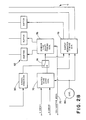
- the synchronizing means C further includes a 22.657 MHz internal crystal oscillator 70 for defining the image section transfer clock pulses in a normal interleaved frame video mode.
- the trigger signals t i from the tachometer 32 replace the crystal oscillator as the timing basis.
- the tachometer in the illustrated embodiment includes a light which shines through apertures of a disc attached to a guide roller that rotates with the conveying means and impinges on a photocell.
- the photocell sends a trigger pulse t i each time an incremental length of the scontinuous web product has passed through the examination region. In this manner, the trigger signal t i has a frequency that is proportional to the web speed.
- the frequency of the trigger signal is adjusted by the synchronization means to provide the timing of the transfer clock signals ⁇ 1A - ⁇ 4A , ⁇ 1B - ⁇ 4B , and ⁇ 1C - ⁇ 3C sent to the image section control means 22a , and storage section control means 24a , and the read out control means 26a .
- a high frequency detector 72 disables crystal oscillator 70 to synchronize the CCD camera with an external master clock signal, e.g. the trigger signal or other signal indicative of web movement.
- the trigger signal is frequency adjusted by dividers 74 , 76 to adjust a sync or master clock frequency generator 78 .
- Initialization pulses are received by a horizontal drive input 80 and vertical drive input 82 .
- the sync generator 78 synchronizes the horizontal and vertical drive pulses with the master clock signal.
- a multi norm pulse pattern generator (MNPPG) 84 is controlled by the sync generator and the vertical and horizontal drive signals to provide clock signals for the image section, storage section, and shift register of a conventional CCD video camera operation in a field or frame mode. Commonly, a first four phase clock signal is provided for the image section; a second four phase clock signal is provided for the storage section; and a three phase clock signal is provided for the shift registers.
- the multi-norm pulse pattern generator also provides transfer gate pulses TG1, optical blanking and clamping pulses, and start and stop pulses to reset the three phase clock.
- the pixel values in only the first line of the CCD array are refreshed each time. These pixel values are shifted along both the image and storage sections at a selectable speed and received light at each position is integrated. This is as opposed to the rapid transfer of pixel values from the image region to the storage region once per field in conventional operation.
- a processor 90 replaces the multi norm pulse pattern generator in the time delayed integration mode of the preferred embodiment.
- a frequency adjusting means 92 e.g. a frequency doubler, adjusts the master clock frequency as is appropriate to the number of lines of elements in the CCD array, the size of the examination region, and the magnification reduction of the camera optic system.
- a counter 94 counts the clock pulses whose frequency is determined by the tachometer 32 . With the illustrated 244 line CCD image section, a six bit counter is utilized such that each increment of the count (up to 244) causes the clock signal to shift the pixel values one line.
- a TDI wave generator 96 and a logic circuit 98 are addressed by the six bit signal to create and step the four phase clock signal in accordance with counted six bit value.
- the timing of the clock signal is such that the pixel values shift or step along the image and storage sections synchronously with the movement of the web. More specifically, the generator and logic circuit create a pair of four phase clock signals analogous to the MNPPG clock signals for shifting lines of data from the storage section into the shift register but without the pause for vertical blanking. In the preferred embodiment, the shifting is also at a slower speed than conventional.
- the three phase clock signal for the shift register is essentially the same as created by the MNPPG.
- the logic circuit 98 rests the counter 94 .
- a multiplexor 100 conveys the continuous four phase clock signals to vertical drivers 102 and 104 for the image and storage sections respectively. The outputs of the vertical drivers 102 , 104 are continuous four phase clock signals whose frequency and relative 1 phasing are determined by the tachometer 32 .
- the preferred embodiment can be operated either in the above described time delay integration mode or as a conventional video camera.
- an approximate input on the vertical driver input 82 causes a mode select means 106 to cause the multiplexor to send the above described TDI clock sequences to the vertical drivers 102 , 104 .
- An appropriate input on the horizontal drive input 80 initializes the six bit counter.
- conventional horizontal and vertical drive signals are applied at inputs 80 , 82 which enables the mode select means to cause the multiplexor to pass the conventional clocking output of the MNPPG 84 .
- the outside master clock signal is also reduced by a three phase clock divider 110 .
- a clock mix means 112 coordinates the three phase clock signals from the three phase clock divider 110 with the four phase image transfer clock signal.
- a voltage shift means 114 matches the three phase clock signal voltage with the video output shift register control 26a .
Landscapes
- Engineering & Computer Science (AREA)
- Multimedia (AREA)
- Signal Processing (AREA)
- Biochemistry (AREA)
- General Physics & Mathematics (AREA)
- Life Sciences & Earth Sciences (AREA)
- Chemical & Material Sciences (AREA)
- Analytical Chemistry (AREA)
- Physics & Mathematics (AREA)
- General Health & Medical Sciences (AREA)
- Health & Medical Sciences (AREA)
- Immunology (AREA)
- Pathology (AREA)
- Textile Engineering (AREA)
- Investigating Materials By The Use Of Optical Means Adapted For Particular Applications (AREA)
- Closed-Circuit Television Systems (AREA)
- Controlling Rewinding, Feeding, Winding, Or Abnormalities Of Webs (AREA)
- Image Input (AREA)
- Treatment Of Fiber Materials (AREA)
Applications Claiming Priority (2)
| Application Number | Priority Date | Filing Date | Title |
|---|---|---|---|
| US07249385 US4922337B1 (en) | 1988-04-26 | 1988-09-26 | Time delay and integration of images using a frame transfer ccd sensor |
| US249385 | 1994-05-25 |
Publications (3)
| Publication Number | Publication Date |
|---|---|
| EP0366235A1 true EP0366235A1 (de) | 1990-05-02 |
| EP0366235B1 EP0366235B1 (de) | 1995-06-07 |
| EP0366235B2 EP0366235B2 (de) | 2004-01-07 |
Family
ID=22943248
Family Applications (1)
| Application Number | Title | Priority Date | Filing Date |
|---|---|---|---|
| EP89308534A Expired - Lifetime EP0366235B2 (de) | 1988-09-26 | 1989-08-23 | Verfahren und Anordnung zur Überwachung |
Country Status (4)
| Country | Link |
|---|---|
| US (1) | US4922337B1 (de) |
| EP (1) | EP0366235B2 (de) |
| JP (1) | JP2955715B2 (de) |
| DE (1) | DE68922957T3 (de) |
Cited By (8)
| Publication number | Priority date | Publication date | Assignee | Title |
|---|---|---|---|---|
| FR2720259A1 (fr) * | 1994-05-31 | 1995-12-01 | Trophy Radiologie | Appareil de radiodiagnostic du type à capteur à transfert de charge. |
| EP1033881A3 (de) * | 1999-03-01 | 2002-06-05 | Honeywell Oy | Verfahren zur Synchronisation von Bilddaten eines mit Kameras überwachten Prozesses |
| WO2003039156A1 (en) * | 2001-11-02 | 2003-05-08 | Metso Paper Automation Oy | Flexible camera interface |
| WO2005004042A1 (en) * | 2003-07-08 | 2005-01-13 | Stora Enso Ab | Method and device for analysing surface structure in paper or board |
| FR2893810A1 (fr) * | 2005-11-23 | 2007-05-25 | Ercom Engineering Reseaux Comm | Procede de test de reseau de communication par l'intermediaire d'un terminal |
| EP1868366A1 (de) * | 2006-06-16 | 2007-12-19 | THOMSON Licensing | Verfahren zur Steuerung eines TDI-CCD Bildsensors |
| US7346411B2 (en) * | 2002-09-03 | 2008-03-18 | Continental Mabor-Industria De Pneus, S.A. | Automatic control and monitoring system for splice overlapping tolerance in textile ply |
| RU2532805C1 (ru) * | 2013-10-08 | 2014-11-10 | федеральное государственное бюджетное образовательное учреждение высшего профессионального образования "Ивановский государственный энергетический университет В.И. Ленина" (ИГЭУ) | Устройство для обнаружения металлических частиц в перемещаемом волокнистом материале |
Families Citing this family (63)
| Publication number | Priority date | Publication date | Assignee | Title |
|---|---|---|---|---|
| CA2078114A1 (en) * | 1990-03-13 | 1991-09-14 | Jean-Louis C. Guay | Web inspection system |
| JP2805659B2 (ja) * | 1990-09-06 | 1998-09-30 | ソニー株式会社 | ブレミッシュ補正装置 |
| US5113260A (en) * | 1990-12-24 | 1992-05-12 | Xerox Corporation | Sensor array for both synchronous and asynchronous operation |
| US5172005A (en) * | 1991-02-20 | 1992-12-15 | Pressco Technology, Inc. | Engineered lighting system for tdi inspection comprising means for controlling lighting elements in accordance with specimen displacement |
| US5365084A (en) * | 1991-02-20 | 1994-11-15 | Pressco Technology, Inc. | Video inspection system employing multiple spectrum LED illumination |
| US5149954A (en) * | 1991-03-26 | 1992-09-22 | Santa Barbara Research Center | Hold capacitor time delay and integration with equilibrating means |
| US5315366A (en) * | 1991-04-09 | 1994-05-24 | Murata Kikai Kabushiki Kaisha | Yarn package inspecting apparatus |
| US5148268A (en) * | 1991-04-26 | 1992-09-15 | Xerox Corporation | Multiplexing arrangement for controlling data produced by a color images sensor array |
| US5146340A (en) * | 1991-06-17 | 1992-09-08 | Georgia Tech Research Corporation | Image data reading and processing apparatus |
| DE4136461C2 (de) * | 1991-11-06 | 1999-04-08 | Roland Man Druckmasch | Vorrichtung und Verfahren zur großflächigen Bildinspektion |
| DE4137008A1 (de) * | 1991-11-11 | 1993-05-13 | Heribert F Dr Ing Broicher | Vorrichtung zur feststellung von qualitaetsaenderungen von massenguetern auf laufenden foerderbaendern |
| US5173748A (en) * | 1991-12-05 | 1992-12-22 | Eastman Kodak Company | Scanning multichannel spectrometry using a charge-coupled device (CCD) in time-delay integration (TDI) mode |
| DE69315465T2 (de) * | 1992-03-30 | 1998-05-28 | Ngk Insulators Ltd | Bildinformationspeicher und Bildinformationswiedergabegerät unter Verwendung eines Pockels-Modulators als optisches Ausleseelement |
| US5668887A (en) * | 1992-05-29 | 1997-09-16 | Eastman Kodak Company | Coating density analyzer and method using non-synchronous TDI camera |
| EP0572336B1 (de) * | 1992-05-29 | 2001-03-14 | Eastman Kodak Company | Vorrichtung und Verfahren zur Schichtdickenbestimmung mittels Bildverarbeitung |
| USH1740H (en) * | 1992-07-01 | 1998-07-07 | The United States Of America As Represented By The Secretary Of The Air Force | Synchronized rotating prism and CCD electrical readout color camera |
| US5301220A (en) * | 1992-09-03 | 1994-04-05 | Picker International, Inc. | Multi-mode acquisition x-ray imaging method and apparatus |
| DE4236302C1 (de) * | 1992-10-28 | 1993-12-16 | Erhardt & Leimer Gmbh | Verfahren und Anordnung zum Ausregeln seitlicher Abweichungen einer laufenden Warenbahn |
| US5650813A (en) * | 1992-11-20 | 1997-07-22 | Picker International, Inc. | Panoramic time delay and integration video camera system |
| US5747825A (en) * | 1992-11-20 | 1998-05-05 | Picker International, Inc. | Shadowgraphic x-ray imager with TDI camera and photo stimulable phosphor plate |
| AU6014594A (en) * | 1993-02-02 | 1994-08-29 | Golden Aluminum Company | Method and apparatus for imaging surfaces |
| US5847753A (en) * | 1993-04-16 | 1998-12-08 | Eastman Kodak Company | Camera system for scanning a moving surface |
| US5453781A (en) * | 1993-08-20 | 1995-09-26 | Hughes Aircraft Company | Apparatus and method for minimizing velocity-mismatch MTF degradation in TDI systems |
| US5434629A (en) * | 1993-12-20 | 1995-07-18 | Focus Automation Systems Inc. | Real-time line scan processor |
| DE4431669B4 (de) * | 1994-09-06 | 2006-01-12 | Heidelberger Druckmaschinen Ag | Vorrichtung zum Ablegen von mit einer Druckmaschine im fortlaufenden Betrieb erstellten, unterschiedlichen Produkten |
| GB2298542A (en) * | 1995-02-28 | 1996-09-04 | Pearpoint Ltd | Image motion compensation |
| US5767980A (en) * | 1995-06-20 | 1998-06-16 | Goss Graphic Systems, Inc. | Video based color sensing device for a printing press control system |
| US5696591A (en) * | 1996-01-05 | 1997-12-09 | Eastman Kodak Company | Apparatus and method for detecting longitudinally oriented flaws in a moving web |
| US5628574A (en) * | 1996-03-19 | 1997-05-13 | Roll Systems, Inc. | Web error recovery divert system |
| US5848189A (en) * | 1996-03-25 | 1998-12-08 | Focus Automation Systems Inc. | Method, apparatus and system for verification of patterns |
| US5682413A (en) * | 1996-06-21 | 1997-10-28 | Picker International, Inc. | Rotational angiography dye and mask image acquisition and synchronization |
| FR2754058B1 (fr) * | 1996-10-02 | 1998-12-18 | Etat Francais Laboratoire Cent | Procede de detection de defauts de surface sur une surface texturee |
| US5899959A (en) * | 1996-10-25 | 1999-05-04 | International Paper Company | Measurement of visual characteristics of paper |
| US5898790A (en) * | 1996-11-05 | 1999-04-27 | Maxwell Technologies, Inc. | Digital imaging and analysis system |
| US6906749B1 (en) * | 1998-09-16 | 2005-06-14 | Dalsa, Inc. | CMOS TDI image sensor |
| US6301373B1 (en) * | 1998-10-01 | 2001-10-09 | Mcgill University | Paper quality determination and control using scale of formation data |
| FI110343B (fi) | 1999-02-25 | 2002-12-31 | Honeywell Oy | Paperikoneen ratakatkojen monitorointijärjestelmä |
| GB9920501D0 (en) | 1999-09-01 | 1999-11-03 | Ncr Int Inc | Imaging system |
| EP1370830A1 (de) * | 2001-03-13 | 2003-12-17 | Tacshot, Inc. | Panoramaluftbildaufnahmevorrichtung |
| WO2003021242A1 (en) * | 2001-09-03 | 2003-03-13 | Millennium Venture Holdings Ltd. | Method and apparatus for inspecting the surface of workpieces |
| US6683293B1 (en) | 2002-04-26 | 2004-01-27 | Fairchild Imaging | TDI imager with target synchronization |
| US7102745B2 (en) * | 2003-06-17 | 2006-09-05 | Weatherford/Lamb, Inc. | Automated optical inspection of wire-wrapped well screens |
| WO2005075199A1 (en) * | 2004-02-06 | 2005-08-18 | Orlandi S.P.A. | A process and equipment for printing on non-woven-fabric |
| US7423280B2 (en) * | 2004-08-09 | 2008-09-09 | Quad/Tech, Inc. | Web inspection module including contact image sensors |
| EP1661702B1 (de) * | 2004-11-30 | 2007-05-09 | Oxy-Dry Maschinen GmbH | Verfahren und Vorrichtung zur Reinigung von Zylindern einer Druckmaschine |
| EP1761058B1 (de) * | 2005-08-31 | 2009-12-16 | Luc Van Quickelberge | Gerät und Verfahren zur Wiedergabe von Informationen aus unterschiedlichen Bildfrequenz dass die von Aufnahme |
| FI20065063A0 (fi) * | 2006-01-30 | 2006-01-30 | Visicamet Oy | Menetelmä ja mittalaite mitata pinnan siirtymä |
| US7855348B2 (en) * | 2006-07-07 | 2010-12-21 | Lockheed Martin Corporation | Multiple illumination sources to level spectral response for machine vision camera |
| US20080035866A1 (en) * | 2006-07-07 | 2008-02-14 | Lockheed Martin Corporation | Mail imaging system with UV illumination interrupt |
| US20080012981A1 (en) * | 2006-07-07 | 2008-01-17 | Goodwin Mark D | Mail processing system with dual camera assembly |
| US20080049972A1 (en) * | 2006-07-07 | 2008-02-28 | Lockheed Martin Corporation | Mail imaging system with secondary illumination/imaging window |
| US20080013069A1 (en) * | 2006-07-07 | 2008-01-17 | Lockheed Martin Corporation | Synchronization of strobed illumination with line scanning of camera |
| WO2008067509A1 (en) * | 2006-11-30 | 2008-06-05 | Westar Display Technologies, Inc. | Motion artifact measurement for display devices |
| JP2008213366A (ja) * | 2007-03-06 | 2008-09-18 | Ryobi Ltd | 印刷機におけるカラーバーの色濃度測定方法及び印刷機におけるカラーバーの色濃度測定装置並びに色濃度測定装置を備えた印刷機 |
| US20100147951A1 (en) * | 2008-12-11 | 2010-06-17 | Sik Piu Kwan | apparatus, method and system for reducing motion blur in an image capture device |
| JP5665107B2 (ja) | 2009-06-25 | 2015-02-04 | Nec東芝スペースシステム株式会社 | 撮像装置、撮像方法及び撮像回路 |
| US20110141269A1 (en) * | 2009-12-16 | 2011-06-16 | Stephen Michael Varga | Systems And Methods For Monitoring On-Line Webs Using Line Scan Cameras |
| CN104541500B (zh) * | 2012-10-12 | 2018-11-06 | 统雷有限公司 | 采用ccd成像仪的时间延迟与积分扫描 |
| US9176070B2 (en) * | 2014-04-07 | 2015-11-03 | Hseb Dresden Gmbh | Inspection assembly |
| US9357145B2 (en) | 2014-07-11 | 2016-05-31 | Imperx, Inc. | Area scan interline transfer CCD imaging device and apparatus with TDI scanning mode |
| CN109557104A (zh) * | 2018-11-19 | 2019-04-02 | 临沂众为智能科技有限公司 | 一种基于深度学习的木料优选锯智能检测方法 |
| CN113252564B (zh) * | 2021-05-25 | 2023-02-10 | 上海御微半导体技术有限公司 | 一种运动台与探测器同步控制的装置和方法 |
| KR102667266B1 (ko) * | 2021-12-03 | 2024-05-21 | 삼성전자주식회사 | 이미지 센서 및 이를 포함하는 스캐너 및 그 동작방법 |
Citations (7)
| Publication number | Priority date | Publication date | Assignee | Title |
|---|---|---|---|---|
| US3835332A (en) * | 1973-06-04 | 1974-09-10 | Eastman Kodak Co | Inspection apparatus for detecting defects in a web |
| US4223346A (en) * | 1979-04-05 | 1980-09-16 | Armco Inc. | Automatic defect detecting inspection apparatus |
| US4578810A (en) * | 1983-08-08 | 1986-03-25 | Itek Corporation | System for printed circuit board defect detection |
| EP0194331A1 (de) * | 1985-03-14 | 1986-09-17 | Toppan Printing Co., Ltd. | Einrichtung zum Überprüfen von Abdrücken |
| US4641256A (en) * | 1984-12-04 | 1987-02-03 | Rca Corporation | System and method for measuring energy transmission through a moving aperture pattern |
| EP0234492A2 (de) * | 1986-02-22 | 1987-09-02 | HELMUT K. PINSCH GMBH & CO. | Prüfvorrichtung und Verfahren für die Erfassung unterschiedlich ausgetalteter Oberflächen von Gegenständen |
| EP0311991A2 (de) * | 1987-10-14 | 1989-04-19 | Futec Incorporated | Verfahren und Vorrichtung zum Erkennen von kennzeichnenden Unterschieden in einem Blattmaterial |
Family Cites Families (12)
| Publication number | Priority date | Publication date | Assignee | Title |
|---|---|---|---|---|
| US32164A (en) * | 1861-04-23 | Stove | ||
| JPS5557103A (en) * | 1978-10-20 | 1980-04-26 | Nec Corp | Picture measuring device for mobile object |
| JPS55137391A (en) * | 1979-04-13 | 1980-10-27 | Hitachi Ltd | Spiral flow type blower |
| US4366574A (en) * | 1980-10-31 | 1982-12-28 | Technicare Corporation | Shadowgraphic slit scanner with video display |
| USRE32164E (en) | 1980-12-01 | 1986-05-27 | The University Of Utah | Radiographic systems employing multi-linear arrays of electronic radiation detectors |
| AU553069B2 (en) * | 1981-07-17 | 1986-07-03 | W.R. Grace & Co.-Conn. | Radial scan, pulsed light article inspection ccv system 0 |
| US4546444A (en) * | 1983-03-15 | 1985-10-08 | E. I. Du Pont De Nemours And Company | Data compression interface having parallel memory architecture |
| JPS6032488A (ja) * | 1983-08-02 | 1985-02-19 | Canon Inc | 撮像装置 |
| US4663669A (en) * | 1984-02-01 | 1987-05-05 | Canon Kabushiki Kaisha | Image sensing apparatus |
| US4668982A (en) * | 1985-06-17 | 1987-05-26 | The Perkin-Elmer Corporation | Misregistration/distortion correction scheme |
| US4811409A (en) * | 1985-09-12 | 1989-03-07 | Insystems, Inc. | Method and apparatus for detecting defect information in a holographic image pattern |
| JPS6352003A (ja) * | 1986-08-21 | 1988-03-05 | Omron Tateisi Electronics Co | 自動目視装置 |
-
1988
- 1988-09-26 US US07249385 patent/US4922337B1/en not_active Expired - Lifetime
-
1989
- 1989-08-23 EP EP89308534A patent/EP0366235B2/de not_active Expired - Lifetime
- 1989-08-23 DE DE68922957T patent/DE68922957T3/de not_active Expired - Fee Related
- 1989-09-22 JP JP1247905A patent/JP2955715B2/ja not_active Expired - Fee Related
Patent Citations (7)
| Publication number | Priority date | Publication date | Assignee | Title |
|---|---|---|---|---|
| US3835332A (en) * | 1973-06-04 | 1974-09-10 | Eastman Kodak Co | Inspection apparatus for detecting defects in a web |
| US4223346A (en) * | 1979-04-05 | 1980-09-16 | Armco Inc. | Automatic defect detecting inspection apparatus |
| US4578810A (en) * | 1983-08-08 | 1986-03-25 | Itek Corporation | System for printed circuit board defect detection |
| US4641256A (en) * | 1984-12-04 | 1987-02-03 | Rca Corporation | System and method for measuring energy transmission through a moving aperture pattern |
| EP0194331A1 (de) * | 1985-03-14 | 1986-09-17 | Toppan Printing Co., Ltd. | Einrichtung zum Überprüfen von Abdrücken |
| EP0234492A2 (de) * | 1986-02-22 | 1987-09-02 | HELMUT K. PINSCH GMBH & CO. | Prüfvorrichtung und Verfahren für die Erfassung unterschiedlich ausgetalteter Oberflächen von Gegenständen |
| EP0311991A2 (de) * | 1987-10-14 | 1989-04-19 | Futec Incorporated | Verfahren und Vorrichtung zum Erkennen von kennzeichnenden Unterschieden in einem Blattmaterial |
Cited By (16)
| Publication number | Priority date | Publication date | Assignee | Title |
|---|---|---|---|---|
| EP0685201A1 (de) * | 1994-05-31 | 1995-12-06 | Trophy Radiologie | Röntgendiagnostikeinrichtung mit Szintillator und CCD-Sensor |
| FR2720259A1 (fr) * | 1994-05-31 | 1995-12-01 | Trophy Radiologie | Appareil de radiodiagnostic du type à capteur à transfert de charge. |
| EP1033881A3 (de) * | 1999-03-01 | 2002-06-05 | Honeywell Oy | Verfahren zur Synchronisation von Bilddaten eines mit Kameras überwachten Prozesses |
| US6873353B1 (en) | 1999-03-01 | 2005-03-29 | Honeywell Oy | Method for synchronizing image data obtained from process monitoring cameras |
| WO2003039156A1 (en) * | 2001-11-02 | 2003-05-08 | Metso Paper Automation Oy | Flexible camera interface |
| US7346411B2 (en) * | 2002-09-03 | 2008-03-18 | Continental Mabor-Industria De Pneus, S.A. | Automatic control and monitoring system for splice overlapping tolerance in textile ply |
| US7510629B2 (en) | 2003-07-08 | 2009-03-31 | Stora Enso Ab | Method and device for analysing surface structure in paper or board |
| CN100394436C (zh) * | 2003-07-08 | 2008-06-11 | 斯托拉恩索公司 | 用于分析纸张或纸板中的表面结构的方法和装置 |
| WO2005004042A1 (en) * | 2003-07-08 | 2005-01-13 | Stora Enso Ab | Method and device for analysing surface structure in paper or board |
| WO2007060358A1 (fr) * | 2005-11-23 | 2007-05-31 | Ercom Engineering Reseaux Communications | Procédé de test de réseau de communication par l'intermédiaire d'un terminal |
| FR2893810A1 (fr) * | 2005-11-23 | 2007-05-25 | Ercom Engineering Reseaux Comm | Procede de test de reseau de communication par l'intermediaire d'un terminal |
| US7787384B2 (en) | 2005-11-23 | 2010-08-31 | Ercom Engineering Reseaux Communications | Method for testing a communication network by means of a terminal |
| EP1868366A1 (de) * | 2006-06-16 | 2007-12-19 | THOMSON Licensing | Verfahren zur Steuerung eines TDI-CCD Bildsensors |
| WO2007144304A1 (en) * | 2006-06-16 | 2007-12-21 | Thomson Licensing | Method for controlling a tdi-ccd image sensor |
| US8698890B2 (en) | 2006-06-16 | 2014-04-15 | Gvbb Holdings S.A.R.L. | Method for controlling a TDI-CCD image sensor |
| RU2532805C1 (ru) * | 2013-10-08 | 2014-11-10 | федеральное государственное бюджетное образовательное учреждение высшего профессионального образования "Ивановский государственный энергетический университет В.И. Ленина" (ИГЭУ) | Устройство для обнаружения металлических частиц в перемещаемом волокнистом материале |
Also Published As
| Publication number | Publication date |
|---|---|
| US4922337B1 (en) | 1994-05-03 |
| DE68922957T3 (de) | 2004-12-16 |
| EP0366235B1 (de) | 1995-06-07 |
| US4922337A (en) | 1990-05-01 |
| JPH02141647A (ja) | 1990-05-31 |
| DE68922957D1 (de) | 1995-07-13 |
| EP0366235B2 (de) | 2004-01-07 |
| JP2955715B2 (ja) | 1999-10-04 |
| DE68922957T2 (de) | 1995-10-19 |
Similar Documents
| Publication | Publication Date | Title |
|---|---|---|
| EP0366235B1 (de) | Verfahren und Anordnung zur Überwachung | |
| EP0369585B1 (de) | Videokamera für die Überwachung | |
| EP0471444B1 (de) | Videokamera | |
| US4896211A (en) | Asynchronously triggered single field transfer video camera | |
| EP0572479B1 (de) | Eingebaute beleuchtungsvorrichtung fur prufung mit laufzeitintegration | |
| US5428392A (en) | Strobing time-delayed and integration video camera system | |
| GB2261341A (en) | Method and apparatus for image inspection | |
| EP0383809A1 (de) | Zähler für gestapelte gegenstände. | |
| EP0093077B1 (de) | Beobachtungsvorrichtung | |
| USRE36047E (en) | Multi-mode TDI/raster-scan television camera system | |
| US6714283B2 (en) | Sensor and method for range measurements using a TDI device | |
| US6081613A (en) | System for inspecting an appearance of a printed circuit board | |
| US4920429A (en) | Exposure compensation for a line scan camera | |
| US5530562A (en) | Apparatus for image acquisition with speed compensation | |
| EP0273638B1 (de) | Bildabtastersysteme | |
| EP0496867B1 (de) | Vorrichtung zur lokalisation einer perforation | |
| US4949191A (en) | System for scanning an image on a moving surface | |
| JPH05107038A (ja) | 撮像装置 | |
| CA2051015C (en) | High resolution camera with hardware data compaction | |
| GB2042163A (en) | Streak image analyser | |
| JPH0422282A (ja) | 画像入力装置 |
Legal Events
| Date | Code | Title | Description |
|---|---|---|---|
| PUAI | Public reference made under article 153(3) epc to a published international application that has entered the european phase |
Free format text: ORIGINAL CODE: 0009012 |
|
| AK | Designated contracting states |
Kind code of ref document: A1 Designated state(s): DE FR GB NL |
|
| 17P | Request for examination filed |
Effective date: 19900912 |
|
| 17Q | First examination report despatched |
Effective date: 19920109 |
|
| GRAA | (expected) grant |
Free format text: ORIGINAL CODE: 0009210 |
|
| AK | Designated contracting states |
Kind code of ref document: B1 Designated state(s): DE FR GB NL |
|
| ET | Fr: translation filed | ||
| REF | Corresponds to: |
Ref document number: 68922957 Country of ref document: DE Date of ref document: 19950713 |
|
| PLBQ | Unpublished change to opponent data |
Free format text: ORIGINAL CODE: EPIDOS OPPO |
|
| PLBI | Opposition filed |
Free format text: ORIGINAL CODE: 0009260 |
|
| PLBF | Reply of patent proprietor to notice(s) of opposition |
Free format text: ORIGINAL CODE: EPIDOS OBSO |
|
| 26 | Opposition filed |
Opponent name: WESSEX TECHNOLOGY LIMITED Effective date: 19960306 |
|
| NLR1 | Nl: opposition has been filed with the epo |
Opponent name: WESSEX TECHNOLOGY LIMITED |
|
| PLBF | Reply of patent proprietor to notice(s) of opposition |
Free format text: ORIGINAL CODE: EPIDOS OBSO |
|
| PLBO | Opposition rejected |
Free format text: ORIGINAL CODE: EPIDOS REJO |
|
| APAC | Appeal dossier modified |
Free format text: ORIGINAL CODE: EPIDOS NOAPO |
|
| APAE | Appeal reference modified |
Free format text: ORIGINAL CODE: EPIDOS REFNO |
|
| APAC | Appeal dossier modified |
Free format text: ORIGINAL CODE: EPIDOS NOAPO |
|
| PLBQ | Unpublished change to opponent data |
Free format text: ORIGINAL CODE: EPIDOS OPPO |
|
| PLAB | Opposition data, opponent's data or that of the opponent's representative modified |
Free format text: ORIGINAL CODE: 0009299OPPO |
|
| R26 | Opposition filed (corrected) |
Opponent name: WESSEX TECHNOLOGY LIMITED Effective date: 19960306 |
|
| NLR1 | Nl: opposition has been filed with the epo |
Opponent name: WESSEX TECHNOLOGY LIMITED |
|
| PLBQ | Unpublished change to opponent data |
Free format text: ORIGINAL CODE: EPIDOS OPPO |
|
| PLAB | Opposition data, opponent's data or that of the opponent's representative modified |
Free format text: ORIGINAL CODE: 0009299OPPO |
|
| PLBI | Opposition filed |
Free format text: ORIGINAL CODE: 0009260 |
|
| 26 | Opposition filed |
Opponent name: WESSEX TECHNOLOGY OPTO-ELECTRONIC PRODUCTS LIMITED Effective date: 19960306 |
|
| APAC | Appeal dossier modified |
Free format text: ORIGINAL CODE: EPIDOS NOAPO |
|
| PLAW | Interlocutory decision in opposition |
Free format text: ORIGINAL CODE: EPIDOS IDOP |
|
| REG | Reference to a national code |
Ref country code: GB Ref legal event code: IF02 |
|
| PLAW | Interlocutory decision in opposition |
Free format text: ORIGINAL CODE: EPIDOS IDOP |
|
| PGFP | Annual fee paid to national office [announced via postgrant information from national office to epo] |
Ref country code: NL Payment date: 20020627 Year of fee payment: 14 |
|
| REG | Reference to a national code |
Ref country code: GB Ref legal event code: 746 Effective date: 20030811 |
|
| REG | Reference to a national code |
Ref country code: GB Ref legal event code: 732E |
|
| PUAH | Patent maintained in amended form |
Free format text: ORIGINAL CODE: 0009272 |
|
| STAA | Information on the status of an ep patent application or granted ep patent |
Free format text: STATUS: PATENT MAINTAINED AS AMENDED |
|
| 27A | Patent maintained in amended form |
Effective date: 20040107 |
|
| AK | Designated contracting states |
Kind code of ref document: B2 Designated state(s): DE FR GB NL |
|
| NLR2 | Nl: decision of opposition |
Effective date: 20040107 |
|
| PG25 | Lapsed in a contracting state [announced via postgrant information from national office to epo] |
Ref country code: NL Free format text: LAPSE BECAUSE OF NON-PAYMENT OF DUE FEES Effective date: 20040301 |
|
| REG | Reference to a national code |
Ref country code: FR Ref legal event code: CD |
|
| NLV4 | Nl: lapsed or anulled due to non-payment of the annual fee |
Effective date: 20040301 |
|
| REG | Reference to a national code |
Ref country code: FR Ref legal event code: TP |
|
| ET3 | Fr: translation filed ** decision concerning opposition | ||
| REG | Reference to a national code |
Ref country code: FR Ref legal event code: D6 |
|
| APAH | Appeal reference modified |
Free format text: ORIGINAL CODE: EPIDOSCREFNO |
|
| PGFP | Annual fee paid to national office [announced via postgrant information from national office to epo] |
Ref country code: GB Payment date: 20070925 Year of fee payment: 19 |
|
| PGFP | Annual fee paid to national office [announced via postgrant information from national office to epo] |
Ref country code: DE Payment date: 20071015 Year of fee payment: 19 |
|
| PGFP | Annual fee paid to national office [announced via postgrant information from national office to epo] |
Ref country code: FR Payment date: 20070807 Year of fee payment: 19 |
|
| GBPC | Gb: european patent ceased through non-payment of renewal fee |
Effective date: 20080823 |
|
| REG | Reference to a national code |
Ref country code: FR Ref legal event code: ST Effective date: 20090430 |
|
| PG25 | Lapsed in a contracting state [announced via postgrant information from national office to epo] |
Ref country code: FR Free format text: LAPSE BECAUSE OF NON-PAYMENT OF DUE FEES Effective date: 20080901 Ref country code: DE Free format text: LAPSE BECAUSE OF NON-PAYMENT OF DUE FEES Effective date: 20090303 |
|
| PG25 | Lapsed in a contracting state [announced via postgrant information from national office to epo] |
Ref country code: GB Free format text: LAPSE BECAUSE OF NON-PAYMENT OF DUE FEES Effective date: 20080823 |