EP0364931A2 - Filtre diélectrique avec un pôle d'amortissement accordable à une fréquence prédéterminée - Google Patents
Filtre diélectrique avec un pôle d'amortissement accordable à une fréquence prédéterminée Download PDFInfo
- Publication number
- EP0364931A2 EP0364931A2 EP89119190A EP89119190A EP0364931A2 EP 0364931 A2 EP0364931 A2 EP 0364931A2 EP 89119190 A EP89119190 A EP 89119190A EP 89119190 A EP89119190 A EP 89119190A EP 0364931 A2 EP0364931 A2 EP 0364931A2
- Authority
- EP
- European Patent Office
- Prior art keywords
- dielectric
- electrodes
- dielectric filter
- resonators
- adjustment
- Prior art date
- Legal status (The legal status is an assumption and is not a legal conclusion. Google has not performed a legal analysis and makes no representation as to the accuracy of the status listed.)
- Granted
Links
Images


Classifications
-
- H—ELECTRICITY
- H01—ELECTRIC ELEMENTS
- H01P—WAVEGUIDES; RESONATORS, LINES, OR OTHER DEVICES OF THE WAVEGUIDE TYPE
- H01P7/00—Resonators of the waveguide type
- H01P7/10—Dielectric resonators
-
- H—ELECTRICITY
- H01—ELECTRIC ELEMENTS
- H01P—WAVEGUIDES; RESONATORS, LINES, OR OTHER DEVICES OF THE WAVEGUIDE TYPE
- H01P1/00—Auxiliary devices
- H01P1/20—Frequency-selective devices, e.g. filters
- H01P1/201—Filters for transverse electromagnetic waves
- H01P1/205—Comb or interdigital filters; Cascaded coaxial cavities
- H01P1/2056—Comb filters or interdigital filters with metallised resonator holes in a dielectric block
-
- H—ELECTRICITY
- H01—ELECTRIC ELEMENTS
- H01P—WAVEGUIDES; RESONATORS, LINES, OR OTHER DEVICES OF THE WAVEGUIDE TYPE
- H01P1/00—Auxiliary devices
- H01P1/20—Frequency-selective devices, e.g. filters
- H01P1/201—Filters for transverse electromagnetic waves
- H01P1/205—Comb or interdigital filters; Cascaded coaxial cavities
Definitions
- the present invention generally relates to a dielectric filter applicable to an antenna duplexer of a car telephone and, more particularly, to a dielectric filter having an attenuation pole which is tunable to a predetermined frequency.
- a dielectric filter customarily has a plurality of dielectric resonators implemented by center electrodes which may be arranged substantially parallel to each other in a homogeneous monolithic block of dielectric material.
- the dielectric block is provided with an input electrode pattern and an output electrode pattern thereon.
- the dielectric resonators constitute a series resonance circuit in combination and define a pass band frequency of the filter.
- a conductive electrode pattern for frequency adjustment is provided on one surface of the dielectric block and connected to one end of each center conductor. Another conductive electrode pattern is provided on the above-mentioned surface of the dielectric block in such a manner as to intervene between nearby dielectric resonators for the purpose of adjusting coupling capacitance or coupling inductance.
- a metalized pattern is formed on opposite sides and bottom of the dielectric block and connected to ground.
- An insulated wire having an insulative coating is laid above the dielectric resonators and connected at one end to the metalized pattern and at the other end to the output electrode pattern.
- the insulated wire may be implemented as an ICXL-PVC wire having a diameter of 0.32 millimeter, for example.
- An ICXL-PVC wire is a wire having a single conductor and a coating of vinyl chloride, as well known in the art. Such an insulated wire has the following effect in the electrical aspect.
- the ICXL-PVC wire is connected to the output electrode pattern and spaced apart from the dielectric resonators of the dielectric filter by a predetermined distance. Since the dielectric resonators serve as ⁇ /4 semicoaxial resonators, the electric field is most intensive at their open end. A certain capacitance exists between the dielectric resonators and the ICXL-PVC wire which is spaced apart from the open end of the dielectric resonators, setting up capacitive coupling.
- a parallel resonance circuit is completed by the coupling capacitance between the ICXL-PVC wire and the dielectric resonators, self-inductances of the ICXL-PVC wire, coupling capacitance between the input electrode pattern and the dielectric resonator, coupling capacitance between the dielectric resonators themselves, and coupling capacitance between the dielectric resonators and the output electrode pattern.
- the resonance frequency of the parallel resonance circuit is the zero transmission point, i.e. , infinite attenuation point or attenuation pole.
- the parallel resonance circuit made up of the ⁇ /4 semicoaxial resonators defines a pass band.
- the prior art dielectric filter having the above construction has some problems left unsolved. Specifically, the use of an ICXL-PVC wire for achieving an attenuation pole makes it difficult to tune the attenuation pole to a predetermined frequency range. While the ICXL-PVC wire has to be surely fixed to the dielectric block in order to set up an accurate attenuation pole, the fixation is not easy and, therefore, the reliability of operation is not satisfactory. This, coupled with the poor tunability of the pole, adds to the cost involved in the fabrication of a high performance polar dielectric filter.
- a dielectric filter of the present invention has a homogenous monolithic block of dielectric material.
- a plurality of dielectric resonators have individual center conductors which are formed in the block of dielectric material substantially in parallel with each other.
- a plurality of conductive electrodes for adjustment are arranged on one side of the block of dielectric material, and each extends across one end of respective one of the center conductors. Either one of the distance between nearby ones of the dielectric resonators and the configuration of the electrodes for adjustment is changed to cause overcoupling on the basis of coupling inductance or coupling capacitance, whereby an attenuation pole of the dielectric filter is turned to an infinite frequency.
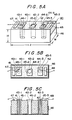
- the dielectric filter has a dielectric body 20 which is configured in a rectangular parallelepiped.
- the dielectric body 20 has a width W, a length l and a height H which may be 6. 0 millimeters, 20. 0 millimeters, and 8.8 millimeters, respectively.
- the dielectric body 20 is implemented as a homogeneous monolithic block of dielectric material.
- An input pin 21 and an output pin 22 each being made of a conductive material are disposed in the dielectric block 20 and extend to the upper end of the latter.
- a plurality of center conductors, three center conductors 23-1, 23-2 and 23-3 in the illustrative embodiment, are arranged substantially parallel to each other within the dielectric block 20, constituting dielectric resonators 24-1, 24-2 and 24-3.
- Conductive electrodes for frequency adjustments 25-1, 25-2 and 25-3 are provided on one side of the dielectric body 20, and each extends across respective one of the center conductors 23-1, 23-2 and 23-3.
- Electrodes 26-1 and 26-2 are interposed between the dielectric resonators 24-1 and 24-2 and between the dielectric resonators 24-2 and 24-3, respectively, each for adjusting coupling capacitance.
- a metalized layer 27 is formed on the front and rear ends, right and left sides and bottom of the dielectric body 20 and is connected to ground.
- a pair of electrodes 28 and 29 are positioned outwardly of the electrodes 25-1 and 25-3 with respect to the lengthwise direction of the dielectric body 20, serving to adjust the coupling capacitance.
- an electric signal applied to the input pin 21 causes the dielectric resonator 24-1 to generate an electromagnetic field.
- This electromagnetic field is transferred to the dielectric resonator 24-2 via the electrode 26-1 which is adapted for the adjustment of coupling capacitance.
- the dielectric field reached the dielectric resonator 24-2 is imparted to the dielectric resontor 24-3 via the electrode 26-2 with coupling capacitance being adjusted by the electrode 26-2. Consequently, an electric signal is fed to a load which is connected to the output pin 22.
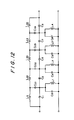
- FIG. 2 an equivalent circuit representative of lumped constants which are included in the dielectric filter of FIGS. 1A to 1C is shown.
- the equivalent LCs (inductance-capacitances) of the dielectric resonators 24-1, 24-2 and 24-3 are represented by ( l 1C1) ( l 2C2), and ( l 3C3), respectively.
- the coupling capacitance between the input pin 21 and the associated dielectric resonator 24-1 and the coupling capacitance between the output pin 22 and the associated dielectric resonator 24-3 are labeled C01 and C02, respectively.
- the coupling inductance developed by the adjusting electrode 26-1 and dielectric body 20 intervening between the successive dielectric resonators 24-1 and 24-2 is represented by l 12.
- the coupling capacitance developed by the adjusting electrode 26-2 and dielectric body 20 intervening between the successive dielectric resonators 24-2 and 24-3 is represented by l 23.
- the coupling capacitance between the dielectric resonators 24-1 and 24-3 located at the input and output stages, respectively, is labeled l p . Due to the coupling inductance l p , overcoupling occurs to produce a frequency f ⁇ which provides infinite attenuation, i.e., an attenuation pole in the high-frequency attenuation range of the pass band.
- the frequency f ⁇ exists due to the existence of the coupling inductance l p and occurs at the higher frequency side than the pass band.
- the frequency f ⁇ therefore, depends on the value of the coupling inductance l p .
- the coupling inductance l p can be set at any desired value and adjusted with ease by changing the pitch or distance of the dielectric resonators 24-1, 24-2 and 24-3 or the configuration of the electrodes 25-1, 25-2 and 25-3, as will be described.
- the dielectric filter shown in FIGS. 3A to 3C has a dielectric body 30 which is configured in a rectangular parallelepiped. Again, the dielectric body 30 has a width W, a lenght l and a height H which may be 6.0 millimeters, 20.0 millimeters, and 8.8 millimeters, respectively.
- the dielectric body 30 is implemented as a homogeneous monolithic block of dielectric material.
- An input pin 31 and an output pin 32 each being made of a conductive material are disposed in the dielectric block 20 and extend to the upper end of the latter.
- a plurality of center conductors, three center conductors 33-1, 33-2 and 33-3 in the illustrative embodiment, are arranged substantially parallel to each other within the dielectric block 20, constituting dielectric resonators 34-1, 34-2 and 34-3.
- Conductive electrodes for frequency adjustments 35-1, 35-2 and 35-3 are arranged on one side of the dielectric body 30, and each extends across one end of respective one of the center conductors 33-1, 33-2 and 33-3.
- a metalized layer 36 is formed on the front and rear ends, right and left sides and bottom of the dielectric body 30 and is connected to ground. Electrodes 37 and 38 are positioned outwardly of the electrodes 35-1 and 35-3 with respect to the lengthwise direction of the dielectric body 30, serving to adjust the coupling capacitance.
- the dielectric filter shown in Figs. 3A to 3C is void of the conductive patterns 26-1 and 26-2 which have been shown and described in the previous embodiment as being respectively interposed between the first- and second-stage dielectric resonators 24-1 and 24-2 and between the second- and third-stage dielectric resonators 24-2 and 24-3.
- FIG. 4 shows an equivalent circuit representative of lumped constants which are included in the dielectric filter of FIGS. 3A to 3C.
- the equivalent LCs of the dielectric resonators 34-1, 34-2 and 34-3 are represented by ( l 1C1), ( l 2C2) and ( l 3C3), respectively.
- the coupling capacitance between the input pin 31 and the associated dielectric resonator 34-1 and the coupling capacitance between the output pin 32 and the associated dielectric resonator 34-3 are labeled C01 and C02, respectively.
- the coupling capacitance between the nearby dielectric resonators 34-1 and 34-2 through the dielectric is represented by C12.
- the coupling capacitance between the dielectric resonators 34-2 and 34-3 through the dielectric is represented by C23.
- the coupling capacitance between the dielectric resonators 34-1 and 34-3 through the dielectric is labeled C p . Due to the coupling capacitance D p , overcoupling occurs to produce a frequency f ⁇ which provides infinite attenuation, i.e., an attenuation pole in the low-frequency attenuation range of the pass band.
- the coupling capacitance C p can be set at any desired value and adjusted with ease by changing the pitch or distance of the dielectric resonators 34-1, 34-2 and 34-3 or the configuration of the electrodes 35-1, 35-2 and 35-3.
- the dielectric filter also has a homogeneous monolithic block of dielectric, i.e., dielectric body 40 which is configured in a rectangular parallelepiped.
- the dielectric body 40 has a width W, a length l and a height H which may be 6.0 millimeters, 20.0 millimeters and 8.8 millimeters, respectively.
- the dielectric filter has an input pin 41, and output pin 42, a plurality of, three in the illustrative embodiment, center conductors 43-1, 43-2 and 43-3, dielectric resonators 44-1, 44-2 and 44-3, a plurality of patterns 45-1, 45-2 and 45-3 adapted for frequency adjustment, a metalized layer 46, and patterns 47 and 48 for the adjustment of coupling capacitance.
- These structural parts and elements are constructed and arranged in the same manner as in the dielectric filter of Figs. 1A to 1C.
- the dielectric filter shown in FIGS. 5A to 5C differs from the dielectric filter of FIGS. 1A to 1C in that it achieves the overcoupling coupling inductance l p or the overcoupling coupling capacitance C p by changing the configuration of the electrodes instead of the pitch of the dielectric resonators.
- FIGS. 6A to 6C depict a further alternative embodiment of the present invention.
- the dielectric filter has four elements disposed in a rectangular-parallelpiped monolithic block of dielectric 50.
- the dielectric filter accommodates an input pin 51, an output pin 52, a plurality of center conductors 54-1, 54-2, 54-3 and 54-4, a plurality of patterns for frequency adjustment 55-1, 55-2, 55-3 and 55-4, a metalized layer 56, and patterns for coupling capacitance adjustment 57, 58, 59, 60 and 61.
- the lumped constants of the dielectric filter of the illustrative embodiment may be represented by an equivalent circuit shown in FIG. 7.
- the equivalent LCs of the dielectric resonators 54-1, 54-2, 54-3 and 54-4 are labeled (L p 1 C p 1 ), (L p 2 C p 2 ), (L p 3 C p 3 ) and (L p 4 C p 4 ), respectively.
- the coupling capacitance between the input pin 51 and the first or input-stage dielectric resonator 54-1 is represented by C s 1
- the coupling capacitance between the output pin 52 and the fourth or output-stage dielectric resonator 54-4 by C s 5 is represented by C s 1
- the coupling capacitance between the third- and fourth-stage dielectric resonators 54-3 and 54-4 by C s 4 The coupling capacitance between the input pin 51 and the first or input-stage dielectric resonator 54-1 is represented by C s 1
- the coupling capacitance between the output pin 52 and the fourth or output-stage dielectric resonator 54-4 by C s 5 is represented by C s 1
- the coupling capacitance between the first- and third-stage dielectric resonators 54-1 and 54-3 or the coupling capacitance between second- and fourth-stage dielectric resonatos 54-2 and 54-4 is indicated by C ⁇ .
- Labeled R1 and R2 are a drive resistance and a terminal resistance, respectively.
- the four-element type dielectric filter shown in FIG. 6 was experimentally fabricated with a resonator pitch L of 5.0 millimeters, frequency f0 of 853 megahertz, frequency f - c of 840 megahertz, and frequency f + c of 866 megahertz.
- the frequency to attenuation characteristic measured with such a dielectric filter is represented by a curve a in FIG. 8.
- a curve b shown in FIG. 8 indicates a frequency to attenuation characteristic calculated with Q of 500. As shown, the actually measured characteristic is substantially coincident with the calculated characteristic.
- FIG. 9 shows the results of measurement obtained with dielectric filters which were different in pitch L from each other. As shown, the position where the frequency f ⁇ occurs is dependent on the pitch L.
- the dielectric filter has a dielectric block 10 which is provided with an input pattern 11, an output pattern 12, a plurality of center conductors 13-1, 13-2, 13-3 and 13-4, dielectric resonators 14-1, 14-2, 14-3 and 14-4, patterns 15-1, 15-2, 15-3 and 15-4 for frequency adjustment, and patterns 16-1, 16-2 and 16-3.
- a metalized pattern 17 is formed on the bottom and opposite sides of the dielectric block 10.
- FIG. 12 shows a lumped constant equivalent circuit associated with the dielectric filter of FIGS. 10 and 11.
- a parallel resonance circuit is constituted by coupling constants C c 1 , C c 2 , C c 3 and C c 4 between the wire 18 and the dielectric resonators 14-1 to 14-4, self-inductances L11, L22, L33, L44 and L55 of the wire 18, a coupling capacitance C1 between the input pattern 11 and the dielectric resonator 14-1, a coupling capacitance C3 between the dielectric resonators 14-1 and 14-2, a coupling capacitance C5 between the dielectric resonators 14-2 and 14-3, a coupling capacitance C7 between the dielectric resonators 14-3 and 14-4, and a coupling capacitance C9 between the dielectric resonator 14-4 and the output pattern 12.
- Such a circuit is successful in setting up an attenuation pole.
- any of the illustrative embodiments shown and described implements the attenuation pole by changing the distance between nearby dielectric resonators or the configuration of electrodes and not by using an insulated wire.
- a frequency which provides infinite attenuation in either one of a higher and a lower attenuation range of a pass band is achievable on the basis of the distance between nearby dielectric resonators or the configuration of electrodes. This eliminates the need for an extra external circuit otherwise affixed to a dielectric filter. Hence, the present invention can satisfy even strict standards with a minimum of filter stages, thereby implementing a miniature, high performance and inexpensive dielectric filter.
Landscapes
- Physics & Mathematics (AREA)
- Electromagnetism (AREA)
- Control Of Motors That Do Not Use Commutators (AREA)
Applications Claiming Priority (2)
| Application Number | Priority Date | Filing Date | Title |
|---|---|---|---|
| JP63260440A JPH07105644B2 (ja) | 1988-10-18 | 1988-10-18 | 有極型誘電体フィルタ |
| JP260440/88 | 1988-10-18 |
Publications (3)
| Publication Number | Publication Date |
|---|---|
| EP0364931A2 true EP0364931A2 (fr) | 1990-04-25 |
| EP0364931A3 EP0364931A3 (en) | 1990-11-22 |
| EP0364931B1 EP0364931B1 (fr) | 1994-08-24 |
Family
ID=17347966
Family Applications (1)
| Application Number | Title | Priority Date | Filing Date |
|---|---|---|---|
| EP89119190A Expired - Lifetime EP0364931B1 (fr) | 1988-10-18 | 1989-10-16 | Filtre diélectrique avec un pôle d'amortissement accordable à une fréquence prédéterminée |
Country Status (5)
| Country | Link |
|---|---|
| US (1) | US5150089A (fr) |
| EP (1) | EP0364931B1 (fr) |
| JP (1) | JPH07105644B2 (fr) |
| KR (1) | KR920009669B1 (fr) |
| DE (1) | DE68917676T2 (fr) |
Cited By (16)
| Publication number | Priority date | Publication date | Assignee | Title |
|---|---|---|---|---|
| EP0520665A2 (fr) * | 1991-06-25 | 1992-12-30 | Lk-Products Oy | Filtre diélectrique à température compensée |
| EP0520664A1 (fr) * | 1991-06-25 | 1992-12-30 | Lk-Products Oy | Filtre diélectrique |
| US5216394A (en) * | 1991-07-19 | 1993-06-01 | Uniden Corporation | Dielectric multi-line resonator including a coupling conductor line mainly inductively coupled to a resonator conductor line |
| US5227748A (en) * | 1990-08-16 | 1993-07-13 | Technophone Limited | Filter with electrically adjustable attenuation characteristic |
| USRE34898E (en) * | 1989-06-09 | 1995-04-11 | Lk-Products Oy | Ceramic band-pass filter |
| US5408206A (en) * | 1992-05-08 | 1995-04-18 | Lk-Products Oy | Resonator structure having a strip and groove serving as transmission line resonators |
| EP0738022A1 (fr) * | 1995-04-13 | 1996-10-16 | Thomson-Csf | Filtre passe-bande à cavités, à structure en peigne et radioaltimètre équipé d'un filtre d'entrée de ce type |
| EP0757401A2 (fr) * | 1995-08-04 | 1997-02-05 | Ngk Spark Plug Co., Ltd. | Filtre diélectrique |
| EP0825710A1 (fr) * | 1996-08-22 | 1998-02-25 | Matsushita Electric Industrial Co., Ltd. | Filtre avec amplificateur |
| CN1053998C (zh) * | 1995-05-31 | 2000-06-28 | 株式会社村田制作所 | 介质滤波器和天线转换开关 |
| US6313797B1 (en) * | 1998-10-22 | 2001-11-06 | Murata Manufacturing Co., Ltd. | Dielectric antenna including filter, dielectric antenna including duplexer, and radio apparatus |
| WO2007142786A1 (fr) * | 2006-05-31 | 2007-12-13 | Cts Corporation | filtre monobloc céramique avec couplage direct inductif et couplage croisé quadruple |
| US8269579B2 (en) | 2008-09-18 | 2012-09-18 | Cts Corporation | RF monoblock filter having an outwardly extending wall for mounting a lid filter thereon |
| US9030275B2 (en) | 2008-12-09 | 2015-05-12 | Cts Corporation | RF monoblock filter with recessed top pattern and cavity providing improved attenuation |
| US9030272B2 (en) | 2010-01-07 | 2015-05-12 | Cts Corporation | Duplex filter with recessed top pattern and cavity |
| US9030276B2 (en) | 2008-12-09 | 2015-05-12 | Cts Corporation | RF monoblock filter with a dielectric core and with a second filter disposed in a side surface of the dielectric core |
Families Citing this family (17)
| Publication number | Priority date | Publication date | Assignee | Title |
|---|---|---|---|---|
| US5227747A (en) * | 1989-06-15 | 1993-07-13 | Oki Electric Industry Co., Ltd. | Dielectric filter having coupling amount adjusting patterns |
| US5537085A (en) * | 1994-04-28 | 1996-07-16 | Motorola, Inc. | Interdigital ceramic filter with transmission zero |
| US5495215A (en) * | 1994-09-20 | 1996-02-27 | Motorola, Inc. | Coaxial resonator filter with variable reactance circuitry for adjusting bandwidth |
| US5666093A (en) * | 1995-08-11 | 1997-09-09 | D'ostilio; James Phillip | Mechanically tunable ceramic bandpass filter having moveable tabs |
| US5777276A (en) * | 1996-07-26 | 1998-07-07 | Micronics Computers Inc. | Mother board with auxiliary conductors in parallel with power connectors |
| JPH10135707A (ja) * | 1996-10-24 | 1998-05-22 | Ngk Spark Plug Co Ltd | 誘電体フィルタ |
| US6052040A (en) * | 1997-03-03 | 2000-04-18 | Ngk Spark Plug Co., Ltd. | Dielectric duplexer with different capacitive coupling between antenna pad and transmitting and receiving sections |
| US5850168A (en) * | 1997-04-18 | 1998-12-15 | Motorola Inc. | Ceramic transverse-electromagnetic-mode filter having a waveguide cavity mode frequency shifting void and method of tuning same |
| US5864265A (en) * | 1997-06-30 | 1999-01-26 | Motorola Inc. | Bandstop filter module with shunt zero |
| US5952900A (en) * | 1997-12-02 | 1999-09-14 | Cts Corporation | Suppression of spurious cavity modes using resistive paste on a ceramic transverse-electromagnetic-mode (TEM) filter |
| KR20020006098A (ko) * | 2000-07-11 | 2002-01-19 | 이형도 | 일체형 유전체 필터 |
| KR20020006097A (ko) * | 2000-07-11 | 2002-01-19 | 이형도 | 일체형 유전체 필터 |
| US6570473B2 (en) * | 2000-08-30 | 2003-05-27 | Tkd Corporation | Band pass filter |
| KR100446932B1 (ko) * | 2002-01-19 | 2004-09-04 | 센티스 주식회사 | 유전체필터 및 듀플렉서 유전체필터 |
| JP3864974B2 (ja) * | 2005-01-18 | 2007-01-10 | 株式会社村田製作所 | 誘電体フィルタ、誘電体デュプレクサおよび通信装置 |
| DE102014102521B4 (de) * | 2014-02-26 | 2023-10-19 | Snaptrack, Inc. | Abstimmbare HF-Filterschaltung |
| US10828426B2 (en) | 2018-04-06 | 2020-11-10 | Miller Medical Llc | Needle stick protection device |
Citations (5)
| Publication number | Priority date | Publication date | Assignee | Title |
|---|---|---|---|---|
| WO1983002853A1 (fr) * | 1982-02-16 | 1983-08-18 | Motorola Inc | Filtre ceramique passe-bande |
| JPS60254802A (ja) * | 1984-05-30 | 1985-12-16 | Murata Mfg Co Ltd | 分布定数形フイルタ |
| GB2163606A (en) * | 1984-08-21 | 1986-02-26 | Murata Manufacturing Co | Dielectric filter |
| GB2165098A (en) * | 1984-09-27 | 1986-04-03 | Motorola Inc | Radio frequency filters |
| US4716391A (en) * | 1986-07-25 | 1987-12-29 | Motorola, Inc. | Multiple resonator component-mountable filter |
Family Cites Families (13)
| Publication number | Priority date | Publication date | Assignee | Title |
|---|---|---|---|---|
| JPS57112101A (en) * | 1980-12-29 | 1982-07-13 | Fujitsu Ltd | Dielectric filter |
| US4768003A (en) * | 1984-09-28 | 1988-08-30 | Oki Electric Industry Co., Inc. | Microwave filter |
| JPS6180901A (ja) * | 1984-09-28 | 1986-04-24 | Oki Electric Ind Co Ltd | 誘電体共振器を用いたマイクロ波フイルタ |
| JPS6285002U (fr) * | 1985-11-18 | 1987-05-30 | ||
| JPS6354803A (ja) * | 1986-08-26 | 1988-03-09 | Oki Electric Ind Co Ltd | 誘電体フイルタ |
| JPS6354804A (ja) * | 1986-08-26 | 1988-03-09 | Oki Electric Ind Co Ltd | 誘電体フイルタ |
| JPS63124601A (ja) * | 1986-11-14 | 1988-05-28 | Oki Electric Ind Co Ltd | 誘電体フイルタ |
| JPH0612841B2 (ja) * | 1987-08-08 | 1994-02-16 | 沖電気工業株式会社 | 誘電体フィルタの周波数調整方法 |
| JPS6453603A (en) * | 1987-08-25 | 1989-03-01 | Oki Electric Ind Co Ltd | Polar type dielectric filter |
| JPH0713284Y2 (ja) * | 1987-09-21 | 1995-03-29 | 株式会社村田製作所 | 一体成形型誘電体フィルタの共振周波数調整構造 |
| JPH01112801A (ja) * | 1987-10-26 | 1989-05-01 | Kokusai Electric Co Ltd | 誘電体帯域フィルタ |
| JPH0652842B2 (ja) * | 1987-12-28 | 1994-07-06 | 沖電気工業株式会社 | 有極型誘電体フィルタ |
| US4965537A (en) * | 1988-06-06 | 1990-10-23 | Motorola Inc. | Tuneless monolithic ceramic filter manufactured by using an art-work mask process |
-
1988
- 1988-10-18 JP JP63260440A patent/JPH07105644B2/ja not_active Expired - Fee Related
-
1989
- 1989-10-16 DE DE68917676T patent/DE68917676T2/de not_active Expired - Fee Related
- 1989-10-16 EP EP89119190A patent/EP0364931B1/fr not_active Expired - Lifetime
- 1989-10-17 KR KR1019890014930A patent/KR920009669B1/ko not_active IP Right Cessation
-
1990
- 1990-12-26 US US07/641,252 patent/US5150089A/en not_active Expired - Lifetime
Patent Citations (5)
| Publication number | Priority date | Publication date | Assignee | Title |
|---|---|---|---|---|
| WO1983002853A1 (fr) * | 1982-02-16 | 1983-08-18 | Motorola Inc | Filtre ceramique passe-bande |
| JPS60254802A (ja) * | 1984-05-30 | 1985-12-16 | Murata Mfg Co Ltd | 分布定数形フイルタ |
| GB2163606A (en) * | 1984-08-21 | 1986-02-26 | Murata Manufacturing Co | Dielectric filter |
| GB2165098A (en) * | 1984-09-27 | 1986-04-03 | Motorola Inc | Radio frequency filters |
| US4716391A (en) * | 1986-07-25 | 1987-12-29 | Motorola, Inc. | Multiple resonator component-mountable filter |
Non-Patent Citations (1)
| Title |
|---|
| PATENT ABSTRACTS OF JAPAN vol. 10, no. 121 (E-401)(2178) 07 May 1986, & JP-A-60 254802 (MURATA SEISAKUSHO K.K.) 16 December 1985, * |
Cited By (25)
| Publication number | Priority date | Publication date | Assignee | Title |
|---|---|---|---|---|
| USRE34898E (en) * | 1989-06-09 | 1995-04-11 | Lk-Products Oy | Ceramic band-pass filter |
| US5227748A (en) * | 1990-08-16 | 1993-07-13 | Technophone Limited | Filter with electrically adjustable attenuation characteristic |
| EP0520665A2 (fr) * | 1991-06-25 | 1992-12-30 | Lk-Products Oy | Filtre diélectrique à température compensée |
| EP0520664A1 (fr) * | 1991-06-25 | 1992-12-30 | Lk-Products Oy | Filtre diélectrique |
| EP0520665A3 (en) * | 1991-06-25 | 1994-06-08 | Lk Products Oy | Temperature compensated dielectric filter |
| US5349315A (en) * | 1991-06-25 | 1994-09-20 | Lk-Products Oy | Dielectric filter |
| US5216394A (en) * | 1991-07-19 | 1993-06-01 | Uniden Corporation | Dielectric multi-line resonator including a coupling conductor line mainly inductively coupled to a resonator conductor line |
| US5408206A (en) * | 1992-05-08 | 1995-04-18 | Lk-Products Oy | Resonator structure having a strip and groove serving as transmission line resonators |
| US5705965A (en) * | 1995-04-13 | 1998-01-06 | Thomson-Csf | Cavity type band-pass filter with comb-line structure |
| EP0738022A1 (fr) * | 1995-04-13 | 1996-10-16 | Thomson-Csf | Filtre passe-bande à cavités, à structure en peigne et radioaltimètre équipé d'un filtre d'entrée de ce type |
| FR2733090A1 (fr) * | 1995-04-13 | 1996-10-18 | Thomson Csf | Filtre passe-bande a cavites, a structure en peigne et radioaltimetre equipe d'un filtre d'entree de ce type |
| CN1053998C (zh) * | 1995-05-31 | 2000-06-28 | 株式会社村田制作所 | 介质滤波器和天线转换开关 |
| EP0757401A2 (fr) * | 1995-08-04 | 1997-02-05 | Ngk Spark Plug Co., Ltd. | Filtre diélectrique |
| EP0757401A3 (fr) * | 1995-08-04 | 1997-11-26 | Ngk Spark Plug Co., Ltd. | Filtre diélectrique |
| EP1498980A1 (fr) * | 1995-08-04 | 2005-01-19 | NGK Spark Plug Co., Ltd. | Filtre diélectrique |
| EP0825710A1 (fr) * | 1996-08-22 | 1998-02-25 | Matsushita Electric Industrial Co., Ltd. | Filtre avec amplificateur |
| US6072376A (en) * | 1996-08-22 | 2000-06-06 | Matsushita Electric Industrial Co., Ltd. | Filter with low-noise amplifier |
| US6313797B1 (en) * | 1998-10-22 | 2001-11-06 | Murata Manufacturing Co., Ltd. | Dielectric antenna including filter, dielectric antenna including duplexer, and radio apparatus |
| WO2007142786A1 (fr) * | 2006-05-31 | 2007-12-13 | Cts Corporation | filtre monobloc céramique avec couplage direct inductif et couplage croisé quadruple |
| US7714680B2 (en) | 2006-05-31 | 2010-05-11 | Cts Corporation | Ceramic monoblock filter with inductive direct-coupling and quadruplet cross-coupling |
| US8174340B2 (en) | 2006-05-31 | 2012-05-08 | Cts Corporation | Ceramic monoblock filter with inductive direct-coupling and quadruplet cross-coupling |
| US8269579B2 (en) | 2008-09-18 | 2012-09-18 | Cts Corporation | RF monoblock filter having an outwardly extending wall for mounting a lid filter thereon |
| US9030275B2 (en) | 2008-12-09 | 2015-05-12 | Cts Corporation | RF monoblock filter with recessed top pattern and cavity providing improved attenuation |
| US9030276B2 (en) | 2008-12-09 | 2015-05-12 | Cts Corporation | RF monoblock filter with a dielectric core and with a second filter disposed in a side surface of the dielectric core |
| US9030272B2 (en) | 2010-01-07 | 2015-05-12 | Cts Corporation | Duplex filter with recessed top pattern and cavity |
Also Published As
| Publication number | Publication date |
|---|---|
| KR900007131A (ko) | 1990-05-09 |
| US5150089A (en) | 1992-09-22 |
| EP0364931B1 (fr) | 1994-08-24 |
| EP0364931A3 (en) | 1990-11-22 |
| DE68917676D1 (de) | 1994-09-29 |
| JPH02108302A (ja) | 1990-04-20 |
| DE68917676T2 (de) | 1994-12-15 |
| KR920009669B1 (ko) | 1992-10-22 |
| JPH07105644B2 (ja) | 1995-11-13 |
Similar Documents
| Publication | Publication Date | Title |
|---|---|---|
| EP0364931A2 (fr) | Filtre diélectrique avec un pôle d'amortissement accordable à une fréquence prédéterminée | |
| AU701521B2 (en) | Radio frequency filter comprising helix resonators | |
| US4216448A (en) | Microwave distributed-constant band-pass filter comprising projections adjacent on capacitively coupled resonator rods to open ends thereof | |
| US4268809A (en) | Microwave filter having means for capacitive interstage coupling between transmission lines | |
| EP0350256A2 (fr) | Filtre coupe-bande | |
| US5525946A (en) | Dielectric resonator apparatus comprising a plurality of one-half wavelength dielectric coaxial resonators having open-circuit gaps at ends thereof | |
| US6621381B1 (en) | TEM-mode dielectric resonator and bandpass filter using the resonator | |
| US4901042A (en) | High frequency power divider | |
| US4894629A (en) | Bandpass filter having magnetically coupled resonators | |
| CA1080313A (fr) | Resonateur a cavite coaxiale | |
| US6320483B1 (en) | Multi surface coupled coaxial resonator | |
| KR100253679B1 (ko) | 유전체필터 | |
| US5136269A (en) | High-frequency band-pass filter having multiple resonators for providing high pass-band attenuation | |
| JPS63124601A (ja) | 誘電体フイルタ | |
| US5557246A (en) | Half wavelengh and quarter wavelength dielectric resonators coupled through side surfaces | |
| EP0328747B1 (fr) | Filtre passe-bande à selection de mode | |
| US7479856B2 (en) | High-frequency filter using coplanar line resonator | |
| US5559485A (en) | Dielectric resonator | |
| US6498543B2 (en) | Monoblock dielectric duplexer | |
| JPH03270501A (ja) | 誘導体フィルタ | |
| JPH03108801A (ja) | 誘電体フィルタ | |
| US6326867B1 (en) | Dielectric filter having resonators arranged in series | |
| CA1041619A (fr) | Filtre micro-ondes entrelace reglable | |
| JPH03240302A (ja) | 誘電体フィルタの入出力結合構造 | |
| JPS628601A (ja) | コムライン形帯域通過ろ波器 |
Legal Events
| Date | Code | Title | Description |
|---|---|---|---|
| PUAI | Public reference made under article 153(3) epc to a published international application that has entered the european phase |
Free format text: ORIGINAL CODE: 0009012 |
|
| AK | Designated contracting states |
Kind code of ref document: A2 Designated state(s): DE FR GB |
|
| PUAL | Search report despatched |
Free format text: ORIGINAL CODE: 0009013 |
|
| AK | Designated contracting states |
Kind code of ref document: A3 Designated state(s): DE FR GB |
|
| 17P | Request for examination filed |
Effective date: 19901219 |
|
| 17Q | First examination report despatched |
Effective date: 19930223 |
|
| GRAA | (expected) grant |
Free format text: ORIGINAL CODE: 0009210 |
|
| AK | Designated contracting states |
Kind code of ref document: B1 Designated state(s): DE FR GB |
|
| REF | Corresponds to: |
Ref document number: 68917676 Country of ref document: DE Date of ref document: 19940929 |
|
| ET | Fr: translation filed | ||
| PLBE | No opposition filed within time limit |
Free format text: ORIGINAL CODE: 0009261 |
|
| STAA | Information on the status of an ep patent application or granted ep patent |
Free format text: STATUS: NO OPPOSITION FILED WITHIN TIME LIMIT |
|
| 26N | No opposition filed | ||
| PGFP | Annual fee paid to national office [announced via postgrant information from national office to epo] |
Ref country code: FR Payment date: 19981009 Year of fee payment: 10 |
|
| PGFP | Annual fee paid to national office [announced via postgrant information from national office to epo] |
Ref country code: GB Payment date: 19981016 Year of fee payment: 10 |
|
| PGFP | Annual fee paid to national office [announced via postgrant information from national office to epo] |
Ref country code: DE Payment date: 19981023 Year of fee payment: 10 |
|
| PG25 | Lapsed in a contracting state [announced via postgrant information from national office to epo] |
Ref country code: GB Free format text: LAPSE BECAUSE OF NON-PAYMENT OF DUE FEES Effective date: 19991016 |
|
| GBPC | Gb: european patent ceased through non-payment of renewal fee |
Effective date: 19991016 |
|
| PG25 | Lapsed in a contracting state [announced via postgrant information from national office to epo] |
Ref country code: FR Free format text: LAPSE BECAUSE OF NON-PAYMENT OF DUE FEES Effective date: 20000630 |
|
| PG25 | Lapsed in a contracting state [announced via postgrant information from national office to epo] |
Ref country code: DE Free format text: LAPSE BECAUSE OF NON-PAYMENT OF DUE FEES Effective date: 20000801 |
|
| REG | Reference to a national code |
Ref country code: FR Ref legal event code: ST |