EP0358466A2 - "Direct-sequence"-Modulationsgerät - Google Patents
"Direct-sequence"-Modulationsgerät Download PDFInfo
- Publication number
- EP0358466A2 EP0358466A2 EP89308997A EP89308997A EP0358466A2 EP 0358466 A2 EP0358466 A2 EP 0358466A2 EP 89308997 A EP89308997 A EP 89308997A EP 89308997 A EP89308997 A EP 89308997A EP 0358466 A2 EP0358466 A2 EP 0358466A2
- Authority
- EP
- European Patent Office
- Prior art keywords
- data
- direct sequence
- code
- modulation apparatus
- sequence modulation
- Prior art date
- Legal status (The legal status is an assumption and is not a legal conclusion. Google has not performed a legal analysis and makes no representation as to the accuracy of the status listed.)
- Granted
Links
Images


Classifications
-
- H—ELECTRICITY
- H04—ELECTRIC COMMUNICATION TECHNIQUE
- H04L—TRANSMISSION OF DIGITAL INFORMATION, e.g. TELEGRAPHIC COMMUNICATION
- H04L27/00—Modulated-carrier systems
- H04L27/18—Phase-modulated carrier systems, i.e. using phase-shift keying
- H04L27/20—Modulator circuits; Transmitter circuits
- H04L27/2003—Modulator circuits; Transmitter circuits for continuous phase modulation
- H04L27/2007—Modulator circuits; Transmitter circuits for continuous phase modulation in which the phase change within each symbol period is constrained
-
- H—ELECTRICITY
- H04—ELECTRIC COMMUNICATION TECHNIQUE
- H04B—TRANSMISSION
- H04B1/00—Details of transmission systems, not covered by a single one of groups H04B3/00 - H04B13/00; Details of transmission systems not characterised by the medium used for transmission
- H04B1/69—Spread spectrum techniques
- H04B1/707—Spread spectrum techniques using direct sequence modulation
Definitions
- the present invention relates to a direct sequence modulation apparatus which conducts MSK (Minimum Shift Keying) or GMSK (Gaussian MSK) system spectrum sequence modulation.
- MSK Minimum Shift Keying
- GMSK Gausian MSK
- Figure 8 shows a system diagram of a prior art DS-PSK (Direct Sequence - Phase Shift Keying) modulation apparatus and figure 9 shows a system diagram of a prior art DS-PSK demodulation apparatus, which are disclosed in page 18 of "The most up-to-date spectrum dispersion communication system" published by Jateck Co..
- reference numeral 1 designates a data input terminal.
- Reference numeral 2 designates a pseudo noise (hereinafter referred to as "PN") code generator.
- Reference numeral 3 designates a mixer which conducts dispersion by multiplying the data by the PN code.
- Reference numeral 4 designates a PSK modulator which modulates the output of the mixer 3.
- Reference numeral 5 designates an output terminal for the dispersion signal.
- reference numeral 6 designates an input terminal for received dispersion signal.
- Reference numeral 7 designates a PN code generator which generates a PN code which is synchronized with the output of PN code generator 2 at the transmitter's side.
- Reference numeral 8 designates a mixer which reversely disperses the received dispersion signal by the PN code which is generated by the PN code generator 7 at the receiver's side.
- Reference numeral 9 designates a PSK demodulator.
- Reference numeral 10 designates an output terminal for reproduced data.
- Figure 11 shows waveforms of the respective portions of DS-PSK modulator and demodulator.
- reference numeral 11 designates an input data.
- Reference numeral 12 designates a PN code for transmission.
- Reference numeral 13 designates a mixer output for transmission.
- Reference numeral 14 designates a PSK modulation output which is also input to the PSK demodulator.
- Reference numeral 16 designates a mixer output for receiving.
- Reference numeral 17 designates a reproduced data output.
- the input data 11 and the PN code 12 are dispersed by the mixer 3, and a mixer output 13 is obtained.
- This mixer output 13 is PSK modulated by the PSK modulator 4, to result in a PSK modulated wave 14.
- This PSK modulated wave 14 is input to the DS-GMSK demodulator and is reversely dispersed with the receiver's PN code 15 by the receiver's mixer 8, to result in a mixer output 16.
- This mixer output 16 is demodulated by the PSD demodulator 9, to result in a reproduced data 17.
- Figures 12 and 13 show a DS-MSK modulator and a DS-GMSK modulator, respectively, which are easily assumed from the DS-PSK modulator and demodulator, and figure 14 shows a DS-MSK or DS-GMSK demodulator.
- reference numeral 18 designates a MSK or GMSK modulator.
- Reference numeral 18a designates a VCXO (Voltage Controlled Crystal Oscillator).
- Reference numerals 1 to 10 designate the same elements as those shown in figure 8.
- Figures 15 and 16 show waveforms of respective portions of DS-PSK modulators of figures 12 and 13, respectively.
- the device will operate as follows.
- the output 33 of MSK or GMSK modulator 18,which is modulated by the PN code 32,and the input data 31 are mixed by the mixer 3, and the input data 31 is PSK modulated by the output 33 of modulator 18.
- VCXO 18a is used as an oscillator of MSK or GMSK modulator 18, and the VCXO output 36 is dispersed with the PN code 37 by the mixer 18b, to result in a FSK (Frequency Shift Keying) modulated wave 38.
- a reverse dispersion is conducted to the dispersion signal by mixing an MSK dispersion signal or GMSK dispersion signal having the same phase as that of the modulator with the dispersion signal.
- a PSK signal is obtained and in the modulation apparatus of figure 13, an FSK reproduced signal is obtained.
- the prior art DS-MSK and DS-GMSK modulation apparatus are constituted as described above, and in the system of figure 12, a steep phase shift arises at the changing point of data and this deteriorates the characteristics of MSK and GMSK signals, that having less extra band spectrum and less extra band noise. Furthermore, in the system of figure 13, since a frequency modulation is executed to the carrier, the extraction of carrier from the input signal is difficult as well as VCXOs are required in the MSK or GMSK modulators.
- a modulation is executed to the output of MSK or GMSK modulator such that it is of 0 or ⁇ phase by replacing a predetermined bit which is inserted in the phase shift time data period provided between PN codes or a predetermined bit at the latter half portion of PN code, by data which is to be modulated. Therefore, the dispersion output will not be affected by phase discontinuity or carrier modulation, and signals of only MSK or GMSK modulations are obtained by an apparatus of simple construction.
- the device will operate as follows.
- a PN code "110110010" is input to the DS-MSK modulator 18, and the PN code is modulated to be of 0 phase against data to be dispersed "0" and to be of ⁇ phase against data to be dispersed "1".
- the PN code is input to the DS-MSK modulator 18 so that the PN code is of 0 phase and that the number of "1" in the PN code is larger than the number of "0" by 1. Then, the phase of the final bit of the PN code is ⁇ /2. Then, the initial bit of the next PN code is only to be changed by + ⁇ /2 when the data which is to be modulated next is "1", and by - ⁇ /2 when that is "0".
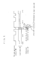
- table 1 is conducted by the 2 bit shift register 19 and the exclusive OR circuit 20 in the construction of figure 1, and after the transmission of PN code 2 is concluded, the data selector 21 is turned to the side of the exclusive OR circuit 20.
- the demodulation can be conducted by the prior art demodulator shown in figure 9, and then, the reproduced data 17 corresponding to the 0 or ⁇ phase is obtained at the output of the demodulator 10.
- Figure 4 shows a circuit which easily realizes the switching of logic.
- reference numeral 22 designates an input terminal for a PN code distinguishing signal which is "0" when the difference between the numbers of "1" and “0” in the PN code is 1 + 4 N and which is "1" when that is 3 + 4 N.
- Table 2 phase of PN code phase of next PN code data phase 0 0 1 ⁇ 1 0 0 1 0 0 0 1 1 ⁇
- system is defined as MSK or GMSK modulation system, but the system may be any of ⁇ /4 phase modulation system and the same effects as described above are obtained.
- the phase shift time is provided between the respective PN codes and 1 bit inserted in the phase shift time data period is shifted, but a plurality of bits in the phase shift time may be shifted.
- the final one bit or a plurality of bits at the final portion of the PN code may be replaced in accordance with the code which is to be modulated. Then, the data transmission efficiency can be further enhanced with the same effects as described above.
- FIG. 5 shows a second embodiment of the present invention.
- phase variation modulation is executed between the PN code data in the dispersion system utilizing the phase modulation, whereby multi-phase data are transmitted.
- reference numeral 1 designates an n bit data input terminal and reference numeral 23 designates a D/A converter.
- reference numeral 1 designates an n bit data input terminal and reference numeral 23 designates a D/A converter.
- the data period shown in figure 5 it is controlled such that the next data is phase shifted by 0, ⁇ /4, ⁇ /2, or 3 /4.
- Figure 7 shows waveforms of the respective portions of figure 5.
- the dispersion and the data modulation are conducted at the same time by phase shifting a predetermined bit inserted in the phase shift time data period provided between the PN codes or a predetermined bit at the latter half portion of PN code in accordance with the data to be modulated. Therefore, the apparatus can be constructed in a small size and at a low cost, and furthermore, dispersion outputs which are not deteriorated in the MSK or GMSK properties are obtained.
Landscapes
- Engineering & Computer Science (AREA)
- Computer Networks & Wireless Communication (AREA)
- Signal Processing (AREA)
- Digital Transmission Methods That Use Modulated Carrier Waves (AREA)
Applications Claiming Priority (2)
| Application Number | Priority Date | Filing Date | Title |
|---|---|---|---|
| JP63222757A JPH0748707B2 (ja) | 1988-09-06 | 1988-09-06 | 直接拡散変調装置 |
| JP222757/88 | 1988-09-06 |
Publications (3)
| Publication Number | Publication Date |
|---|---|
| EP0358466A2 true EP0358466A2 (de) | 1990-03-14 |
| EP0358466A3 EP0358466A3 (de) | 1991-03-27 |
| EP0358466B1 EP0358466B1 (de) | 1995-11-08 |
Family
ID=16787433
Family Applications (1)
| Application Number | Title | Priority Date | Filing Date |
|---|---|---|---|
| EP89308997A Expired - Lifetime EP0358466B1 (de) | 1988-09-06 | 1989-09-06 | "Direct-sequence"-Modulationsgerät |
Country Status (3)
| Country | Link |
|---|---|
| US (1) | US5020075A (de) |
| EP (1) | EP0358466B1 (de) |
| JP (1) | JPH0748707B2 (de) |
Cited By (3)
| Publication number | Priority date | Publication date | Assignee | Title |
|---|---|---|---|---|
| GB2333673A (en) * | 1998-01-21 | 1999-07-28 | Nokia Mobile Phones Ltd | Despreading a signal which has been spread by a code and modulated according to a non-linear modulation scheme |
| WO2001037504A1 (de) * | 1999-11-15 | 2001-05-25 | Infineon Technologies Ag | Verwendung eines auf frequenzmodulation basierenden transceivers für mit einem spreizspektrumverfahren kodierte signale |
| RU2841993C1 (ru) * | 2024-12-26 | 2025-06-18 | Акционерное общество "Всероссийский научно-исследовательский институт радиотехники" | Способ формирования сложного фазоманипулированного сигнала повышенной структурной скрытности |
Families Citing this family (17)
| Publication number | Priority date | Publication date | Assignee | Title |
|---|---|---|---|---|
| JP2803237B2 (ja) * | 1989-11-07 | 1998-09-24 | ダイキン工業株式会社 | データ伝送方法およびその装置 |
| JP2922707B2 (ja) * | 1992-03-06 | 1999-07-26 | 三菱電機株式会社 | 自動周波数制御方式 |
| US5454009A (en) * | 1994-01-13 | 1995-09-26 | Scientific-Atlanta, Inc. | Method and apparatus for providing energy dispersal using frequency diversity in a satellite communications system |
| US5748679A (en) * | 1995-04-28 | 1998-05-05 | Trw Inc. | Modulated clock MSK modulator for high data rate applications |
| US6826169B1 (en) * | 1996-12-20 | 2004-11-30 | Fujitsu Limited | Code multiplexing transmitting apparatus |
| US6094450A (en) * | 1997-06-20 | 2000-07-25 | Cincinnati Electronics Corporation | Spread spectrum chip shift keying modulation/demodulation system and method |
| US6246697B1 (en) * | 1998-01-24 | 2001-06-12 | Motorola, Inc. | Method and system for generating a complex pseudonoise sequence for processing a code division multiple access signal |
| US6459726B1 (en) * | 1998-04-24 | 2002-10-01 | Micron Technology, Inc. | Backscatter interrogators, communication systems and backscatter communication methods |
| US6611567B1 (en) * | 1999-01-29 | 2003-08-26 | Agere Systems, Inc. | Method and apparatus for pulse shaping |
| CA2539495A1 (en) * | 2003-10-29 | 2005-05-12 | Viasat, Inc. | Gmsk spread modulation |
| US7508884B2 (en) * | 2005-03-24 | 2009-03-24 | Harris Corporation | System and method for communicating data using constant amplitude equalized waveform |
| JP4110196B1 (ja) | 2007-07-24 | 2008-07-02 | 株式会社アドバンテスト | 波形発生装置、波形生成装置、試験装置およびプログラム |
| JP5118912B2 (ja) * | 2007-07-24 | 2013-01-16 | 株式会社アドバンテスト | 波形発生装置、波形生成装置、試験装置およびプログラム |
| JP4110197B1 (ja) | 2007-07-24 | 2008-07-02 | 株式会社アドバンテスト | 波形発生装置、波形生成装置、試験装置およびプログラム |
| JP5235078B2 (ja) * | 2008-02-01 | 2013-07-10 | 株式会社アドバンテスト | 波形発生装置、波形生成装置、試験装置およびプログラム |
| JP5485283B2 (ja) * | 2008-10-24 | 2014-05-07 | テレフオンアクチーボラゲット エル エム エリクソン(パブル) | 位相・振幅変調器 |
| CN103269236B (zh) * | 2013-05-24 | 2015-12-02 | 王红星 | 码元分组时移位置扩频调制和解调方法 |
Family Cites Families (9)
| Publication number | Priority date | Publication date | Assignee | Title |
|---|---|---|---|---|
| US4383322A (en) * | 1980-05-02 | 1983-05-10 | Harris Corporation | Combined use of PN sequence for data scrambling and frame synchronization in digital communication systems |
| US4383323A (en) * | 1980-06-09 | 1983-05-10 | Bell Telephone Laboratories, Incorporated | Spread spectrum FH-MFSK transmitter and receiver |
| US4355399A (en) * | 1981-02-23 | 1982-10-19 | Bell Telephone Laboratories, Incorporated | Adaptive spread spectrum FH-MFSK transmitter and receiver |
| US4527275A (en) * | 1982-02-12 | 1985-07-02 | Arinc Research Corporation | Correlation data communications system |
| JPS5933962A (ja) * | 1982-08-20 | 1984-02-24 | Oki Electric Ind Co Ltd | デイジタルmsk変調器 |
| US4581749A (en) * | 1984-07-02 | 1986-04-08 | Motorola, Inc. | Data frequency modulator with deviation control |
| JPS6167353A (ja) * | 1984-09-10 | 1986-04-07 | Omron Tateisi Electronics Co | Msk方式変調回路 |
| US4648099A (en) * | 1984-12-17 | 1987-03-03 | Allied Corporation | Digital minimum shift keyed modulator |
| IT1206820B (it) * | 1987-06-26 | 1989-05-03 | Selenia Spazio Spa | Modem "spread spectrum" digitale a sequenza diretta |
-
1988
- 1988-09-06 JP JP63222757A patent/JPH0748707B2/ja not_active Expired - Fee Related
-
1989
- 1989-09-05 US US07/402,882 patent/US5020075A/en not_active Expired - Lifetime
- 1989-09-06 EP EP89308997A patent/EP0358466B1/de not_active Expired - Lifetime
Cited By (3)
| Publication number | Priority date | Publication date | Assignee | Title |
|---|---|---|---|---|
| GB2333673A (en) * | 1998-01-21 | 1999-07-28 | Nokia Mobile Phones Ltd | Despreading a signal which has been spread by a code and modulated according to a non-linear modulation scheme |
| WO2001037504A1 (de) * | 1999-11-15 | 2001-05-25 | Infineon Technologies Ag | Verwendung eines auf frequenzmodulation basierenden transceivers für mit einem spreizspektrumverfahren kodierte signale |
| RU2841993C1 (ru) * | 2024-12-26 | 2025-06-18 | Акционерное общество "Всероссийский научно-исследовательский институт радиотехники" | Способ формирования сложного фазоманипулированного сигнала повышенной структурной скрытности |
Also Published As
| Publication number | Publication date |
|---|---|
| JPH0748707B2 (ja) | 1995-05-24 |
| US5020075A (en) | 1991-05-28 |
| EP0358466A3 (de) | 1991-03-27 |
| JPH0270136A (ja) | 1990-03-09 |
| EP0358466B1 (de) | 1995-11-08 |
Similar Documents
| Publication | Publication Date | Title |
|---|---|---|
| EP0358466A2 (de) | "Direct-sequence"-Modulationsgerät | |
| US6865236B1 (en) | Apparatus, and associated method, for coding and decoding multi-dimensional biorthogonal codes | |
| EP0400027B1 (de) | Vorrichtung und verfahren zur modulierung in quadratur | |
| KR900008412B1 (ko) | 주파수 검파기 | |
| US6363100B1 (en) | Radio data communication system using spread spectrum scheme | |
| US5812612A (en) | Method and apparatus for transmitting an intermittent signal in a ratio communication system | |
| EP0881806B1 (de) | Rahmenstruktur mit einer Mehrzahl von Modulationsarten | |
| US3984777A (en) | Carrier wave reproducer device for use in the reception of a multi-phase phase-modulated wave | |
| US7065157B2 (en) | GMSK modulation techniques | |
| KR100231876B1 (ko) | 정진폭특성을 갖는 직교진폭변조방법 및 그 장치 | |
| JP3307217B2 (ja) | スペクトラム拡散通信方式における受信装置 | |
| EP0480674A2 (de) | Modulator für binäre Phasensprungmodulation | |
| US7242663B2 (en) | Multi-channel spread spectrum communications system | |
| US7324581B2 (en) | Apparatus for mapping and spreading data symbols in mobile communication system | |
| US6310870B1 (en) | Method for transmitting high data rate information in code division multiple access systems | |
| US4881246A (en) | Method and apparatus for demodulating a class of M-ary phase shift keyed (PSK) signals | |
| US4499585A (en) | Method and apparatus for producing a shaped spectrum modulating signal | |
| US6389081B1 (en) | Signal transmission equipment | |
| US5295160A (en) | Apparatus for FM-modulation of digital signals | |
| KR950003669B1 (ko) | 4위상 차분 직교위상쉬프트키잉 변복조기 | |
| JPH0225306B2 (de) | ||
| US6496542B1 (en) | Digital communication system | |
| JPH05110538A (ja) | スペクトル拡散通信装置 | |
| EP0765545A2 (de) | Kommunikationssystem und übertragungsvorrichtung hierzu | |
| JPH06232838A (ja) | スペクトラム拡散送受信機 |
Legal Events
| Date | Code | Title | Description |
|---|---|---|---|
| PUAI | Public reference made under article 153(3) epc to a published international application that has entered the european phase |
Free format text: ORIGINAL CODE: 0009012 |
|
| AK | Designated contracting states |
Kind code of ref document: A2 Designated state(s): FR GB NL |
|
| PUAL | Search report despatched |
Free format text: ORIGINAL CODE: 0009013 |
|
| 17P | Request for examination filed |
Effective date: 19901228 |
|
| AK | Designated contracting states |
Kind code of ref document: A3 Designated state(s): FR GB NL |
|
| 17Q | First examination report despatched |
Effective date: 19930709 |
|
| GRAA | (expected) grant |
Free format text: ORIGINAL CODE: 0009210 |
|
| AK | Designated contracting states |
Kind code of ref document: B1 Designated state(s): FR GB NL |
|
| ET | Fr: translation filed | ||
| PLBE | No opposition filed within time limit |
Free format text: ORIGINAL CODE: 0009261 |
|
| STAA | Information on the status of an ep patent application or granted ep patent |
Free format text: STATUS: NO OPPOSITION FILED WITHIN TIME LIMIT |
|
| 26N | No opposition filed | ||
| REG | Reference to a national code |
Ref country code: FR Ref legal event code: D6 |
|
| REG | Reference to a national code |
Ref country code: GB Ref legal event code: IF02 |
|
| PGFP | Annual fee paid to national office [announced via postgrant information from national office to epo] |
Ref country code: FR Payment date: 20050823 Year of fee payment: 17 |
|
| PGFP | Annual fee paid to national office [announced via postgrant information from national office to epo] |
Ref country code: GB Payment date: 20050831 Year of fee payment: 17 |
|
| PGFP | Annual fee paid to national office [announced via postgrant information from national office to epo] |
Ref country code: NL Payment date: 20050915 Year of fee payment: 17 |
|
| PG25 | Lapsed in a contracting state [announced via postgrant information from national office to epo] |
Ref country code: NL Free format text: LAPSE BECAUSE OF NON-PAYMENT OF DUE FEES Effective date: 20070401 |
|
| GBPC | Gb: european patent ceased through non-payment of renewal fee |
Effective date: 20060906 |
|
| NLV4 | Nl: lapsed or anulled due to non-payment of the annual fee |
Effective date: 20070401 |
|
| REG | Reference to a national code |
Ref country code: FR Ref legal event code: ST Effective date: 20070531 |
|
| PG25 | Lapsed in a contracting state [announced via postgrant information from national office to epo] |
Ref country code: GB Free format text: LAPSE BECAUSE OF NON-PAYMENT OF DUE FEES Effective date: 20060906 |
|
| PG25 | Lapsed in a contracting state [announced via postgrant information from national office to epo] |
Ref country code: FR Free format text: LAPSE BECAUSE OF NON-PAYMENT OF DUE FEES Effective date: 20061002 |