EP0355797B1 - Signalisierungsgerät zur Verwendung in einem ATM-Vermittlungssystem - Google Patents
Signalisierungsgerät zur Verwendung in einem ATM-Vermittlungssystem Download PDFInfo
- Publication number
- EP0355797B1 EP0355797B1 EP89115476A EP89115476A EP0355797B1 EP 0355797 B1 EP0355797 B1 EP 0355797B1 EP 89115476 A EP89115476 A EP 89115476A EP 89115476 A EP89115476 A EP 89115476A EP 0355797 B1 EP0355797 B1 EP 0355797B1
- Authority
- EP
- European Patent Office
- Prior art keywords
- signalling
- data
- line
- switching means
- frame
- Prior art date
- Legal status (The legal status is an assumption and is not a legal conclusion. Google has not performed a legal analysis and makes no representation as to the accuracy of the status listed.)
- Expired - Lifetime
Links
Images


Classifications
-
- H—ELECTRICITY
- H04—ELECTRIC COMMUNICATION TECHNIQUE
- H04Q—SELECTING
- H04Q11/00—Selecting arrangements for multiplex systems
- H04Q11/04—Selecting arrangements for multiplex systems for time-division multiplexing
- H04Q11/0428—Integrated services digital network, i.e. systems for transmission of different types of digitised signals, e.g. speech, data, telecentral, television signals
- H04Q11/0478—Provisions for broadband connections
-
- H—ELECTRICITY
- H04—ELECTRIC COMMUNICATION TECHNIQUE
- H04L—TRANSMISSION OF DIGITAL INFORMATION, e.g. TELEGRAPHIC COMMUNICATION
- H04L49/00—Packet switching elements
- H04L49/30—Peripheral units, e.g. input or output ports
-
- H—ELECTRICITY
- H04—ELECTRIC COMMUNICATION TECHNIQUE
- H04L—TRANSMISSION OF DIGITAL INFORMATION, e.g. TELEGRAPHIC COMMUNICATION
- H04L49/00—Packet switching elements
- H04L49/30—Peripheral units, e.g. input or output ports
- H04L49/3009—Header conversion, routing tables or routing tags
-
- H—ELECTRICITY
- H04—ELECTRIC COMMUNICATION TECHNIQUE
- H04L—TRANSMISSION OF DIGITAL INFORMATION, e.g. TELEGRAPHIC COMMUNICATION
- H04L12/00—Data switching networks
- H04L12/54—Store-and-forward switching systems
- H04L12/56—Packet switching systems
- H04L12/5601—Transfer mode dependent, e.g. ATM
- H04L2012/5629—Admission control
- H04L2012/563—Signalling, e.g. protocols, reference model
-
- H—ELECTRICITY
- H04—ELECTRIC COMMUNICATION TECHNIQUE
- H04Q—SELECTING
- H04Q2213/00—Indexing scheme relating to selecting arrangements in general and for multiplex systems
- H04Q2213/107—Control equipment for part of the connection
-
- H—ELECTRICITY
- H04—ELECTRIC COMMUNICATION TECHNIQUE
- H04Q—SELECTING
- H04Q2213/00—Indexing scheme relating to selecting arrangements in general and for multiplex systems
- H04Q2213/29—ATM
Definitions
- the present invention relates generally to a broadband communication system, and more particularly to a signalling apparatus in an ATM (Asynchronous Transfer Mode) switching system.
- ATM Asynchronous Transfer Mode
- An ISDN Integrated Services Digital Network
- information channels or B or H channels
- signalling channels or "D channels"
- a layered data processing scheme utilizes a three layer structure.
- layers 2 functions commonly accomplished by LAPD (Link Access Procedure on the D-channel) devices are accomplished.
- LAPD Link Access Procedure on the D-channel
- call control in accordance with the 1.451 standard is accomplished.
- signalling channels from a plurality of subscriber lines are separated from information channels. Only the signalling channels are multiplexed and guided to a signalling processor. Thereafter, the processes of layer 2 (LAPD) and layer 3 (call control) are performed. See for example, Fig. 12 of "Signalling Processing in an I-Interface Switching System", IEICE (The Institute of Electronics Information and Communication Engineers) Technical Report SE 87-85, or Japanese Laid-Open Patent Application No. 131652/1987.
- the International Telegraph and Telephone Consultative Committee (“CCITT”) is now considering a "broadband ISDN" as the next generation ISDN.
- the broadband ISDN is an attempt to provide switching services at a line rate of, for example, 150 Mbit/s.
- CCITT Draft Recommendation 1.121 cites the ATM (Asynchronous Transfer Mode) as a favourable means for implementing the above-mentioned broadband ISDN.
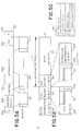
- the ATM switching system is a system in which all data, including control signals and information, are transferred in fixed-length packets called "cells". For example, when a signalling frame 50 is to be transmitted from a subscriber's terminal, as shown in Fig. 5 A, the frame 50 is segmented into fixed length cells 51A - 51 N, which cells are then transmitted through the subscriber line. An ADP processing unit 100 in the switching system will then reassemble the signal frame 50 from the cells 51A- 51 N received thereby, and LAPD-LSI 101 performs layer 2 functions for a signalling channel (which is called "LAPD"). Signalling rocessor 40 processes functions of layer 3 for a signalling channel (which is called "call control"). When, on the other hand, a signal frame is to be transmitted from the switching system to a subscriber terminal, the switching system will perform such segmenting and the subscriber terminal will perform such a reassembly procedure.
- LAPD signalling channel
- ADP processing unit The processing unit of the adaptation layer, including the segmenting/reassembling processes, is hereinafter called "ADP processing unit.”
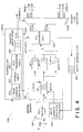
- 11 designates optical fibres having a transmission rate of, for example, about 150 Mbit/s
- 10 designates subscriber line interfaces which perform, for example, optical/electrical signal conversion
- 30 designates an ATM switch for switching cells
- 12 (12-1 -12- j) designates 8-bit buses.
- Cell dropper/inserter circuits 16 (16-1 - 16-j) are inserted between the subscriber line interfaces 10 and the ATM switch 30. In receiving subsystems (from the subscriber line interfaces 10 to the ATM switch 30), only cells in the signalling channels are separated and extracted, while in transmission subsystems (from the ATM switch 30 to the subscriber line interfaces 10), signalling channel cells are inserted.
- Cell data from the cell dropper/inserter 16 is multiplexed by a multiplexer/demultiplexer (MUX) 17, and connected to a subscriber line signalling unit 1 via a bus 19.
- MUX multiplexer/demultiplexer
- the subscriber line signalling unit 1 comprises: a multiplexer/demultiplexer (MUX) 18, for multiplexing and demultiplexing cell data for each subscriber's line; the above-mentioned ADP processing units 100 (100-1 - 100-j); LAPD-LSI 101 (101-1 101-j), for processing layer 2 signalling channels; and a bus 103.
- MUX multiplexer/demultiplexer
- a broadband communication system in accordance with the invention is defined by claim 1.
- a method, in accordance with the invention, for communicating signalling channel data cells with a subscriber line signalling apparatus in a broadband communication system is defined by claim 10.
- signalling channel data packets for cells are routed (i.e. collected and distributed) to a signalling apparatus using the ATM switch, and the signalling apparatus can perform an adaptation process commonly for a plurality of (subscriber) lines.
- An advantage of the present invention is that the equipment requirements are minimised, because none of the cell dropper/inserters and cell multiplex- er/demultiplexers of Fig. 9 is necessary. Also, since the adaptation process can be performed commonly, the amount of hardware necessary for the adaptation process can be reduced. Thus, the system of the invention provides reduced cost, smaller size, and increased reliability.
- the signalling apparatus comprises a trunk line signalling apparatus working in concert with a subscriber line signalling apparatus.
- a subscriber line signalling apparatus 1 includes an ADP processing unit 100 for performing an adaptation process, including segmentation of a communication frame and reassembly of received cells.
- LAPD-LSI's 101 (101-1 - 101-1) for performing layer 2 protocol processing of a signalling channel.
- This apparatus 1 connected, via a bus 15, to an ATM switch 30.
- the subscriber line signalling apparatus 1 is connected, via a bus 103, to a processor 40 for performing, for example, the operation of layer 3 protocol processing of signalling channels, and controlling of the LAPD-LSI's and initializing of an ATM switch.
- Numeral 11 designates optical fibres, or the like, having a transmission rate of, for example, about 150 Mbits/s.
- Numeral 14 designates optical fibres having a transmission rate of, for example, about 150 Mbits/s or 600 Mbits/s.
- the components referenced by numerals 12 (12-1 - 12-j), 13 (13-1 - -13- k) and 15 are suitably formed of eight-bit wide buses.
- Subscriber line interfaces 10 and trunk line interfaces 20 suitably perform optical/electrical signal conversion, and add/delete a route information segment to and from individual cells, respectively.
- optical fibres 11, 14 and the buses 12 and 13 are illustrated as a single line in Fig. 1, each of these fibres and buses is fabricated from a pair of transmission and reception lines or buses.
- the number of LAPD-LSI's may be reduced (j>I) or additional LAPD-LSI's may be provided (j ⁇ I) to provide against emergencies.
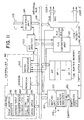
- Fig. 2 shows a system in which the process of layer 2 of signalling channels for a plurality of subscriber lines (11-1 - 11-j) is performed by a single LAPD-LSI 101.
- Fig. 3 is a block diagram showing the transmission system in the above-mentioned ADP processing unit 100
- Fig. 4 is a block diagram of the receiving system in the ADP processing unit 100.
- Each cell. 51 comprises 36 bytes, and consists of a cell header 52 of 4 bytes and an information field 53 of 32 bytes.
- the cell header 52 includes a first 12 bits 520 which form a VCN (Virtual Channel Number) field for identification of the cell, a reserved field 521 and an HCS (Header Check Sequence) field 522 for detecting cell header abnormalities.
- VCN Virtual Channel Number
- HCS Header Check Sequence
- the route information field 56 at the beginning of the cell of Fig. 5 B is applied thereto only within the ATM switching system, and each cell is otherwise transmitted in a format lacking the above-mentioned route information field 56 through the subscriber lines 11 or through the trunk lines 14.
- the route information field is used to store therein information specifying the output line to which a cell switched in the ATM switch 30 should be transmitted, and the subscriber line number, etc.
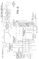
- a transmission line selector 110A has signal line sets 102A(102A-1 - 102A-1), each of which consist of three lines, namely, a transmission data (TXD), transmission clock (TXC) and echo (E) lines, and each of which is connected to a corresponding one of LAPD-LSI's 101 (101-1 - 101-i); the selector 110A has a function of collision control to extract only the frame on a specified line when a plurality of frames are simultaneously transmitted from a plurality of LAPD's.
- the D-channel access procedure described in the CCITT Recommendation 1.430, may be used as the procedure of the collision control.
- the line number selected in accordance with the collision control is communicated to a CTL 190, while transmission data is transmitted to a frame detector 112.
- the transmission line selector 110A is necessary only in the first embodiment of the present invention.
- the frame detector 112 will communicate the DLCI (Data Link Connection Identifier) in the address field 50B of the frame to the CTL 190, and will arrange the data from the address field to FCS (Frame Check Sequence) field 50E into an 8-bit parallel data after deleting a '0' bit for flag identification, and transmit it to a counter 116. If the data is the last data of a frame, then such fact is communicated to the counter 116 through a final notice signal line.
- DLCI Data Link Connection Identifier
- the counter 116 will transfer the frame data to a FIFO-A 120.
- the cell type 542 and the effective information length 543 shown in the ADP header format of Fig. 5 B are communicated to the CTL 190, and thereafter it will transfer data from the frame detector 112 to a FIFO-B 121.
- the counter 116 will likewise communicate the cell type and the effective information length to the CTL 190, and will transfer subsequent data to the FIFO-A 120. In the manner as described, the FIFO-A and FIFO-B are alternately used.
- the CTL 190 is constituted by, for example, ⁇ CPU's, ROM's and RAM's, and contains a DLCI/header corresponding table 191, in which contents of headers (all of the 10 bytes from the route information 56 to the ADP header 54 in Fig. 5 B ) corresponding to the combinations of line numbers and DLCI are set from outside via control bus 103.
- the CTL 190 will search the DLCI/header corresponding table 191 upon receiving the communication of the line number and the DLCI, and write the contents of the corresponding table onto a header register 118.
- the unique DLCI is converted, using a DLCI conversion table 195, into a DLCI which is actually transmitted to a subscriber device. Subsequently, upon receipt of the communication of the cell type and effective information length from the counter 116, a corresponding register, within a header register 118, is rewritten in accordance with an ADP header format 54 of Fig. 5 B and a selector (SEL) 122 is activated.
- SEL selector
- the SEL 122 will first transmit the data in a header register 118, and will next transmit the data in the FIFO-A 120, thereby completing the transmission of the cell. Subsequently, when receiving an activation from the CTL, the SEL 122 will transmit the data in the header register 118, and will then transmit the data in the FIFO-B 121, thereby completing the transmission of the cell. Subsequently, the SEL 122 will transmit the data in the FIFO-A and the data in the FIFO-B alternately.
- an amount to be processed for forming a header for the transmission of a cell can be reduced by arranging such that the searching of the DLCI/header corresponding table 191 and the setting of the ADP header in the header register are performed separately in the CTL and a reading of the data in the header register 118 will not change such data.
- a cell writing unit 124 is connected with the ATM switch 30 through a receiving bus 15B for receiving cells of a signalling channel from a subscriber unit.
- the received cell data is transferred to an empty area of a first buffer BF in a buffer memory 126 according to an address indicated by a WA (Write Address) register 125 within the cell writer 124.
- WA Write Address
- the data in an empty address FIFO 130 is set in the WA 125 for preparation for receiving the next cell.
- the buffer memory 126 comprises:the first buffer BF of the form of a FIFO for receiving and temporarily storing therein cells arriving there at a rate of, for example, 150 Mbit/s; and second buffers BF-I - BF-n of a FIFO form prepared for respective combinations of line.numbers and VCN in cell headers for the subsequent reassembling process.
- the construction of the BF of the form of FIFO, the manner of using a chain pointer, and the mannerof using theWAregister 125, RA (Read Address) register 192, and the empty address FIFO 130 are described in the previously mentioned literature "A Memory Switch Architecture for ATM Switching Network".
- a CTL 190 has an RA register 192 which corresponds to the first buffer BF, and will check the line number, the VCN in the cell header and the cell type in the ADP header among the contents of the cell of the address indicated by the RA, and will first transfer such cell data to a second buffer BF-i which has the combination of the corresponding line number and VCN.
- a second buffer BF-i which has the combination of the corresponding line number and VCN.
- an actual data transfer from memory to memory is not performed but transfer is performed only by rewriting a second buffer address table 193 provided in the CTL 190 and further rewriting the buffer chain pointer.
- the CTL 190 will activate a P/S unit 128 in accordance with the data in the transfer order storing FIFO 194 and at the same time specify an output line number to a receipt line selector 110B.
- a unique DLCI is derived, using a DLCI conversion table 195, from the DLCI from a subscriber unit, and the unique DLCI is simultaneously communicated to the P/S unit.
- the P/S unit 128 will read the data of the specified address in response to an activation from the CTL 190, and will convert data other than the header field into a serial data and will transfer such data to the receipt line selector 110B after insertion thereto of "0" and adding a frame delimiting cell type flag 50A, 50F thereto. In the second embodiment of the present invention, conversion into a unique DLCI is also performed.
- the receipt line selector 110B is connected with LAPD-LSI 101 (101-1 - 101-j), via signal line sets 102B 102B-1 - 102B-I), each of which consists of two lines, namely, a receipt data line (RxD) and a receipt clock (RxC), and has a function of transmitting data only to a signal line having a line number specified by the CTL 190.
- the receipt line selector 110B is, as is the transmission line selector shown in Fig. 3, necessitated only in the arrangement of the first embodiment and not necessary in the arrangement of the second embodiment.
- the above embodiments are arranged to control each hardware in the ADP processing unit by means of the CTL unit 190 which uses a wCPU, it is also possible to increase the processing rate by implementation of all the functions of the CTL by hardware.
- the first buffer BF for rate adaptation may be omitted, and the contents of the header may be checked in the cell writer and the cell data may be directly transferred to the second buffers BF-I - BF-n.
- the arrangement may be such that the subscriber line number is not recorded, and the VCN of the cell is converted in the subscriber line interface 10 into a VCN unique to the VCN used for subscriber lines 1 ... j. Further, where the management of DLCI is performed for each subscriber line separately from the others, different subscribers can simultaneously use the same DLCI. Then, in accordance with the arrangement of the second embodiment (Fig. 2), wherein a LAPD-LSI is provided common to a plurality of subscriber lines, two or more links having the same DLCI for different subscribers cannot be discriminated.
- links can be normally discriminated if the arrangement is such that a DLCI conversion table is provided in the ADP processing unit 100 and, between the LAPD-LSI 101 and the ADP processing unit 100, unique DLCI's are used for the subscriber lines 1 ... j.
- the subscriber line interface 10-i communicates route information 56 from each cell 51 inputted from the ATM switch 30 through reception bus 12A, a parallel/serial (P/S) converter 202 for converting parallel data of the input cell which has no route information to bit serial data, and electrical/opt- ical (E/O) signal converter 203 for converting the bit serial data to optical signals.
- P/S parallel/serial
- E/O electrical/opt- ical
- the subscriber line interface 10-i further comprises an optical/electrical (O/E) signal converter 204 for converting optical signals transmitted from a subscriber terminal onto a transmission optical fibre 11 B to bit serial electrical signals, a serial/parallel (S/P) converter 205 for converting the bit serial signal to 8- bit parallel data, a header separator circuit 206, a header inserter circuit 207, and a header conversion table memory 208.
- O/E optical/electrical
- S/P serial/parallel
- each cell transmitted from the subscriber terminal includes a cell header 52 and an information field 53 as shown in Fig. 5B.
- the header separator circuit 206 operates to separate the cell header 52 from the received cell in order to access the header conversion table 208 in accordance with the value of field VCN extracted from the header, and to provide the information field 53 of the received cell to the header inserter circuit 207.
- the header conversion table memory 208 stores a plurality of records, each of which comprises route information 56, and a new header 52 including a new VCN 520 as shown in Fig. 7. One of these records is read out to the header inserter circuit 207 by addressing in accordance with the extracted VCN.
- the header inserter circuit 207 operates to output a header converted cell which has a route information field 56 and a new cell header 52 onto a transmission bus 12B.
- VCN If an input (extracted) VCN has a value corresponding to the signalling channel, a record which includes route information to designate the bus 15 as an output port is read out. If the input VCN corresponds to an information channel, a record which designates one of output buses 13-1 through 13-k is read out.
- the contents of the header conversion table memory 208 are prepared by the processor 40 through a bus 104.
- Fig. 8 shows a third embodiment of the present invention.
- a signalling control system the same as that which is adopted in the first or second embodiment, is also applied to the trunk line signal processing.
- a trunk line signalling apparatus 2 has substantially the same construction as the line signalling apparatus shown in Figs. 1 or 2.
- Fig. 8 signalling channel cells transmitted from the subscriber terminal are relayed to the bus 15 by the ATM switch 30.
- a reassembly process from cell(s) to a frame and the layer 2 process are performed by the subscriber line signalling apparatus, whereby a signalling channel message extracted from the reassembled frame is supplied to the processor 40.
- Each trunk line interface (20-1 - 20-k) may have the same construction as the subscriber line interface shown in Fig. 6.
- signalling channel cells transmitted from another ATM switch through one of the optical fibres 14-1 through 14-k are relayed to a bus 25 by the ATM switch 30 and inputted to the trunk line signalling apparatus 2.
- the trunk line signalling apparatus 2 performs the reassembling from the received cells to a frame and the level 2 process, so that a signalling channel message extracted from the reassembled frame is also supplied to the processor40.
- the processor 40 performs a layer 3 process as to the signalling channel message supplied from the signalling apparatuses 1 and 2. As a result, if it is necessary to transmit a new signalling channel message to another ATM switch, the processor40 suitably communicates a request for transmitting the new message to the trunk line signalling apparatus.
- the trunk line signalling apparatus performs the layer 2 processing and the segmenting process as to the new message, and sends out a series of new cells thus produced to the ATM switch 30 through the bus 25.
- These cells are relayed to one of the trunk line buses 13-1 through 13-k according to their route information which is added by the ADP processing unit in the trunk line signalling apparatus.
- Each of the trunk line interfaces 20-1 through 20- k is provided with a header conversion table memory namely as the subscriber line interface 10-i shown in Fig. 6.
- the contents of the table are also managed by the processor via a bus line 105.
- an ADP processing unit is provided common to the subscriber lines, whereby advantages can be achieved in that the cell dropper/inserters, one for each subscriber line, buses for line collection/distribution or multiplexer/demulti- plexers necessitated in a subscriber line signalling apparatus constructed in a similar manner to prior art ISDN switching systems, can be omitted and the ADP processing units can be reduced in number, so that the amount of hardware can be reduced.
- Figs. 10 and 11 are examples of an actual construction for the transmitting subsystem of Fig. 3 and the receiving subsystem of Fig. 4, of the ADP processing unit, respectively.
- Fig. 12 shows an ATM switching network and layer model of an ATM terminal and an ATM switching system.
Landscapes
- Engineering & Computer Science (AREA)
- Computer Networks & Wireless Communication (AREA)
- Signal Processing (AREA)
- Data Exchanges In Wide-Area Networks (AREA)
- Communication Control (AREA)
Claims (12)
Applications Claiming Priority (3)
| Application Number | Priority Date | Filing Date | Title |
|---|---|---|---|
| JP21071888 | 1988-08-26 | ||
| JP210718/88 | 1988-08-26 | ||
| JP21071888 | 1988-08-26 |
Publications (4)
| Publication Number | Publication Date |
|---|---|
| EP0355797A2 EP0355797A2 (de) | 1990-02-28 |
| EP0355797A3 EP0355797A3 (de) | 1991-02-06 |
| EP0355797B1 true EP0355797B1 (de) | 1995-03-15 |
| EP0355797B2 EP0355797B2 (de) | 2001-03-21 |
Family
ID=16593951
Family Applications (1)
| Application Number | Title | Priority Date | Filing Date |
|---|---|---|---|
| EP89115476A Expired - Lifetime EP0355797B2 (de) | 1988-08-26 | 1989-08-22 | Signalisierungsgerät zur Verwendung in einem ATM-Vermittlungssystem |
Country Status (3)
| Country | Link |
|---|---|
| EP (1) | EP0355797B2 (de) |
| JP (2) | JP3132564B2 (de) |
| DE (1) | DE68921685T3 (de) |
Families Citing this family (15)
| Publication number | Priority date | Publication date | Assignee | Title |
|---|---|---|---|---|
| JPH02228838A (ja) * | 1989-03-02 | 1990-09-11 | Oki Electric Ind Co Ltd | インターフェース回路 |
| FR2659513A1 (fr) * | 1990-03-12 | 1991-09-13 | Cit Alcatel | Installation terminale d'abonne pour reseau asynchrone. |
| JPH0477148A (ja) * | 1990-07-17 | 1992-03-11 | Fujitsu Ltd | シグナリング・データ受信処理方式 |
| CA2049428C (en) * | 1990-08-20 | 1996-06-18 | Yasuro Shobatake | Atm communication system |
| FR2670974A1 (fr) * | 1990-12-20 | 1992-06-26 | Lmt Radio Professionelle | Dispositif pour la transmission par un reseau asynchrone, notamment un reseau de type atm, de donnees de signalisation voie par voie regroupees dans une multitrame emise de maniere synchrone en mode hors bande. |
| JP2938611B2 (ja) * | 1991-05-14 | 1999-08-23 | 富士通株式会社 | テレビ信号交換方式 |
| JPH0548638A (ja) * | 1991-08-15 | 1993-02-26 | Fujitsu Ltd | Atm網におけるエンド・エンド間輻輳対処制御処理方式 |
| EP0531599B1 (de) * | 1991-09-13 | 1998-07-22 | International Business Machines Corporation | Konfigurierbare gigabit/s Vermittlunganpassungseinrichtung |
| US5396490A (en) * | 1992-03-23 | 1995-03-07 | Motorola, Inc. | Packet reassembly method and apparatus |
| DE59209115D1 (de) * | 1992-08-28 | 1998-02-12 | Siemens Ag | Verfahren und Schaltungsanordnung zum Übertragen von Nachrichtenzellen innerhalb eines ATM-Netzes |
| JP2577524B2 (ja) * | 1993-07-13 | 1997-02-05 | 日本電気株式会社 | セル交換機 |
| FR2707820B1 (fr) * | 1993-07-15 | 1995-08-18 | Cit Alcatel | Circuit d'interface de liaison numérique pour unité terminale de centre de commutation à mode de transfert asynchrone. |
| US5613069A (en) * | 1994-12-16 | 1997-03-18 | Tony Walker | Non-blocking packet switching network with dynamic routing codes having incoming packets diverted and temporarily stored in processor inputs when network ouput is not available |
| JPH1032584A (ja) * | 1996-07-17 | 1998-02-03 | Matsushita Electric Ind Co Ltd | 再送制御機能を有するデータ転送装置 |
| FI104601B (fi) * | 1997-06-27 | 2000-02-29 | Nokia Networks Oy | Signalointisanomien käsittely ATM-solmussa |
Citations (1)
| Publication number | Priority date | Publication date | Assignee | Title |
|---|---|---|---|---|
| EP0183592A1 (de) * | 1984-11-08 | 1986-06-04 | LABORATOIRE CENTRAL DE TELECOMMUNICATIONS Société anonyme: | Asynchrone Paketvermittlung |
Family Cites Families (3)
| Publication number | Priority date | Publication date | Assignee | Title |
|---|---|---|---|---|
| US4491945A (en) * | 1982-06-25 | 1985-01-01 | At&T Bell Laboratories | Fast packet switch |
| US4611322A (en) † | 1984-08-03 | 1986-09-09 | At&T Bell Laboratories | Traffic load control arrangement and method for a packet switching system |
| US4763317A (en) * | 1985-12-13 | 1988-08-09 | American Telephone And Telegraph Company, At&T Bell Laboratories | Digital communication network architecture for providing universal information services |
-
1989
- 1989-06-21 JP JP15677289A patent/JP3132564B2/ja not_active Expired - Lifetime
- 1989-08-22 DE DE68921685T patent/DE68921685T3/de not_active Expired - Fee Related
- 1989-08-22 EP EP89115476A patent/EP0355797B2/de not_active Expired - Lifetime
-
2000
- 2000-05-12 JP JP2000144585A patent/JP2000349790A/ja active Pending
Patent Citations (1)
| Publication number | Priority date | Publication date | Assignee | Title |
|---|---|---|---|---|
| EP0183592A1 (de) * | 1984-11-08 | 1986-06-04 | LABORATOIRE CENTRAL DE TELECOMMUNICATIONS Société anonyme: | Asynchrone Paketvermittlung |
Also Published As
| Publication number | Publication date |
|---|---|
| JP2000349790A (ja) | 2000-12-15 |
| DE68921685T3 (de) | 2001-06-13 |
| JPH02140037A (ja) | 1990-05-29 |
| JP3132564B2 (ja) | 2001-02-05 |
| EP0355797B2 (de) | 2001-03-21 |
| EP0355797A2 (de) | 1990-02-28 |
| DE68921685T2 (de) | 1995-07-27 |
| DE68921685D1 (de) | 1995-04-20 |
| EP0355797A3 (de) | 1991-02-06 |
Similar Documents
| Publication | Publication Date | Title |
|---|---|---|
| US5101404A (en) | Signalling apparatus for use in an ATM switching system | |
| US5303236A (en) | Signalling apparatus for use in an ATM switching system | |
| EP0942621B1 (de) | Multiprozessorsystem und Verfahren zur Zusammensetzung von ATM Zellen | |
| EP0406842B1 (de) | Paketvermittlungsnetzwerk für Kommunikation mit Verwendung von Paketen mit virtueller Verbindungserkennung VCI | |
| US5214642A (en) | ATM switching system and adaptation processing apparatus | |
| EP0858240B1 (de) | Anlage zur Zellenzusammensetzung und Multiplexierung, und Anlage zur Demultiplexierung | |
| US6031838A (en) | ATM switching system | |
| EP0355797B1 (de) | Signalisierungsgerät zur Verwendung in einem ATM-Vermittlungssystem | |
| EP1422891A2 (de) | ATM Vermittlungssystem | |
| JPH08186579A (ja) | 交換機アダプタ及び計算機及びデータ交換方法 | |
| GB2305084A (en) | Control of simultaneously-occurring messages in communications systems. | |
| US6628659B1 (en) | ATM cell switching system | |
| JP3184964B2 (ja) | 交換システムのatmセル変換方法 | |
| JP3146054B2 (ja) | Atm通信装置およびセル帯域管理方法 | |
| JPH0522403A (ja) | Stm−atm相互変換制御方式 | |
| JP3055547B2 (ja) | セル組立方法、セル分解方法、およびatmセル通信装置 | |
| JP3055548B2 (ja) | Atm通信装置 | |
| JP3129300B2 (ja) | Atm交換機 | |
| JP3129301B2 (ja) | Atm交換機 | |
| JP2785005B2 (ja) | Fc/atm網相互変換装置における多重/分離方式 | |
| JP2580744B2 (ja) | フレーム・リレー形データ交換機 | |
| WO1990016121A1 (en) | Data switching nodes | |
| JP2785006B2 (ja) | Fc/atm網相互変換装置における多重/分離方式 | |
| JP3014619B2 (ja) | 非同期転送モード通信システムおよびそのセル分解装置ならびに非同期転送モード通信方式 | |
| JPH1146200A (ja) | Atm交換機 |
Legal Events
| Date | Code | Title | Description |
|---|---|---|---|
| PUAI | Public reference made under article 153(3) epc to a published international application that has entered the european phase |
Free format text: ORIGINAL CODE: 0009012 |
|
| AK | Designated contracting states |
Kind code of ref document: A2 Designated state(s): DE FR GB |
|
| PUAL | Search report despatched |
Free format text: ORIGINAL CODE: 0009013 |
|
| 17P | Request for examination filed |
Effective date: 19901212 |
|
| AK | Designated contracting states |
Kind code of ref document: A3 Designated state(s): DE FR GB |
|
| RHK1 | Main classification (correction) |
Ipc: H04Q 11/04 |
|
| 17Q | First examination report despatched |
Effective date: 19930906 |
|
| GRAA | (expected) grant |
Free format text: ORIGINAL CODE: 0009210 |
|
| AK | Designated contracting states |
Kind code of ref document: B1 Designated state(s): DE FR GB |
|
| REF | Corresponds to: |
Ref document number: 68921685 Country of ref document: DE Date of ref document: 19950420 |
|
| ET | Fr: translation filed | ||
| PLBQ | Unpublished change to opponent data |
Free format text: ORIGINAL CODE: EPIDOS OPPO |
|
| PLBI | Opposition filed |
Free format text: ORIGINAL CODE: 0009260 |
|
| 26 | Opposition filed |
Opponent name: NOKIA TELECOMMUNICATIONS OY Effective date: 19951215 Opponent name: ALCATEL N.V. Effective date: 19951213 |
|
| PLBF | Reply of patent proprietor to notice(s) of opposition |
Free format text: ORIGINAL CODE: EPIDOS OBSO |
|
| PLBF | Reply of patent proprietor to notice(s) of opposition |
Free format text: ORIGINAL CODE: EPIDOS OBSO |
|
| PLBF | Reply of patent proprietor to notice(s) of opposition |
Free format text: ORIGINAL CODE: EPIDOS OBSO |
|
| PLBQ | Unpublished change to opponent data |
Free format text: ORIGINAL CODE: EPIDOS OPPO |
|
| PLAB | Opposition data, opponent's data or that of the opponent's representative modified |
Free format text: ORIGINAL CODE: 0009299OPPO |
|
| R26 | Opposition filed (corrected) |
Opponent name: ALCATEL N.V. * 19951215 NOKIA TELECOMMUNICATIONS O Effective date: 19951213 |
|
| PLAW | Interlocutory decision in opposition |
Free format text: ORIGINAL CODE: EPIDOS IDOP |
|
| PLAW | Interlocutory decision in opposition |
Free format text: ORIGINAL CODE: EPIDOS IDOP |
|
| PUAH | Patent maintained in amended form |
Free format text: ORIGINAL CODE: 0009272 |
|
| STAA | Information on the status of an ep patent application or granted ep patent |
Free format text: STATUS: PATENT MAINTAINED AS AMENDED |
|
| 27A | Patent maintained in amended form |
Effective date: 20010321 |
|
| AK | Designated contracting states |
Kind code of ref document: B2 Designated state(s): DE FR GB |
|
| ET3 | Fr: translation filed ** decision concerning opposition | ||
| REG | Reference to a national code |
Ref country code: GB Ref legal event code: IF02 |
|
| PGFP | Annual fee paid to national office [announced via postgrant information from national office to epo] |
Ref country code: FR Payment date: 20060802 Year of fee payment: 18 |
|
| PGFP | Annual fee paid to national office [announced via postgrant information from national office to epo] |
Ref country code: GB Payment date: 20060808 Year of fee payment: 18 |
|
| PGFP | Annual fee paid to national office [announced via postgrant information from national office to epo] |
Ref country code: DE Payment date: 20060828 Year of fee payment: 18 |
|
| GBPC | Gb: european patent ceased through non-payment of renewal fee |
Effective date: 20070822 |
|
| REG | Reference to a national code |
Ref country code: FR Ref legal event code: ST Effective date: 20080430 |
|
| PG25 | Lapsed in a contracting state [announced via postgrant information from national office to epo] |
Ref country code: DE Free format text: LAPSE BECAUSE OF NON-PAYMENT OF DUE FEES Effective date: 20080301 |
|
| PG25 | Lapsed in a contracting state [announced via postgrant information from national office to epo] |
Ref country code: FR Free format text: LAPSE BECAUSE OF NON-PAYMENT OF DUE FEES Effective date: 20070831 |
|
| PG25 | Lapsed in a contracting state [announced via postgrant information from national office to epo] |
Ref country code: GB Free format text: LAPSE BECAUSE OF NON-PAYMENT OF DUE FEES Effective date: 20070822 |