EP0352965A2 - Datenübertragungssystem - Google Patents
Datenübertragungssystem Download PDFInfo
- Publication number
- EP0352965A2 EP0352965A2 EP89307364A EP89307364A EP0352965A2 EP 0352965 A2 EP0352965 A2 EP 0352965A2 EP 89307364 A EP89307364 A EP 89307364A EP 89307364 A EP89307364 A EP 89307364A EP 0352965 A2 EP0352965 A2 EP 0352965A2
- Authority
- EP
- European Patent Office
- Prior art keywords
- buses
- transistor
- bus
- power supply
- transmission system
- Prior art date
- Legal status (The legal status is an assumption and is not a legal conclusion. Google has not performed a legal analysis and makes no representation as to the accuracy of the status listed.)
- Withdrawn
Links
Images


Classifications
-
- G—PHYSICS
- G06—COMPUTING OR CALCULATING; COUNTING
- G06F—ELECTRIC DIGITAL DATA PROCESSING
- G06F13/00—Interconnection of, or transfer of information or other signals between, memories, input/output devices or central processing units
- G06F13/38—Information transfer, e.g. on bus
- G06F13/40—Bus structure
- G06F13/4063—Device-to-bus coupling
- G06F13/4068—Electrical coupling
- G06F13/4072—Drivers or receivers
- G06F13/4077—Precharging or discharging
Definitions
- the present invention relates to data transmission systems.
- Buses In order to communicate between one part of a computer and another, parallel conductors are grouped together to form what is commonly known as a "bus". Each conductor carries a single bit of information which is represented by a high or low voltage. Buses are utilized on both macro and micro levels. For example, on a macro level a system bus might interconnect discrete systems such as peripheral devices. On a micro level buses are formed directly on an integrated circuit chip for interconnecting a multitude of arithmetic, logic, and memory type devices.
- the present invention finds particular utility on the micro level as for example in very large scale integrated (VLSI) circuits.
- VLSI very large scale integrated
- the size of individual components in VLSI circuits are shrinking. This allows for increased numbers of components and functions on a given chip.
- this also requires the buses to have more interface connections and generally makes the buses longer. Long, heavily interfaced buses are high in parasitic capacitance.
- One disadvantage which this creates is the need for larger drivers to transmit information or data over the bus. Large drivers are undesirable because of wasted chip space and excessive power requirements, and the requirement for larger (wider) buses in order to handle the increased current from larger drivers. Wide buses are undesirable because they waste chip space.
- a data transmission system including first and second buses, characterized by: first and second data transfer means attached to said first and second buses, respectively, and adapted to transfer data signals to said buses; supply means connected to said buses and adapted to precharge said buses to a first voltage level; and circuit means connecting said buses and adapted, in response to a data signal at a second voltage level on either of said buses, to transfer said signal to the other bus.
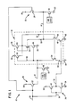
- FIG. 1 shows a circuit diagram of a data transmission system 10 according to one form of the present invention.
- Data buses 12 and 14 have NMOS field effect transistors 16 and 18, respectively, attached thereto for transfer of data signals to these buses.
- Each transistor 16 and 18 is connected to a power supply terminal 30 (shown as ground) and has some Bus Logic associated therewith which determines when a signal will be placed on the bus.
- the term "data” as used herein refers to any type of digital signal, and it specifically encompasses control, address, and data signals.
- each bus 12 and 14 will normally have a receiver circuit (not shown) attached thereto for receiving the signals appearing on the buses.
- Supply means 20 shown as NMOS field effect transistors 22 and 24 in the Figure 1 embodiment, are connected between a power supply terminal 26 and buses 12 and 14, respectively.
- the gate of each transistor 22 and 24 is connected to control line 28 which receives a digital control signal (such as a clock signal) from a device (not shown).
- Transistors 22 and 24 respond to a "high" value of the control signal by switching on thereby connecting power supply terminal 26 to buses 12 and 14.
- data buses 12 and 14 are precharged to essentially the voltage level of power supply terminals 26.
- Power supply terminals 26 and 30 are at potentials which represent the two logic levels appearing on data buses 12 and 14. Either one can be high relative to the other. However, in the preferred embodiment shown in Figure 1, power supply 26 is high relative to power supply 30.
- Data buses 12 and 14 are thereby precharged to a logical high level. Precharging to such a high level is advantageous because the time required for transistor 16 or 18 to "pull" the bus line low is generally faster than the time it would take to
- Data transmission system 10 also includes circuit means 32 connecting buses 12 and 14.
- circuit means 32 responds to a data signal on bus 12 or 14 at the voltage level provided by power supply terminal 30 and transfers the signal to the other bus.
- Circuit means 32 also responds to a "low” value of the control signal on control line 28. In this manner, when a "high" control signal appears on line 28 allowing supply means 20 to precharge data buses 12 and 14, circuit means 32 is in an "inactive" state.
- circuit means 32 is placed in an “active” state and can detect and transmit to the other bus any new voltage level placed on one of the buses by NMOS transistors 16 or 18.
- supply means 20 and circuit means 32 can be configured so that buses 12 and 14 are precharged on a "low” control signal and circuit means 32 is active on a "high” control signal.
- Data transmission system 10 further includes an inverter 34 having an input line 36 connected to control line 28 and an output line 38 connected to circuit means 32.
- Inverter 34 receives the control signal at input line 36 and provides a complementary control signal at output line 38.
- inverter 34 is a CMOS type inverter which includes PMOS field effect transistor 40 and NMOS field effect transistor 42 connected in series between power supply terminals 26 and 30.
- Output line 38 of inverter 34 is connected to the gates of NMOS field effect transistors 44 and 46.
- Transistors 44 and 46 connect circuit means 32 to power supply terminals 30.
- Circuit means 32 includes a NAND gate having input lines 48 and 50 and an output line 52.
- Input line 48 is connected to data bus 12 and input line 50 is connected to data bus 14.
- Output line 52 is connected to the gates of NMOS field effect transistors 54 and 56.
- Transistor 54 is connected between data bus 12 and transistor 44, while transistor 56 is connected between data bus 14 and transistor 46.
- the NAND gate also has PMOS field effect transistors 58 and 60 and NMOS field effect transistors 62 and 64.
- Transistor 58 is connected between power supply terminal 26 and the NAND gate output line 52 with its gate connected to data bus 12.
- Transistor 60 is connected between power supply terminal 26 and the NAND gate output line 52 with its gate connected to data bus 14.
- Transistors 62 and 64 are series connected between the NAND gate output line 52 and power supply terminal 30.
- the gate of transistor 62 is connected to data bus 14 and the gate of transistor 64 is connected to data bus 12.
- data transmission system 10 receives a "high" control signal on control line 28 which will switch on transistors 22 and 24 allowing data buses 12 and 14 to be precharged through power supply terminals 26.
- the "high" control signal on line 28 will be inverted to a "low” value by inverter 34. This low” value will be less than the threshold voltage of transistor 44 or 46 thereby keeping circuit means 32 inactive.
- FIG. 2 shows another embodiment of the present invention with like numbers representing similar elements to those described with reference to Figure 1.
- the circuit means 32 comprises inverters 66 and 68, transfer gates 70 and 72, and NMOS field effect transistors 74, 76, 78 and 80.
- Inverter 66 is a CMOS type inverter with PMOS field effect transistor 82 and NMOS field effect transistor 84 series connected between power supply terminals 26 and 30. Inverter 66 has an input 86 connected to data bus 12 and an output 88 connected to the input 90 of transfer gate 70.
- Transfer gate 70 is a PN channel combination gate having an NMOS field effect transistor 92 connected in parallel to a PMOS field effect transistor 94.
- the gate of transistor 92 is connected to the output line 38 of inverter 34 and receives a complementary control signal therefrom.
- the gate of transistor 94 is connected to control line 28 and receives a control signal therefrom.
- Transistor 74 is connected between data bus 14 and power supply terminal 30 with its gate connected to the output 96 of transfer gate 70.
- Transistor 80 is connected between output 96 of transfer gate 70 and power supply terminal 30.
- Inverter 68 is a CMOS type inverter with PMOS field effect transistor 98 and NMOS field effect transistor 100 series connected between power supply terminals 26 and 30. Inverter 68 has an input 102 connected to data bus 14 and an output 104 connected to the input 106 of transfer gate 72.
- Transfer gate 72 is a PN channel combination gate having an NMOS field effect transistor 108 connected in parallel to a PMOS field effect transistor 110.
- the gate of transistor 108 is connected to the output line 38 of inverter 34 and receives a complementary control signal.
- the gate of transistor 110 is connected to control line 28 and receives a control signal.
- Transistor 76 is connected between data bus 12 and power supply terminal 30 with its gate connected to the output 112 of transfer gate 72.
- Transistor 78 is connected between output 112 of transfer gate 72 and power supply terminal 30.
- data transmission system 10 shown in Figure 2 will receive a "high" control signal on control line 28 which will switch on transistors 22 and 24 allowing data buses 12 and 14 to be precharged through power supply terminals 26.
- the "high" control signal on line 28 will be received by the gate of transistors 78 and 80. This will pull outputs 112 and 96 of transfer gates 72 and 70, respectively, to a low value which prevents transistors 76 and 74 from conducting.
- inverter 66 will provide a "high” at output 88. This "high” at output 88 passes through transfer gate 70 and turns on transistor 74 thereby connecting bus 14 to power supply terminal 30 which is “low”.
- inverter 68 will provide a "high” at output 104 which passes through transfer gate 72, turning on transistor 76, and connecting bus 12 to power supply terminal 30.
- Figure 3 shows another embodiment of the present invention with like numbers representing similar elements to those described with reference to Figures 1 and 2.
- the circuit means 32 comprises inverters 66 and 68, transfer gates 114 and 116, and NMOS field effect transistors 74, 76, 78 and 80.
- the Figure 3 embodiment has N channel transfer gates 114 and 116. More specifically, transfer gates 114 and 116 include NMOS field effect transistors 118 and 120, respectively. The gates of each transistor 118 and 120 are connected to output line 38 of inverter 34 and receive a complementary control signal therefrom.
- data transmission system 10 shown in Figure 3 will receive a "high" control signal on control line 28 which will switch on transistors 22 and 24 allowing data buses 12 and 14 to be precharged through power supply terminals 26.
- the "high" control signal on line 28 will be received by the gate of transistors 78 and 80. This will pull outputs 112 and 96 of transfer gates 116 and 114, respectively, to a low value which prevents transistors 76 and 74 from conducting.
- the "low" signal (complementary control signal) on output line 38 of inverter 34 will be received by the gates of NMOS transistors 120 and 118 preventing transfer gates 116 and 118 from conducting.
- circuit means 32 will remain inactive as long as the control signal on line 28 is "high".
- Figure 4 shows another embodiment of the present invention with like numbers representing similar elements to those described with reference to Figures 1, 2 and 3.
- the circuit means 32 comprises inverters 66 and 68, transfer gates 122 and 124, and NMOS field effect transistors 74, 76, 78 and 80.
- the Figure 4 embodiment has P channel transfer gates 122 and 124. More specifically, transfer gates 122 and 124 include PMOS field effect transistors 126 and 128, respectively. The gates of each transistor 126 and 128 is connected to control line 28 and receives a control signal therefrom.
- the Figure 4 embodiment has no inverter 34.
- data transmission system 10 shown in Figure 4 will receive a "high" control signal on control line 28 which will switch on transistors 22 and 24 allowing data buses 12 and 14 to be precharged through power supply terminals 26.
- the "high" control signal on line 28 will be received by the gate of transistors 78 and 80. This will pull outputs 112 and 96 of transfer gates 124 and 122, respectively, to a low value which prevents transistors 76 and 74 from conducting.
- the "high" signal on line 28 will be received by the gates of PMOS transistors 128 and 126 preventing transfer gates 124 and 126 from conducting.
- circuit means 32 will remain inactive as long as the control signal on line 28 is "high".
- each of the buses is precharged to a first voltage level which in a preferred form is "high".
- first voltage level which in a preferred form is "low”.
- pull up transistors would be attached to the buses and be responsive to the Bus Logic for placing a data signal at a second voltage level on the bus.
Landscapes
- Engineering & Computer Science (AREA)
- General Engineering & Computer Science (AREA)
- Theoretical Computer Science (AREA)
- Computer Hardware Design (AREA)
- Physics & Mathematics (AREA)
- General Physics & Mathematics (AREA)
- Logic Circuits (AREA)
- Dram (AREA)
- Small-Scale Networks (AREA)
- Bus Control (AREA)
- Dc Digital Transmission (AREA)
Applications Claiming Priority (2)
| Application Number | Priority Date | Filing Date | Title |
|---|---|---|---|
| US07224023 US4918329B1 (en) | 1988-07-25 | 1988-07-25 | Data transmission system |
| US224023 | 1988-07-25 |
Publications (2)
| Publication Number | Publication Date |
|---|---|
| EP0352965A2 true EP0352965A2 (de) | 1990-01-31 |
| EP0352965A3 EP0352965A3 (de) | 1990-08-29 |
Family
ID=22838977
Family Applications (1)
| Application Number | Title | Priority Date | Filing Date |
|---|---|---|---|
| EP89307364A Withdrawn EP0352965A3 (de) | 1988-07-25 | 1989-07-20 | Datenübertragungssystem |
Country Status (4)
| Country | Link |
|---|---|
| US (1) | US4918329B1 (de) |
| EP (1) | EP0352965A3 (de) |
| JP (1) | JPH0260341A (de) |
| CA (1) | CA1304805C (de) |
Cited By (1)
| Publication number | Priority date | Publication date | Assignee | Title |
|---|---|---|---|---|
| EP0468583B1 (de) * | 1990-07-27 | 2001-06-20 | Koninklijke Philips Electronics N.V. | Treiberschaltkreis |
Families Citing this family (7)
| Publication number | Priority date | Publication date | Assignee | Title |
|---|---|---|---|---|
| JP2561167B2 (ja) * | 1989-04-18 | 1996-12-04 | 三菱電機株式会社 | バス回路 |
| US5239661A (en) * | 1989-08-18 | 1993-08-24 | Mitsubishi Denki Kabushiki Kaisha | Hierarchical bus circuit having decoder generating local buses and devices select signals enabling switching elements to perform data transfer operations |
| JPH0377129A (ja) * | 1989-08-18 | 1991-04-02 | Mitsubishi Electric Corp | プリチャージ方式バス回路 |
| US5030857A (en) * | 1989-08-25 | 1991-07-09 | Ncr Corporation | High speed digital computer data transfer system having reduced bus state transition time |
| US5019720A (en) * | 1990-03-12 | 1991-05-28 | Ncr Corporation | Integrated circuit driver for serial bus having output overvoltage protection |
| US5511171A (en) * | 1993-02-26 | 1996-04-23 | 3Com Corporation | Apparatus for live bus insertion of add-on devices |
| JP3625881B2 (ja) * | 1994-12-20 | 2005-03-02 | 株式会社ルネサステクノロジ | バスシステム及びバスセンスアンプ |
Family Cites Families (14)
| Publication number | Priority date | Publication date | Assignee | Title |
|---|---|---|---|---|
| US3938094A (en) * | 1971-08-31 | 1976-02-10 | Texas Instruments Incorporated | Computing system bus |
| US4154978A (en) * | 1977-12-08 | 1979-05-15 | Operating Systems, Inc. | Self-contained bidirectional amplifying repeater |
| US4516199A (en) * | 1979-10-11 | 1985-05-07 | Nanodata Computer Corporation | Data processing system |
| US4527237A (en) * | 1979-10-11 | 1985-07-02 | Nanodata Computer Corporation | Data processing system |
| US4404474A (en) * | 1981-02-06 | 1983-09-13 | Rca Corporation | Active load pulse generating circuit |
| JPS5833739A (ja) * | 1981-08-21 | 1983-02-28 | Toshiba Corp | バスライン駆動回路 |
| DE3133579A1 (de) * | 1981-08-25 | 1983-03-24 | Siemens AG, 1000 Berlin und 8000 München | Bus-steuer-einheit fuer ein vlsi-rechenwerk und verfahren zu ihrem betrieb |
| US4500988A (en) * | 1982-03-08 | 1985-02-19 | Sperry Corporation | VLSI Wired-OR driver/receiver circuit |
| US4488066A (en) * | 1982-11-08 | 1984-12-11 | At&T Bell Laboratories | Databus coupling arrangement using transistors of complementary conductivity type |
| DE3319980A1 (de) * | 1983-06-01 | 1984-12-06 | Siemens AG, 1000 Berlin und 8000 München | Integrierbares busorientiertes uebertragungssystem |
| JPS6051323A (ja) * | 1983-08-31 | 1985-03-22 | Toshiba Corp | Cmos伝送回路 |
| JPS6055458A (ja) * | 1983-09-05 | 1985-03-30 | Matsushita Electric Ind Co Ltd | Cmosトランジスタ回路 |
| US4621202A (en) * | 1984-11-13 | 1986-11-04 | Motorola, Inc. | Bi-directional bus isolation circuit |
| US4656626A (en) * | 1984-12-14 | 1987-04-07 | Itt Corporation | Apparatus and method for providing dynamically assigned switch paths |
-
1988
- 1988-07-25 US US07224023 patent/US4918329B1/en not_active Expired - Lifetime
-
1989
- 1989-06-02 CA CA000601609A patent/CA1304805C/en not_active Expired - Lifetime
- 1989-06-28 JP JP1164117A patent/JPH0260341A/ja active Pending
- 1989-07-20 EP EP89307364A patent/EP0352965A3/de not_active Withdrawn
Cited By (1)
| Publication number | Priority date | Publication date | Assignee | Title |
|---|---|---|---|---|
| EP0468583B1 (de) * | 1990-07-27 | 2001-06-20 | Koninklijke Philips Electronics N.V. | Treiberschaltkreis |
Also Published As
| Publication number | Publication date |
|---|---|
| US4918329A (en) | 1990-04-17 |
| US4918329B1 (en) | 1993-06-01 |
| CA1304805C (en) | 1992-07-07 |
| EP0352965A3 (de) | 1990-08-29 |
| JPH0260341A (ja) | 1990-02-28 |
Similar Documents
| Publication | Publication Date | Title |
|---|---|---|
| EP0047128B1 (de) | Eine Ausgangspufferschaltung | |
| US4806786A (en) | Edge set/reset latch circuit having low device count | |
| KR0136233B1 (ko) | 인터페이스 회로 | |
| EP0191074B1 (de) | Hilfskreis zur verbesserung der anstiegszeit eines elektronischen signals | |
| US4500988A (en) | VLSI Wired-OR driver/receiver circuit | |
| JPH06169252A (ja) | プログラム可能な論理回路装置 | |
| JPH0142013B2 (de) | ||
| US4686396A (en) | Minimum delay high speed bus driver | |
| GB2289808A (en) | CMOS driver with programmable switching speed | |
| US4918329A (en) | Data transmission system | |
| US6300795B1 (en) | Multiple-bit, current mode data bus | |
| EP0235889B1 (de) | Datenleseschaltung für eine Halbleiter-Speichervorrichtung | |
| EP0468583B1 (de) | Treiberschaltkreis | |
| US5034634A (en) | Multiple level programmable logic integrated circuit | |
| KR940003448A (ko) | 반도체 기억장치 | |
| US4654826A (en) | Single device transfer static latch | |
| JPH0763138B2 (ja) | 論理デ−タ伝送バスの予負荷回路 | |
| US6704826B1 (en) | Digital signal isolation | |
| US6236234B1 (en) | High-speed low-power consumption interface circuit | |
| US5200653A (en) | Tristate output gate structure particularly for cmos integrated circuits | |
| US6150844A (en) | High voltage tolerance output stage | |
| US5880606A (en) | Programmable driver circuit for multi-source buses | |
| US6624661B2 (en) | Programmable drive circuit for I/O port | |
| JP2937349B2 (ja) | 半導体集積回路 | |
| EP1094396A2 (de) | Bussystem zur Erhöhung der Übertragungsgeschwindigkeit |
Legal Events
| Date | Code | Title | Description |
|---|---|---|---|
| PUAI | Public reference made under article 153(3) epc to a published international application that has entered the european phase |
Free format text: ORIGINAL CODE: 0009012 |
|
| AK | Designated contracting states |
Kind code of ref document: A2 Designated state(s): DE FR GB |
|
| PUAL | Search report despatched |
Free format text: ORIGINAL CODE: 0009013 |
|
| AK | Designated contracting states |
Kind code of ref document: A3 Designated state(s): DE FR GB |
|
| 17P | Request for examination filed |
Effective date: 19901215 |
|
| 17Q | First examination report despatched |
Effective date: 19930622 |
|
| RAP1 | Party data changed (applicant data changed or rights of an application transferred) |
Owner name: NCR INTERNATIONAL INC. |
|
| STAA | Information on the status of an ep patent application or granted ep patent |
Free format text: STATUS: THE APPLICATION IS DEEMED TO BE WITHDRAWN |
|
| 18D | Application deemed to be withdrawn |
Effective date: 19940104 |