EP0350833A2 - Integrated circuit package structure - Google Patents
Integrated circuit package structure Download PDFInfo
- Publication number
- EP0350833A2 EP0350833A2 EP89112574A EP89112574A EP0350833A2 EP 0350833 A2 EP0350833 A2 EP 0350833A2 EP 89112574 A EP89112574 A EP 89112574A EP 89112574 A EP89112574 A EP 89112574A EP 0350833 A2 EP0350833 A2 EP 0350833A2
- Authority
- EP
- European Patent Office
- Prior art keywords
- integrated circuit
- base member
- support plate
- circuit substrate
- mold
- Prior art date
- Legal status (The legal status is an assumption and is not a legal conclusion. Google has not performed a legal analysis and makes no representation as to the accuracy of the status listed.)
- Granted
Links
Images


Classifications
-
- H—ELECTRICITY
- H05—ELECTRIC TECHNIQUES NOT OTHERWISE PROVIDED FOR
- H05K—PRINTED CIRCUITS; CASINGS OR CONSTRUCTIONAL DETAILS OF ELECTRIC APPARATUS; MANUFACTURE OF ASSEMBLAGES OF ELECTRICAL COMPONENTS
- H05K3/00—Apparatus or processes for manufacturing printed circuits
- H05K3/22—Secondary treatment of printed circuits
- H05K3/28—Applying non-metallic protective coatings
- H05K3/284—Applying non-metallic protective coatings for encapsulating mounted components
-
- H—ELECTRICITY
- H01—ELECTRIC ELEMENTS
- H01L—SEMICONDUCTOR DEVICES NOT COVERED BY CLASS H10
- H01L23/00—Details of semiconductor or other solid state devices
- H01L23/28—Encapsulations, e.g. encapsulating layers, coatings, e.g. for protection
- H01L23/31—Encapsulations, e.g. encapsulating layers, coatings, e.g. for protection characterised by the arrangement or shape
- H01L23/3107—Encapsulations, e.g. encapsulating layers, coatings, e.g. for protection characterised by the arrangement or shape the device being completely enclosed
-
- H—ELECTRICITY
- H01—ELECTRIC ELEMENTS
- H01L—SEMICONDUCTOR DEVICES NOT COVERED BY CLASS H10
- H01L23/00—Details of semiconductor or other solid state devices
- H01L23/48—Arrangements for conducting electric current to or from the solid state body in operation, e.g. leads, terminal arrangements ; Selection of materials therefor
- H01L23/488—Arrangements for conducting electric current to or from the solid state body in operation, e.g. leads, terminal arrangements ; Selection of materials therefor consisting of soldered or bonded constructions
- H01L23/495—Lead-frames or other flat leads
- H01L23/49503—Lead-frames or other flat leads characterised by the die pad
-
- H—ELECTRICITY
- H01—ELECTRIC ELEMENTS
- H01L—SEMICONDUCTOR DEVICES NOT COVERED BY CLASS H10
- H01L23/00—Details of semiconductor or other solid state devices
- H01L23/48—Arrangements for conducting electric current to or from the solid state body in operation, e.g. leads, terminal arrangements ; Selection of materials therefor
- H01L23/488—Arrangements for conducting electric current to or from the solid state body in operation, e.g. leads, terminal arrangements ; Selection of materials therefor consisting of soldered or bonded constructions
- H01L23/495—Lead-frames or other flat leads
- H01L23/49517—Additional leads
- H01L23/49531—Additional leads the additional leads being a wiring board
-
- H—ELECTRICITY
- H01—ELECTRIC ELEMENTS
- H01L—SEMICONDUCTOR DEVICES NOT COVERED BY CLASS H10
- H01L23/00—Details of semiconductor or other solid state devices
- H01L23/48—Arrangements for conducting electric current to or from the solid state body in operation, e.g. leads, terminal arrangements ; Selection of materials therefor
- H01L23/488—Arrangements for conducting electric current to or from the solid state body in operation, e.g. leads, terminal arrangements ; Selection of materials therefor consisting of soldered or bonded constructions
- H01L23/495—Lead-frames or other flat leads
- H01L23/49541—Geometry of the lead-frame
- H01L23/49548—Cross section geometry
- H01L23/49551—Cross section geometry characterised by bent parts
-
- H—ELECTRICITY
- H01—ELECTRIC ELEMENTS
- H01L—SEMICONDUCTOR DEVICES NOT COVERED BY CLASS H10
- H01L23/00—Details of semiconductor or other solid state devices
- H01L23/48—Arrangements for conducting electric current to or from the solid state body in operation, e.g. leads, terminal arrangements ; Selection of materials therefor
- H01L23/488—Arrangements for conducting electric current to or from the solid state body in operation, e.g. leads, terminal arrangements ; Selection of materials therefor consisting of soldered or bonded constructions
- H01L23/498—Leads, i.e. metallisations or lead-frames on insulating substrates, e.g. chip carriers
- H01L23/49811—Additional leads joined to the metallisation on the insulating substrate, e.g. pins, bumps, wires, flat leads
-
- H—ELECTRICITY
- H01—ELECTRIC ELEMENTS
- H01L—SEMICONDUCTOR DEVICES NOT COVERED BY CLASS H10
- H01L2224/00—Indexing scheme for arrangements for connecting or disconnecting semiconductor or solid-state bodies and methods related thereto as covered by H01L24/00
- H01L2224/01—Means for bonding being attached to, or being formed on, the surface to be connected, e.g. chip-to-package, die-attach, "first-level" interconnects; Manufacturing methods related thereto
- H01L2224/42—Wire connectors; Manufacturing methods related thereto
- H01L2224/47—Structure, shape, material or disposition of the wire connectors after the connecting process
- H01L2224/48—Structure, shape, material or disposition of the wire connectors after the connecting process of an individual wire connector
- H01L2224/4805—Shape
- H01L2224/4809—Loop shape
- H01L2224/48091—Arched
-
- H—ELECTRICITY
- H01—ELECTRIC ELEMENTS
- H01L—SEMICONDUCTOR DEVICES NOT COVERED BY CLASS H10
- H01L2224/00—Indexing scheme for arrangements for connecting or disconnecting semiconductor or solid-state bodies and methods related thereto as covered by H01L24/00
- H01L2224/01—Means for bonding being attached to, or being formed on, the surface to be connected, e.g. chip-to-package, die-attach, "first-level" interconnects; Manufacturing methods related thereto
- H01L2224/42—Wire connectors; Manufacturing methods related thereto
- H01L2224/47—Structure, shape, material or disposition of the wire connectors after the connecting process
- H01L2224/48—Structure, shape, material or disposition of the wire connectors after the connecting process of an individual wire connector
- H01L2224/481—Disposition
- H01L2224/48151—Connecting between a semiconductor or solid-state body and an item not being a semiconductor or solid-state body, e.g. chip-to-substrate, chip-to-passive
- H01L2224/48221—Connecting between a semiconductor or solid-state body and an item not being a semiconductor or solid-state body, e.g. chip-to-substrate, chip-to-passive the body and the item being stacked
- H01L2224/48245—Connecting between a semiconductor or solid-state body and an item not being a semiconductor or solid-state body, e.g. chip-to-substrate, chip-to-passive the body and the item being stacked the item being metallic
- H01L2224/48247—Connecting between a semiconductor or solid-state body and an item not being a semiconductor or solid-state body, e.g. chip-to-substrate, chip-to-passive the body and the item being stacked the item being metallic connecting the wire to a bond pad of the item
-
- H—ELECTRICITY
- H01—ELECTRIC ELEMENTS
- H01L—SEMICONDUCTOR DEVICES NOT COVERED BY CLASS H10
- H01L24/00—Arrangements for connecting or disconnecting semiconductor or solid-state bodies; Methods or apparatus related thereto
- H01L24/01—Means for bonding being attached to, or being formed on, the surface to be connected, e.g. chip-to-package, die-attach, "first-level" interconnects; Manufacturing methods related thereto
- H01L24/42—Wire connectors; Manufacturing methods related thereto
- H01L24/47—Structure, shape, material or disposition of the wire connectors after the connecting process
- H01L24/48—Structure, shape, material or disposition of the wire connectors after the connecting process of an individual wire connector
-
- H—ELECTRICITY
- H01—ELECTRIC ELEMENTS
- H01L—SEMICONDUCTOR DEVICES NOT COVERED BY CLASS H10
- H01L2924/00—Indexing scheme for arrangements or methods for connecting or disconnecting semiconductor or solid-state bodies as covered by H01L24/00
- H01L2924/0001—Technical content checked by a classifier
- H01L2924/00014—Technical content checked by a classifier the subject-matter covered by the group, the symbol of which is combined with the symbol of this group, being disclosed without further technical details
-
- H—ELECTRICITY
- H01—ELECTRIC ELEMENTS
- H01L—SEMICONDUCTOR DEVICES NOT COVERED BY CLASS H10
- H01L2924/00—Indexing scheme for arrangements or methods for connecting or disconnecting semiconductor or solid-state bodies as covered by H01L24/00
- H01L2924/01—Chemical elements
- H01L2924/01014—Silicon [Si]
-
- H—ELECTRICITY
- H01—ELECTRIC ELEMENTS
- H01L—SEMICONDUCTOR DEVICES NOT COVERED BY CLASS H10
- H01L2924/00—Indexing scheme for arrangements or methods for connecting or disconnecting semiconductor or solid-state bodies as covered by H01L24/00
- H01L2924/01—Chemical elements
- H01L2924/01039—Yttrium [Y]
-
- H—ELECTRICITY
- H01—ELECTRIC ELEMENTS
- H01L—SEMICONDUCTOR DEVICES NOT COVERED BY CLASS H10
- H01L2924/00—Indexing scheme for arrangements or methods for connecting or disconnecting semiconductor or solid-state bodies as covered by H01L24/00
- H01L2924/095—Indexing scheme for arrangements or methods for connecting or disconnecting semiconductor or solid-state bodies as covered by H01L24/00 with a principal constituent of the material being a combination of two or more materials provided in the groups H01L2924/013 - H01L2924/0715
- H01L2924/097—Glass-ceramics, e.g. devitrified glass
- H01L2924/09701—Low temperature co-fired ceramic [LTCC]
-
- H—ELECTRICITY
- H01—ELECTRIC ELEMENTS
- H01L—SEMICONDUCTOR DEVICES NOT COVERED BY CLASS H10
- H01L2924/00—Indexing scheme for arrangements or methods for connecting or disconnecting semiconductor or solid-state bodies as covered by H01L24/00
- H01L2924/10—Details of semiconductor or other solid state devices to be connected
- H01L2924/11—Device type
- H01L2924/14—Integrated circuits
-
- H—ELECTRICITY
- H01—ELECTRIC ELEMENTS
- H01L—SEMICONDUCTOR DEVICES NOT COVERED BY CLASS H10
- H01L2924/00—Indexing scheme for arrangements or methods for connecting or disconnecting semiconductor or solid-state bodies as covered by H01L24/00
- H01L2924/15—Details of package parts other than the semiconductor or other solid state devices to be connected
- H01L2924/181—Encapsulation
-
- H—ELECTRICITY
- H01—ELECTRIC ELEMENTS
- H01L—SEMICONDUCTOR DEVICES NOT COVERED BY CLASS H10
- H01L2924/00—Indexing scheme for arrangements or methods for connecting or disconnecting semiconductor or solid-state bodies as covered by H01L24/00
- H01L2924/19—Details of hybrid assemblies other than the semiconductor or other solid state devices to be connected
- H01L2924/1901—Structure
- H01L2924/1904—Component type
- H01L2924/19041—Component type being a capacitor
-
- H—ELECTRICITY
- H01—ELECTRIC ELEMENTS
- H01L—SEMICONDUCTOR DEVICES NOT COVERED BY CLASS H10
- H01L2924/00—Indexing scheme for arrangements or methods for connecting or disconnecting semiconductor or solid-state bodies as covered by H01L24/00
- H01L2924/19—Details of hybrid assemblies other than the semiconductor or other solid state devices to be connected
- H01L2924/191—Disposition
- H01L2924/19101—Disposition of discrete passive components
- H01L2924/19107—Disposition of discrete passive components off-chip wires
-
- H—ELECTRICITY
- H01—ELECTRIC ELEMENTS
- H01L—SEMICONDUCTOR DEVICES NOT COVERED BY CLASS H10
- H01L2924/00—Indexing scheme for arrangements or methods for connecting or disconnecting semiconductor or solid-state bodies as covered by H01L24/00
- H01L2924/30—Technical effects
- H01L2924/35—Mechanical effects
- H01L2924/351—Thermal stress
- H01L2924/3511—Warping
Definitions
- the present invention relates to integrated circuits and more particularly to package structures for integrated circuits, including hybrid integrated circuits in which active and passive elements are incorporated.
- epoxy resin is very popular and widely used as a molding material, and an insert-mold method is utilised which lends itself to mass production.
- a circuit substrate and a lead frame are incorporated in molding material during the mold process.
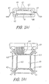
- Figs. 1(a) and 1(b) show respectively a schematic cross-sectional view of a conventional hybrid integrated circuit and a plan view of a lead frame used therein.
- the lead frame 60 has a square support plate 61 centrally arranged, which plate is sometimes called a stage or tab. On the support plate 61 a circuit substrate 62 is mounted and is selectively connected to leads 63 by a wire bonding method. The above structure is finally molded as a package 64 of epoxy resin material.
- the circuit substrate 62 comprises a base member 66, for example of alumina ceramic, epoxy glass or silicon, and active and passive elements 67 disposed on the base member 66.
- the expansion coefficient of the base member 66 is smaller than that of the molding material, and adhesive strength between the mold material and the support plate 61 (e.g. a metal plate) is less than that between the mold material and the base member 66.
- the device hybrid integrated circuits or integrated circuits are sometimes called devices, for brevity, in the present application
- the lower portion of the mold package 64 may not withstand the stress induced, which is concentrated along a periphery of the support plate 61, and finally the mold package 64 of the device may manifest a crack 65 along a side or along two neighbouring sides of the square periphery of the support plate, as shown in Fig. 1(a).
- the device comprises a lead frame, a support plate thereof having a plurality of cuts extending from its periphery towards the centre of the support plate.
- the two disclosures mentioned above are concerned each with a semiconductor integrated circuit which comprises a single monolithic semiconductor chip mounted on the support plate.
- the semiconductor chip size (surface area) is comparatively small compared with the outline dimensions of the mold package.
- An embodiment of the present invention can provide a hybrid integrated circuit which is more resistant to the effects of repeated heat cycles of expansion and contraction.
- An embodiment of the present invention can provide a package structure of a hybrid integrated circuit, which affords excellent durability even when hybrid integrated circuit is constructed with a notably large scale of integration.
- An embodiment of the present invention can provide a hybrid integrated circuit which can be fabricated by methods similar to those conventionally used.
- An embodiment of the invention can provide a package structure of a hybrid integrated circuit such that reduced or minimum deformation of the mold package occurs between premolding and postmolding states.
- Embodiments of the present invention can provide hybrid integrated circuits which are more resistant to the effects of repeated cycles of thermal expansion and contraction.
- a hybrid integrated circuit in accordance with an embodiment of the present invention comprises:- a circuit substrate which includes a base member and at least one of a semiconductor active element and a passive element disposed on the base member; a lead frame comprising at least a plurality of leads and a support plate arranged in outer and inner portions thereof, each lead having an inner lead and an outer lead; the circuit substrate disposed on the support plate and selectively connected with inner ends of the inner leads; and a mold of resin material packaging the circuit substrate, support plate and inner leads; and the support plate having an opening for exposing the bottom surface of the circuit substrate to the mold, and the ratio of the exposed bottom surface to an entire bottom surface thereof being greater than 50%.
- the above device structure is of special merit when the circuit substrate has a large size such that the ratio of surface area of the circuit substrate to principal surface area of the mold package becomes greater than 60%.
- the molding material of epoxy resin contacts the bottom surface of the circuit substrate with a stronger adhesive force than in a case in which mold material contacts the support plate directly, as in the prior art mentioned above. Further, because the support plate area is reduced as compared with the case in which no opening is provided, stress due to thermal expansion of the support plate is also reduced and is further distributed over the entire surface thereof. These factors combine in effect to provide for the avoidance of or the reduction of rate of occurrence of package crack defects.
- the relationship between mold thickness above and below the circuit substrate is selectively chosen, in dependence upon the relationship between expansion coefficients of the circuit substrate and the support plate.
- a preassembled hybrid for example, integrated circuit is heated up to about 175 o C which causes a deformation thereof.
- the deformation remains after the molding process, which is the cause of the characteristic change.
- the deformation can be reduced or eliminated with a package structure in accordance with an embodiment of the present invention.
- an integrated circuit for example a hybrid integrated circuit, comprising:- a circuit substrate, comprising a base member and at least one semiconductor element, an active element or a passive element, disposed on the base member, a lead frame comprising at least a plurality of leads and a support plate, respectively provided at outward and inward portions of the lead frame, and each lead having an inner lead portion and an outer lead portion, the circuit substrate being disposed on the support plate and selectively connected with inner ends of inner lead portions, a mold of resin material packaging the circuit substrate, support plate and inner lead portions, wherein the ratio of a mold thickness above the base member to that below the base member is substantially proportional to the ratio of the expansion of the base member to that of the support plate.
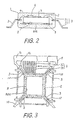
- FIG. 2 A hybrid integrated circuit in accordance with one embodiment (first embodiment) of the present invention is shown in cross-section in Fig. 2, and Fig. 3 is a top view of a lead frame 9 used in the first embodiment.
- the lead frame 9 is made of any of copper alloy, iron nickel alloy, etc.
- a circuit substrate 2 comprises a base member 5 and chip parts (6, 7) mounted and fixed thereon.
- the base member 5 is of insulating material such as alumina ceramic, epoxy glass, glass coated metal, oxide covered silicon, sapphire, etc.
- the chip parts may include any active and/or passive elements, such as a semiconductor active element 6 forming an integrated circuit, a capacitor chip 7, etc. These chip parts are bonded on the base member 5 by conductive bonding resin and terminals thereof are selectively connected to bonding pads on the base member 5 and/or are mutually interconnected.
- the circuit substrate 2 is mounted on a support plate 8 and is fixed thereon by heat resistive adhesive.
- a plurality of leads 3 of the lead frame 9 are arranged on each side of the circuit substrate 2, and a lead 3 is composed of an inner lead 31 and outer lead 32. An inside end of an inner lead 31 is connected selectively to a bonding pad on the base member 5.
- the whole structure, except for substantial portions of the leads 3, is molded in a mold package 4 of epoxy resin, forming a completed hybrid integrated circuit 1 in accordance with the first embodiment of the present invention.
- chip parts 6, 7 are mentioned as illustrations of possible active and passive elements.
- elements used in embodiments of the invention are not restricted to chip parts.
- they may be thick or thin film parts (not shown in Fig. 2), forming capacitors or resistors, which are directly formed on the base member 5 by screen printing or sputtering methods.
- the leads 3 and support plate 8 are integral parts of the lead frame 9, and the support plate 8 has an outline of a square shape having a square opening 80a therein. Therefore, the support plate 8 has four side strips forming a square outline, and is connected to the remainder of the lead frame by support bars 10.
- the opening 80a is formed with a predetermined size such that the remaining four side strips of the support plate 8 are of sufficient size to support the base member 5, it being preferable that the base member 5 does not extend beyond the outermost outline edges of the support plate. Dimensions of the base member 5 are indicated by broken lines 2 in Fig. 3.
- the support plate 8 is centrally located in the lead frame 9, and inside ends of inner leads 31 are disposed close to the support plate 8 for easy connection, by a wire bonding process, to bonding pads on the circuit substrate 2.
- An outside frame portion 11 and an interconnection bar 12 between leads 3 are removed after the molding process.
- the opening 80a functions to make or allow resin material flow freely to the bottom surface of the circuit substrate 2 (base member 5) and adhere thereto during a molding process of the mold package 4, utilising a transfer-mold method.
- Adhesive strengths against shearing force of bonds between epoxy resin of the mold package 4 and other parts such as base member 5 and support plate 8 comprised therein are shown in TABLE 1.
- the mold package 4, circuit substrate 2, support plate 8, etc. suffer different amounts of expansion.
- the mold material of package 4 directly contacts the base member 5 through the opening 80a (of predetermined size) and therefore, in this case (as seen from TABLE 1) the adhesive strength of the adhesion of the mold package 4 to the base member 5 is much greater than the adhesive strength achieved in a case in which a support plate without an opening is used, as in previous proposals.
- the lower portion of the package 4 under the base member 5 is fixed more rigidly thereto, and cannot easily move apart from the bottom surface of the base member 5.
- the effective area of the support plate 8 of the embodiment is remarkably reduced, stress due to expansion of the support plate is also reduced and further distributed to the overall fringe portions thereof, resulting in avoidance of stress concentration at the outer fringe portion only.
- the above two factors contribute to eliminate or reduce the chances of the package 4 cracking.
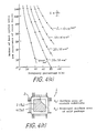
- Fig. 4(a) is a graph illustrating data indicating the relationships between percentage occupancy X of the circuit substrate 2 and tendency to crack occurrence for different package sizes (for support plates without openings). Percentage occupancy is indicated along the abscissa and is defined by the ratio of surface area S0 of the circuit substrate 2 (base member 5) to principal surface area S1 of the mold package. Tendency to crack occurrence is indicated along the ordinate and is defined by the number of heat cycles needed until a 10% rate of occurrence of crack defects is observed among test pieces. The percentage occupancy X is, therefore, expressed by a ratio S0/S1, S0 defining the surface area of circuit substrate 2 and S1 defining the principal surface area of mold package as shown in Fig. 4(b).
- circuit substrates having a square shape and a thickness of 0.5 mm but having different percentage occupancies were prepared in each of five groups having respective different mold package sizes. Further, a large number of lead frames, having different sizes of support plate of a square shape without an opening, were prepared corresponding to each of the five package size groups. The percentage occupancy becomes 80% when the surface areas of the support plate and circuit substrate are equal.
- each of the circuit substrates was mounted on the square support plate of a lead frame and fixed thereto by adhesive.
- Each test piece having a 4 mm thickness of the mold package 4 and as shown in Fig. 4(b), is obtained after molding in epoxy resin by a transfer-mold method.
- Different package outline dimensions were fabricated by changing the dimensions of the molding die. In this way, test pieces in five different package size groups were provided, each group including different percentage occupancies.
- Test piece were subjected to a heat cycle test which included the steps of dipping in a solution at -55 o C for five minutes and dipping in a solution at 125 o C for five minutes. The number of heat cycles needed to reach a state in which 10% of test pieces manifested a package crack was measured for each package size and occupancy percentage. The results are shown in Fig. 4(a).
- X denotes the ratio of surface area S0 of the circuit substrate to principal surface area S1 of the package. It can be seen from the Figure that, when either the package size becomes larger or the percentage occupancy X becomes larger, the package is more liable to be cracked. Liability to cracking is more seriously pronounced as package size grows larger. When X is larger than 60%, a package of the smallest size, 10 x 10 mm2, cannot withstand 1000 heat cycles, which is the criteria used for judging whether or not a package can be employed in practice.
- a semiconductor integrated circuit including a single semiconductor chip has at most a surface area of about 15 x 15 mm2, and the occupancy percentage X (ratio of area of the semiconductor chip to the package outline) is less than 50%, mostly less than 30%. Under these conditions the semiconductor chip is completely covered by epoxy resin and buried in the package, and there is very little chance of a package crack occurring. Therefore, package cracking has almost been left out of consideration.
- the occupancy percentage X is increased over 60%, the thickness of the package becomes comparatively small and the mold package becomes very susceptible to cracks.
- the package size is further increased above 20 x 20 mm2, resistance to cracking is further decreased, and finally it becomes almost impossible to obtain usable devices by using the square support plate without opening.
- a hybrid integrated circuit in accordance with an embodiment of the present invention enables the application of an occupancy percentage X of the circuit substrate in a range greater than 60% without significant package cracking, with the result that package size can be made smaller and integration density increased.
- a support plate having an opening is utilised.
- An example is explained for the first embodiment using Figs. 2 and 3.
- opening 80a allowing resin material to flow to the bottom surface of the circuit substrate 2 is formed in the support plate 8.
- Fig. 5 is a graph illustrating heat cycling test results when the tests were carried out on hybrid integrated circuits provided with openings 80a in their support plates. The circuits were subjected to alternate dipping steps into solutions at -55 o C and 125 o C for five minutes each.
- lead frames of copper alloy were employed, and the circuit substrates had a surface area of 28 x 28 mm2 and the percentage occupancy X thereof to the mold package was about 67%.
- the numerator of the above equation is preferably modified to a more precise expression such as "the exposed bottom area of the circuit substrate, directly contacting the mold package".
- the two definitions are the same or indicate almost the same area.
- the test results are illustrated in Fig. 5 and the curves therein indicate the probability of a mold package being cracked versus the number of heat cycles applied thereto. As the area ratio Y becomes larger, the curve moves toward the right and lower region in Fig. 5, which means the crack occurrence probability decreases. Each curve pertaining to a specific value of Y was obtained using 50 test pieces. The test results make clear that crack occurrence can be controlled by providing the opening 80a in the support plate 8.
- an opening of a square shape is formed in the support plate.
- the shape of the opening need not be restricted to a square shape.
- a rectangular shape may be used, for instance when the circuit substrate is rectangular. The shape may be changed depending on the design of the circuit substrate.
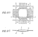
- Fig. 6(a) illustrates a second embodiment of the present invention.
- the Figure shows only a partial plan view of a lead frame omitting outer lead and frame portions thereof, because the omitted portions of the lead frame are substantially the same as those in Fig. 3.
- Four square stages 100 form the support plate, the stages being provided at respective corners of an assumed square shape having a side length 84.
- Each stage 100 is supported and connected to the remainder of the lead frame by a single support bar 10 extending in an outward diagonal direction.
- Chain lines 80e denote schematically the opening of the support plate 8, which is substantially the same as the exposed bottom surface area of the circuit substrate 2. Similar chain lines and similar reference numerals to 80e are used in following Figures.
- a stage 100 need not be restricted to square shape, but may be rectangular or circular in shape. Further, the number of stages may be increased depending on a size of the circuit substrate 2.
- Figs. 6(b) and 6(c) illustrate third and fourth embodiments of the present invention.
- connecting bars 101 have a width W1 less than that W0 of a stage 100.
- Figs. 6(d) and 6(e) illustrate fifth and sixth embodiments of the present invention, which are further modifications of the embodiment of Fig. 6(a).
- each stage 100 is supported by two support bars 10′ and 10 ⁇ .
- each stage 100 is supported by three support bars 10, 10′ and 10 ⁇ .
- mechanical strength is sometimes insufficient.
- the stage is easily subjected to deformation or a position shift, resulting in inferior quality in wire-bonding and in other respects.
- Figs. 6(d) or 6(e) increase the support strength of stages 100 by increasing the number of support bars to two or three.
- TABLE 2 shows measured displacements of a stage 100 after bonding a circuit substrate 2 thereon, for two different support bar structures as shown in Figs. 6(a) and 6(d) respectively.
- the displacements were measured in each of X-, Y- and Z-directions.
- Test pieces for these measurements had structures such that stages 100 were located substantially on each corner of a square 24 x 24 mm2, i.e. the side length 84 of Fig. 6(a) was about 24 mm, and a stage 100 formed a square of 3 x 3 mm2.
- the width of support bars 10, 10′ and 10 ⁇ of Fig. 6(d) was about 0.65 mm, and the length of support bars 10 of Fig.
- the base members forming the circuit substrates had a size of 23 x 23 mm2 and were made of alumina ceramic having a 0.5 mm thickness, and bonded on the stages by heat resistive silicon resin.
- TABLE 2 shows average data for 50 test pieces for both types, measured by a dial gauge and a microscope.
- the displacement decreases by a factor of about ten by changing the number of support bars from one to two.
- two support bars 10′ and 10 ⁇ are used for a stage, the directions thereof forming a right angle and being parallel to sides of the stage.
- further improvement can be expected for molding a larger size of circuit substrate.
- two support bars 10′ and 10 ⁇ form a right angle, each direction being parallel to a side of a square shape, and the remaining support bar 10 is arranged in an outward diagonal direction.
- Figs. 6(f) and 6(f′) illustrate a seventh embodiment of the present invention, in which Fig. 6(f) shows a partial plan view of a lead frame and Fig. 6(f′) shows a cross-section along the line A-A′ in Fig. 6(f).
- the plan view is very similar to that of Fig. 6(c), but, as shown in Fig. 6(f′), a stage 100 is displaced to a lower position from an original frame level.
- the inside ends of inner leads 31 are bent upwardly to an upper position in order to bring bonding positions of inner leads and the circuit substrate to the same level even when a thick circuit substrate is utilised.
- a connecting bar 101 has two further sloped portions and a horizontal portion, which contribute to relieve stress.
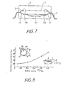
- Fig. 7 shows a schematic cross-section of a hybrid integrated circuit when a circuit substrate is mounted on this type of the lead frame (of Fig. 6(f)) having upwardly deformed inner leads and lowered stages and is molded in a package.
- FIGs. 6(g) and 6(g′) illustrate an eighth embodiment of the present invention, in which Fig. 6(g) is a plan view of the support plate and Fig. 6(g′) is a cross-sectional view thereof.
- a connecting bar 101 has an undulation in the same plane as the stages 100. The undulation makes the support plate more flexible and has an effect of relieving stress between the circuit substrate 2 and the support plate.
- Figs. 6(h) and 6(h′) illustrate a ninth embodiment of the present invention which is a modification of that of Fig. 6(d).
- the top or plan view of Fig. 6(h) is quite similar to that of Fig. 6(d).
- stages 100 are lowered and inner leads 31 are bent upwardly, with the result that the inside ends of the inner leads 31 are maintained at the same level as the surface of circuit substrate 2.
- Figs. 6(i) and 6(i′) illustrate a tenth embodiment of the present invention, which is a modification of the embodiments of Fig. 6(c) or Fig. 6(d).
- Stages 100 are mutually interconnected by connecting bars 101 and have each two support bars 10′ and 10 ⁇ .
- Stages 100 are lowered and the inside ends of inner leads 31 are bent upwardly as shown in Fig. 6(i′) which is similar in this respect to Figs. 6(f′) and 6(h′).
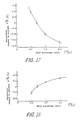
- Fig. 8 is a graph illustrating a relationship between a bending amount t and a width ratio W1, W0 between a connecting bar and a stage. These notations (t, W1, W0) are indicated in the illustrations inserted in Fig. 8.
- the shape of lead frame used for obtaining test data for the graph was of the type disclosed by Fig. 6(c).
- the reference character L denotes the side dimension of a square outline of the support plate, which was chosen to be a length of 24 mm.
- the dimension W0 was chosen to be 3 mm.
- the bending amount t was measured when the assembly of circuit substrate and lead frame was heated up to 175 o C, which is a package molding temperature.
- Fig. 8 shows that the smaller the width of connecting bar is, the less the bending amount is.
- Fig. 9 is a diagram illustrating a relationship between a bending amount t and the shape of connecting bar. Similar tests were performed at 175 o C using lead frames having support plate structures as shown in Fig. 6(c) and Figs. 6(f), 6(f′). The former group has a larger bending amount t than the latter group in which the support bar is (deliberately) bent and the stage is lowered.
- Fig. 10 is a graph illustrating probability of package cracking versus number of heat cycles. The tests for obtaining the graph data were performed using test pieces having an area ratio Y of about 60% and a side dimension L of 23 mm in Fig. 8.
- the curve indicated by encircled 2 illustrates crack probability data for the support plate structure of Fig. 6(c) where W1/W0 is 0.2;
- the curve indicated by encircled 3 shows data for Fig. 6(b);
- the curve indicated by encircled 4 shows data for Fig. 6(f) where W1/W0 is given as 0.2;
- the curve indicated by encircled 5 shows data for both the structure of Fig. 6(a) and the structure modified from Fig. 6(b) in which a connecting bar has an undulation.
- Fig. 10 shows that the crack occurrence probability (as against number of heat cycles) can be significantly reduced by providing the opening in the support plate, even when the hybrid integrated circuit has a high percentage occupancy (ratio of circuit substrate area to package size).
- integrated circuits for example hybrid integrated circuits, are required in which semiconductor active elements (and passive elements such as capacitors and resistors) are mounted on both surfaces of a base member 5 forming a circuit substrate 2.
- Fig. 11(a) is a schematic cross-sectional view of an example of such a (hybrid) device.
- Chip capacitors 7 are mounted on both sides of the base member 5 and a semiconductor chip 6 and a resistor 7′ are mounted on the upper surface thereof.
- the assembled circuit substrate 5 is bonded on a stage 100 of a support plate and is molded in a package 4.
- the lead frame used is of a type similar to that shown in Figs. 6(f) and 6(f′), but the inner leads 31 are not bent upwardly.
- Fig. 11(b) is a cross-sectional view of an embodiment of the present invention, having elements mounted on both surfaces of a base member, in this case a hybrid device.
- a lead frame such as is illustrated in Fig. 6(h) is used in this embodiment.
- two semiconductor integrated circuit chips 6 are mounted on a front surface of the circuit substrate 2, and passive chip elements 7 such as resistor, capacitor, etc., are soldered on both surfaces of the circuit substrate 2.
- integrated circuits e.g. hybrid circuits
- a lead frame having a support plate without an opening cannot be used.
- integrated circuits e.g. hybrid circuits
- a bonding method using adhesive is generally employed.
- another method can be used in which the circuit substrate 2 is clipped or pinched by or between a pair of clippers or pincer portions of the stage.
- Fig. 12 is a schematic cross-sectional view of a device in which tip portions of a stage 85 are separated into upper and lower portions 85a and 85b. Portions 85a and 85b clip or pinch a fringe or edge of a circuit substrate 2.
- x1 and x2 denote thicknesses of upper and lower portions of a mold package 4 with regard to the base member 5, which forms the circuit substrate 2 with chip parts (not shown).
- x2 represents a dimension (thickness) below the support plate 8, which is substantially equal to that below the base member 5.
- x1 and x2 are chosen to be almost equal, as shown in Fig.
- Figs. 14(a) and 14(b) States occurring during a transfer molding process are shown schematically and somewhat exaggeratedly in Figs. 14(a) and 14(b).
- Fig. 14(a) the assembled parts are inserted in a molding cavity 20 and heated up to about 175 o C, and the circuit substrate 2 and support plate 8 show a downward convex bend.
- the mold package is cooled down to room temperature. In this process, the shrinkage forces in the upper and lower portions of the mold package with regard to the circuit substrate 2 are almost equal; therefore, the resin mold hardens without recovery from the bent shape.
- FIG. 15(a) and 15(b) Another embodiment of the present invention utilises a package structure as illustrated in Figs. 15(a) and 15(b) to solve the above problem.
- Fig. 15(a) is a plan view of the embodiment, in which an upper portion of the mold material is partially removed, and Fig. 15(b) is a cross-sectional view thereof.
- the parts used therein are similar to those used in the previous embodiments.
- the device may be a hybrid or non-hybrid device, with elements mounted on one or both sides of a circuit substrate.
- a circuit substrate 2 has a square size of 23 x 23 mm2 and a 0.6 mm thickness.
- thick film resistors of 10 kilo-ohms were formed on both surfaces of a base member 5 by a printing method (instead of forming the circuit substrate 2 with chip parts).
- a film resistor is a sensitive passive element which can be used easily to detect deformation of the substrate on which the resistor is formed.
- Symbols x1 and x2 denote thickness of upper and lower portions of the mold package respectively.
- Several kinds of test pieces were fabricated to enable measurement of deformation, which depends on a relationship between x1 and x2, and the best conditions sought.
- the total thickness of x1 and x2 was changed over a range between 3 mm and 5 mm, and the ratio x1/x2 was changed over a range between 0.3 and 1.5.
- the device shapes in the molding process as shown in Figs. 16(a) and 16(b), which are illustrations of a kind similar to Figs. 14(a) and 14(b).
- Figs. 17 and 18 Test results for mold packages with film resistors are shown in the graphs of Figs. 17 and 18.
- the ordinates of the graphs in both Figures indicate resistance change in percent and the abscissae indicate the ratio x1/x2 of upper mold thickness to lower mold thickness.
- Fig. 17 shows data for resistors formed on the front surfaces of the base members 5 and
- Fig. 18 shows data for resistors formed on the bottom surfaces thereof.
- resistance value of a film resistor increases when the base member 5 on which the film resistor is formed is subjected to an upward convex deformation and, on the other hand, resistance value decreases when the substrate is subjected to an upward concave deformation.
- Test pieces were fabricated utilising alumina ceramic for the base member 5, having an expansion coefficient of about 7.2 x 10 ⁇ 6/ o C, and copper alloy for the support plate, having an expansion coefficient of about 6.9 x 10 ⁇ 6/ o C.
- the expansion of the former is much less than that of the latter, a little less than a half of the latter.
- the resistance change is almost null (zero) when x1/x2 is about 0.7.
- the thickness ratio x1/x2 is preferably selected to be in a range between 0.6 and 0.8.
- the expansion of the circuit substrate 2 is smaller than that of the support plate 8, and therefore the upper thickness x1 of the mold package above the base member 5 is selected to be smaller than the lower thickness x2 thereunder.
- the expansion of the base member 5 is larger than that of the support plate 8, for example when an iron-nickel alloy such as the so-called "41 alloy” is used therefor, the circuit substrate and the support plate show upward convex deformation when heated up. Therefore, the upper thickness x1 of the mold package above the circuit substrate is selected to be larger than the lower thickness x2 under the circuit substrate.
- test pieces had thick film resistors on the base member, being elements which are susceptible to deformation. Other elements such as capacitors and semiconductor chips are also apt to change characteristics due to deformation. Therefore, in embodiments of the present invention having a package structure in which the thickness ratio x1/x2 is selectively chosen has features of less dispersion in characteristics and a high quality.
- An integrated circuit for example a hybrid integrated circuit, in accordance with an embodiment of the present invention includes a circuit substrate on which at least one of an active and passive elements are formed, a lead frame having a support plate which has an opening therein and supports the circuit substrate thereon, and a mold of resin for packaging the circuit substrate, support plate and inner leads of the lead frame.
- a bottom surface of the circuit substrate is exposed and made free to contact the mold resin through the opening.
- the hybrid integrated circuit has a ratio of exposed bottom surface to total bottom surface greater than 50%, and preferably has a ratio of surface area of the circuit substrate to principal surface area of the mold greater than 60%. This structure relieves mechanical stress caused in the mold package and eliminates or reduces occurrences of crack defects in the mold.
- an integrated circuit package structure for avoiding or reducing deformation thereof is provided in accordance with the invention in which mold thicknesses above and below the circuit substrate are selectively chosen.
- an integrated circuit package structure is provided in accordance with the invention in which elements can be mounted on both main surfaces of a base member.
Abstract

Description
- The present invention relates to integrated circuits and more particularly to package structures for integrated circuits, including hybrid integrated circuits in which active and passive elements are incorporated.
- For package structures for semiconductor integrated circuits or hybrid integrated circuits, epoxy resin is very popular and widely used as a molding material, and an insert-mold method is utilised which lends itself to mass production. A circuit substrate and a lead frame are incorporated in molding material during the mold process.
- Figs. 1(a) and 1(b) show respectively a schematic cross-sectional view of a conventional hybrid integrated circuit and a plan view of a lead frame used therein.
- The
lead frame 60 has asquare support plate 61 centrally arranged, which plate is sometimes called a stage or tab. On the support plate 61 acircuit substrate 62 is mounted and is selectively connected toleads 63 by a wire bonding method. The above structure is finally molded as apackage 64 of epoxy resin material. Thecircuit substrate 62 comprises abase member 66, for example of alumina ceramic, epoxy glass or silicon, and active andpassive elements 67 disposed on thebase member 66. - In the package structure such as disclosed above, differences in expansion coefficients, adhesion characteristics, etc., between the various constituent parts comprised therein can cause a problem of cracking of the mold package.
- Usually, the expansion coefficient of the
base member 66 is smaller than that of the molding material, and adhesive strength between the mold material and the support plate 61 (e.g. a metal plate) is less than that between the mold material and thebase member 66. When the device (hybrid integrated circuits or integrated circuits are sometimes called devices, for brevity, in the present application) is put into operation and is subjected to repeated heat cycles of expansion and contraction, the lower portion of themold package 64 may not withstand the stress induced, which is concentrated along a periphery of thesupport plate 61, and finally themold package 64 of the device may manifest acrack 65 along a side or along two neighbouring sides of the square periphery of the support plate, as shown in Fig. 1(a). - In order to relieve stress at the support plate, arising due to its different expansion characteristics as compared with the mold material, an idea of forming a lead frame which has an opening or a void portion in the support plate was disclosed in the Japanese Unexamined Patent Publication SHO-52-95173 dated 10th August 1977 by S. Kobayashi. The patent discloses that the support plate of the lead frame is composed of a surrounding peripheral frame portion with either a single or a plurality of openings formed therein.
- Another idea was disclosed in Japanese Unexamined Patent Publication SHO-63-81966 dated 12th April 1988 by H. Tsutani, et al. The patent discloses that the device comprises a lead frame, a support plate thereof having a plurality of cuts extending from its periphery towards the centre of the support plate.
- The two disclosures mentioned above are concerned each with a semiconductor integrated circuit which comprises a single monolithic semiconductor chip mounted on the support plate. Generally, the semiconductor chip size (surface area) is comparatively small compared with the outline dimensions of the mold package.
- However, with the trend towards higher integration, a hybrid integrated circuit, which comprise a circuit substrate and a plurality of active and passive elements mounted thereon, has come to be larger in size, so that the circuit substrate occupies a substantial part of the molding size. In these circumstances, the stress generated in the mold package during operation becomes a serious problem.
- An embodiment of the present invention can provide a hybrid integrated circuit which is more resistant to the effects of repeated heat cycles of expansion and contraction.
- An embodiment of the present invention can provide a package structure of a hybrid integrated circuit, which affords excellent durability even when hybrid integrated circuit is constructed with a notably large scale of integration.
- An embodiment of the present invention can provide a hybrid integrated circuit which can be fabricated by methods similar to those conventionally used.
- An embodiment of the invention can provide a package structure of a hybrid integrated circuit such that reduced or minimum deformation of the mold package occurs between premolding and postmolding states.
- Embodiments of the present invention can provide hybrid integrated circuits which are more resistant to the effects of repeated cycles of thermal expansion and contraction.
- A hybrid integrated circuit in accordance with an embodiment of the present invention comprises:- a circuit substrate which includes a base member and at least one of a semiconductor active element and a passive element disposed on the base member; a lead frame comprising at least a plurality of leads and a support plate arranged in outer and inner portions thereof, each lead having an inner lead and an outer lead; the circuit substrate disposed on the support plate and selectively connected with inner ends of the inner leads; and a mold of resin material packaging the circuit substrate, support plate and inner leads; and the support plate having an opening for exposing the bottom surface of the circuit substrate to the mold, and the ratio of the exposed bottom surface to an entire bottom surface thereof being greater than 50%.
- The above device structure is of special merit when the circuit substrate has a large size such that the ratio of surface area of the circuit substrate to principal surface area of the mold package becomes greater than 60%.
- By applying the above structure of a hybrid integrated circuit, the molding material of epoxy resin contacts the bottom surface of the circuit substrate with a stronger adhesive force than in a case in which mold material contacts the support plate directly, as in the prior art mentioned above. Further, because the support plate area is reduced as compared with the case in which no opening is provided, stress due to thermal expansion of the support plate is also reduced and is further distributed over the entire surface thereof. These factors combine in effect to provide for the avoidance of or the reduction of rate of occurrence of package crack defects.
- In accordance with another aspect of the present invention, in order to minimise or reduce change of characteristics of active or passive elements comprised in a hybrid or non-hybrid integrated circuit between premolding and postmolding states, the relationship between mold thickness above and below the circuit substrate is selectively chosen, in dependence upon the relationship between expansion coefficients of the circuit substrate and the support plate.
- Normally, during a molding process for forming a package, a preassembled hybrid, for example, integrated circuit is heated up to about 175oC which causes a deformation thereof. The deformation remains after the molding process, which is the cause of the characteristic change. The deformation can be reduced or eliminated with a package structure in accordance with an embodiment of the present invention.
- According to the present invention there is provided an integrated circuit, for example a hybrid integrated circuit, comprising:-
a circuit substrate, comprising a base member and at least one semiconductor element, an active element or a passive element, disposed on the base member,
a lead frame comprising at least a plurality of leads and a support plate, respectively provided at outward and inward portions of the lead frame, and each lead having an inner lead portion and an outer lead portion,
the circuit substrate being disposed on the support plate and selectively connected with inner ends of inner lead portions,
a mold of resin material packaging the circuit substrate, support plate and inner lead portions, wherein the ratio of a mold thickness above the base member to that below the base member is substantially proportional to the ratio of the expansion of the base member to that of the support plate. - Reference is made, by way of example, to the accompanying drawings, in which:-
- Fig. 1(a) is a schematic cross-sectional view of a conventional hybrid integrated circuit, and Fig. 1(b) is a plan view of a lead frame used in the device shown in Fig. 1(a), a support plate thereof having no opening,
- Fig. 2 is a schematic cross-sectional view of a hybrid integrated circuit in accordance with a first embodiment of the present invention,
- Fig. 3 is a plan view of a lead frame used in the first embodiment of the present invention, the lead frame having an opening in a support plate,
- Fig. 4(a) is a graph illustrating relationship between percentage occupancy and tendency for crack occurrence, where percentage occupancy is given by a ratio of the surface area (S₀) of a circuit substrate to that (S₁) of a mold package, and
- Fig. 4(b) is a schematic top view of a device with a package, partly cut away, in which S₀ and S₁ are indicated,
- Fig. 5 is a graph of test result data for several embodiments of the present invention, illustrating relationship between crack occurrence percentage and number of heat cycles, for various surface area ratio percentages,
- Figs. 6(a) to 6(i) are respective top or plan views illustrating various configurations of support plate comprised in lead frames in embodiments of the present invention, the support plate having a variety of opening shapes therein, and
- Figs. 6(f′) to 6(i′) are respective cross-sectional views of lead frames, some including circuit substrates, of Figs. 6(f) to 6(i) respectively,
- Fig. 7 is a schematic cross-sectional view of a device in accordance with an embodiment of the present invention, with a mold package, when the lead frame of Fig. 6(f′) is used,
- Fig. 8 is a graph illustrating a relationship between a bending amount and width ratio between a connecting bar and a support plate stage when a lead frame as seen in Fig. 6(c) is utilised,
- Fig. 9 is a diagram illustrating a relationship between a bending amount and configuration or shape of connecting bar when lead frames of Figs. 6(c) and 6(f)/6(f′) types are utilised,
- Fig. 10 is a graph of test results illustrating relationships between crack occurrence percentage and number of heat cycles for various configurations of support plate,
- Figs. 11(a) and 11(b) are respective schematic cross-sectional views of hybrid devices in accordance with embodiments of the present invention molded in packages using lead frames of Figs. 6(f)/6(f′) and 6(h)/6(h′) types,
- Fig. 12 is a cross-sectional view of a clipping or pinching structure of support plate for embodiments of the present invention, where a circuit substrate is clipped or pinched by a pair of clippers or pincers,
- Fig. 13 is a schematic cross-sectional view of a device illustrating deformation caused by a difference in expansion characteristics between circuit substrate and support plate,
- Figs. 14(a) and 14(b) illustrate schematically two sequential steps in which the mold package is deformed when x₁ and x₂ are almost equal,
- Figs. 15(a) and 15(b) are a top view, partly cut away, and a cross-sectional view, of the device according to the present invention for explaining a device structure by which deformation of the mold package is eliminated or reduced,
- Figs. 16(a) and 16(b) are illustrations similar to those at Figs. 14(a) and 14(b) when a structure in accordance with the present invention is applied in order to eliminate deformation, and
- Figs. 17 and 18 are graphs, each illustrating a relationship between a resistance change, for upper and lower resistors respectively, and a thickness ratio x₁/x₂, which indicate an optimum value of x₁/x₂ for which deformation is eliminated or minimised, wherein upper and lower resistors are formed respectively on front (upper) and bottom (lower) surfaces of a circuit substrate, and x₁ and x₂ denote thicknesses of a mold package above and below the circuit substrate respectively.
- Throughout the drawings, the same reference signs designate the same or similar parts.
- A hybrid integrated circuit in accordance with one embodiment (first embodiment) of the present invention is shown in cross-section in Fig. 2, and Fig. 3 is a top view of a lead frame 9 used in the first embodiment.
- The lead frame 9 is made of any of copper alloy, iron nickel alloy, etc. A
circuit substrate 2 comprises abase member 5 and chip parts (6, 7) mounted and fixed thereon. Thebase member 5 is of insulating material such as alumina ceramic, epoxy glass, glass coated metal, oxide covered silicon, sapphire, etc. The chip parts may include any active and/or passive elements, such as a semiconductoractive element 6 forming an integrated circuit, acapacitor chip 7, etc. These chip parts are bonded on thebase member 5 by conductive bonding resin and terminals thereof are selectively connected to bonding pads on thebase member 5 and/or are mutually interconnected. Thecircuit substrate 2 is mounted on asupport plate 8 and is fixed thereon by heat resistive adhesive. A plurality ofleads 3 of the lead frame 9 are arranged on each side of thecircuit substrate 2, and alead 3 is composed of aninner lead 31 andouter lead 32. An inside end of aninner lead 31 is connected selectively to a bonding pad on thebase member 5. The whole structure, except for substantial portions of theleads 3, is molded in amold package 4 of epoxy resin, forming a completed hybridintegrated circuit 1 in accordance with the first embodiment of the present invention. - In the first embodiment,
chip parts base member 5 by screen printing or sputtering methods. - The leads 3 and
support plate 8 are integral parts of the lead frame 9, and thesupport plate 8 has an outline of a square shape having asquare opening 80a therein. Therefore, thesupport plate 8 has four side strips forming a square outline, and is connected to the remainder of the lead frame by support bars 10. Theopening 80a is formed with a predetermined size such that the remaining four side strips of thesupport plate 8 are of sufficient size to support thebase member 5, it being preferable that thebase member 5 does not extend beyond the outermost outline edges of the support plate. Dimensions of thebase member 5 are indicated bybroken lines 2 in Fig. 3. Thesupport plate 8 is centrally located in the lead frame 9, and inside ends ofinner leads 31 are disposed close to thesupport plate 8 for easy connection, by a wire bonding process, to bonding pads on thecircuit substrate 2. An outside frame portion 11 and aninterconnection bar 12 betweenleads 3 are removed after the molding process. - The
opening 80a functions to make or allow resin material flow freely to the bottom surface of the circuit substrate 2 (base member 5) and adhere thereto during a molding process of themold package 4, utilising a transfer-mold method.TABLE 1 Part Name (Material) Adhesive Strength against Shearing Force (kg/mm²) Lead frame (copper alloy) 0.2 Semiconductor chip (silicon) 5.0 Base member (alumina) 6.0 Base member (epoxy glass) 2.0 - Adhesive strengths against shearing force of bonds between epoxy resin of the
mold package 4 and other parts such asbase member 5 andsupport plate 8 comprised therein are shown in TABLE 1. - The functions of the
opening 80a formed in thesupport plate 8 will next be explained. - When the
device 1 is heated up, themold package 4,circuit substrate 2,support plate 8, etc., suffer different amounts of expansion. The mold material ofpackage 4 directly contacts thebase member 5 through theopening 80a (of predetermined size) and therefore, in this case (as seen from TABLE 1) the adhesive strength of the adhesion of themold package 4 to thebase member 5 is much greater than the adhesive strength achieved in a case in which a support plate without an opening is used, as in previous proposals. The lower portion of thepackage 4 under thebase member 5 is fixed more rigidly thereto, and cannot easily move apart from the bottom surface of thebase member 5. - Further, because the effective area of the
support plate 8 of the embodiment is remarkably reduced, stress due to expansion of the support plate is also reduced and further distributed to the overall fringe portions thereof, resulting in avoidance of stress concentration at the outer fringe portion only. The above two factors contribute to eliminate or reduce the chances of thepackage 4 cracking. - Crack occurrence probability increases significantly as package size becomes larger when a support plate without an opening is utilised. Fig. 4(a) is a graph illustrating data indicating the relationships between percentage occupancy X of the
circuit substrate 2 and tendency to crack occurrence for different package sizes (for support plates without openings). Percentage occupancy is indicated along the abscissa and is defined by the ratio of surface area S₀ of the circuit substrate 2 (base member 5) to principal surface area S₁ of the mold package. Tendency to crack occurrence is indicated along the ordinate and is defined by the number of heat cycles needed until a 10% rate of occurrence of crack defects is observed among test pieces. The percentage occupancy X is, therefore, expressed by a ratio S₀/S₁, S₀ defining the surface area ofcircuit substrate 2 and S₁ defining the principal surface area of mold package as shown in Fig. 4(b). - In order to perform the above tests, a large number of circuit substrates having a square shape and a thickness of 0.5 mm but having different percentage occupancies were prepared in each of five groups having respective different mold package sizes. Further, a large number of lead frames, having different sizes of support plate of a square shape without an opening, were prepared corresponding to each of the five package size groups. The percentage occupancy becomes 80% when the surface areas of the support plate and circuit substrate are equal.
- To fabricate the test pieces, each of the circuit substrates was mounted on the square support plate of a lead frame and fixed thereto by adhesive. Each test piece, having a 4 mm thickness of the
mold package 4 and as shown in Fig. 4(b), is obtained after molding in epoxy resin by a transfer-mold method. Different package outline dimensions were fabricated by changing the dimensions of the molding die. In this way, test pieces in five different package size groups were provided, each group including different percentage occupancies. - Test piece were subjected to a heat cycle test which included the steps of dipping in a solution at -55oC for five minutes and dipping in a solution at 125oC for five minutes. The number of heat cycles needed to reach a state in which 10% of test pieces manifested a package crack was measured for each package size and occupancy percentage. The results are shown in Fig. 4(a).
- In Fig. 4(a), X denotes the ratio of surface area S₀ of the circuit substrate to principal surface area S₁ of the package. It can be seen from the Figure that, when either the package size becomes larger or the percentage occupancy X becomes larger, the package is more liable to be cracked. Liability to cracking is more seriously pronounced as package size grows larger. When X is larger than 60%, a package of the smallest size, 10 x 10 mm², cannot withstand 1000 heat cycles, which is the criteria used for judging whether or not a package can be employed in practice.
- This is a serious problem for hybrid integrated circuits having circuit substrates of large size and a high occupancy percentage X. Generally, a semiconductor integrated circuit including a single semiconductor chip has at most a surface area of about 15 x 15 mm², and the occupancy percentage X (ratio of area of the semiconductor chip to the package outline) is less than 50%, mostly less than 30%. Under these conditions the semiconductor chip is completely covered by epoxy resin and buried in the package, and there is very little chance of a package crack occurring. Therefore, package cracking has almost been left out of consideration. When the occupancy percentage X is increased over 60%, the thickness of the package becomes comparatively small and the mold package becomes very susceptible to cracks. When the package size is further increased above 20 x 20 mm², resistance to cracking is further decreased, and finally it becomes almost impossible to obtain usable devices by using the square support plate without opening.
- A hybrid integrated circuit in accordance with an embodiment of the present invention enables the application of an occupancy percentage X of the circuit substrate in a range greater than 60% without significant package cracking, with the result that package size can be made smaller and integration density increased.
- According to this aspect of the present invention, a support plate having an opening is utilised. An example is explained for the first embodiment using Figs. 2 and 3. In this embodiment, opening 80a, allowing resin material to flow to the bottom surface of the
circuit substrate 2 is formed in thesupport plate 8. - Fig. 5 is a graph illustrating heat cycling test results when the tests were carried out on hybrid integrated circuits provided with
openings 80a in their support plates. The circuits were subjected to alternate dipping steps into solutions at -55oC and 125oC for five minutes each. For the hybrid integrated circuits used for the tests, lead frames of copper alloy were employed, and the circuit substrates had a surface area of 28 x 28 mm² and the percentage occupancy X thereof to the mold package was about 67%. - An area ratio Y in percent is defined by the following equation,

- If the outside peripheral shape, in the case of Fig. 5 a square, of the support plate having the opening is not the same as that of the circuit substrate, the numerator of the above equation is preferably modified to a more precise expression such as "the exposed bottom area of the circuit substrate, directly contacting the mold package". When both outside dimensions of the support plate and substrate circuit are the same or become large, the two definitions are the same or indicate almost the same area.
- The test results are illustrated in Fig. 5 and the curves therein indicate the probability of a mold package being cracked versus the number of heat cycles applied thereto. As the area ratio Y becomes larger, the curve moves toward the right and lower region in Fig. 5, which means the crack occurrence probability decreases. Each curve pertaining to a specific value of Y was obtained using 50 test pieces. The test results make clear that crack occurrence can be controlled by providing the
opening 80a in thesupport plate 8. - Even when Y is made greater than 50%, the mold package can withstand over 1000 heat cycles, and there is therefore no problem in conventional practical use. Further, when area ratio Y is made larger than 80%, preferably 90%, hybrid integrated circuits can be obtained exhibiting virtually no package cracking problems.
- In the first embodiment, an opening of a square shape is formed in the support plate. However, the shape of the opening need not be restricted to a square shape. A rectangular shape may be used, for instance when the circuit substrate is rectangular. The shape may be changed depending on the design of the circuit substrate.
- Fig. 6(a) illustrates a second embodiment of the present invention. The Figure shows only a partial plan view of a lead frame omitting outer lead and frame portions thereof, because the omitted portions of the lead frame are substantially the same as those in Fig. 3. Four
square stages 100 form the support plate, the stages being provided at respective corners of an assumed square shape having a side length 84. Eachstage 100 is supported and connected to the remainder of the lead frame by asingle support bar 10 extending in an outward diagonal direction. Chain lines 80e denote schematically the opening of thesupport plate 8, which is substantially the same as the exposed bottom surface area of thecircuit substrate 2. Similar chain lines and similar reference numerals to 80e are used in following Figures. - A
stage 100 need not be restricted to square shape, but may be rectangular or circular in shape. Further, the number of stages may be increased depending on a size of thecircuit substrate 2. - Figs. 6(b) and 6(c) illustrate third and fourth embodiments of the present invention.
- In Fig. 6(b), pairs of
stages 100 are connected by connectingbars 101, and in Fig. 6(c), all four stages are connected by four connectingbars 101. - In both Figures, connecting
bars 101 have a width W₁ less than that W₀ of astage 100. In support plates with these structures effective stabilisation of stage positions one to the other, when thecircuit substrate 2 becomes large, is afforded. - Figs. 6(d) and 6(e) illustrate fifth and sixth embodiments of the present invention, which are further modifications of the embodiment of Fig. 6(a). In Fig. 6(d), each
stage 100 is supported by twosupport bars 10′ and 10˝. In Fig. 6(e), eachstage 100 is supported by threesupport bars circuit substrate 2 is bonded onstage 100, the stage is easily subjected to deformation or a position shift, resulting in inferior quality in wire-bonding and in other respects. - On the other hand, the structures shown in Figs. 6(d) or 6(e) increase the support strength of
stages 100 by increasing the number of support bars to two or three. - TABLE 2 shows measured displacements of a
stage 100 after bonding acircuit substrate 2 thereon, for two different support bar structures as shown in Figs. 6(a) and 6(d) respectively. The displacements were measured in each of X-, Y- and Z-directions. Test pieces for these measurements had structures such that stages 100 were located substantially on each corner of a square 24 x 24 mm², i.e. the side length 84 of Fig. 6(a) was about 24 mm, and astage 100 formed a square of 3 x 3 mm². The width of support bars 10, 10′ and 10˝ of Fig. 6(d) was about 0.65 mm, and the length of support bars 10 of Fig. 6(a) was about 12 mm and the length of support bars 10′, 10˝ to a connectingbar 13 in Fig. 6(d) was about 8.5 mm. The base members forming the circuit substrates had a size of 23 x 23 mm² and were made of alumina ceramic having a 0.5 mm thickness, and bonded on the stages by heat resistive silicon resin. TABLE 2 shows average data for 50 test pieces for both types, measured by a dial gauge and a microscope.TABLE 2 Type of Support Plate Displacement X-direction Y-direction Z-direction Fig. 6(a) type 0.55 mm 0.35 mm 0.1 mm Fig. 6(d) type 0.04 mm 0.04 mm 0.05 mm - As seen in TABLE 2, the displacement decreases by a factor of about ten by changing the number of support bars from one to two. In Fig. 6(d), two
support bars 10′ and 10˝ are used for a stage, the directions thereof forming a right angle and being parallel to sides of the stage. By increasing the number of support bars to three as shown in Fig. 6(e), further improvement can be expected for molding a larger size of circuit substrate. In Fig. 6(e), twosupport bars 10′ and 10˝ form a right angle, each direction being parallel to a side of a square shape, and the remainingsupport bar 10 is arranged in an outward diagonal direction. - Figs. 6(f) and 6(f′) illustrate a seventh embodiment of the present invention, in which Fig. 6(f) shows a partial plan view of a lead frame and Fig. 6(f′) shows a cross-section along the line A-A′ in Fig. 6(f). The plan view is very similar to that of Fig. 6(c), but, as shown in Fig. 6(f′), a
stage 100 is displaced to a lower position from an original frame level. On the other hand, the inside ends ofinner leads 31 are bent upwardly to an upper position in order to bring bonding positions of inner leads and the circuit substrate to the same level even when a thick circuit substrate is utilised. In Fig. 6(f′), a connectingbar 101 has two further sloped portions and a horizontal portion, which contribute to relieve stress. - Fig. 7 shows a schematic cross-section of a hybrid integrated circuit when a circuit substrate is mounted on this type of the lead frame (of Fig. 6(f)) having upwardly deformed inner leads and lowered stages and is molded in a package.
- Figs. 6(g) and 6(g′) illustrate an eighth embodiment of the present invention, in which Fig. 6(g) is a plan view of the support plate and Fig. 6(g′) is a cross-sectional view thereof. A connecting
bar 101 has an undulation in the same plane as thestages 100. The undulation makes the support plate more flexible and has an effect of relieving stress between thecircuit substrate 2 and the support plate. - Figs. 6(h) and 6(h′) illustrate a ninth embodiment of the present invention which is a modification of that of Fig. 6(d). The top or plan view of Fig. 6(h) is quite similar to that of Fig. 6(d). However, as seen from Fig. 6(h′), which is a cross-sectional view taken along line A-A′ of Fig. 6(h), stages 100 are lowered and
inner leads 31 are bent upwardly, with the result that the inside ends of the inner leads 31 are maintained at the same level as the surface ofcircuit substrate 2. - Figs. 6(i) and 6(i′) illustrate a tenth embodiment of the present invention, which is a modification of the embodiments of Fig. 6(c) or Fig. 6(d).
Stages 100 are mutually interconnected by connectingbars 101 and have each twosupport bars 10′ and 10˝.Stages 100 are lowered and the inside ends ofinner leads 31 are bent upwardly as shown in Fig. 6(i′) which is similar in this respect to Figs. 6(f′) and 6(h′). - Fig. 8 is a graph illustrating a relationship between a bending amount t and a width ratio W₁, W₀ between a connecting bar and a stage. These notations (t, W₁, W₀) are indicated in the illustrations inserted in Fig. 8. The shape of lead frame used for obtaining test data for the graph was of the type disclosed by Fig. 6(c). The reference character L denotes the side dimension of a square outline of the support plate, which was chosen to be a length of 24 mm. The dimension W₀ was chosen to be 3 mm. The bending amount t was measured when the assembly of circuit substrate and lead frame was heated up to 175oC, which is a package molding temperature. Fig. 8 shows that the smaller the width of connecting bar is, the less the bending amount is.
- Fig. 9 is a diagram illustrating a relationship between a bending amount t and the shape of connecting bar. Similar tests were performed at 175oC using lead frames having support plate structures as shown in Fig. 6(c) and Figs. 6(f), 6(f′). The former group has a larger bending amount t than the latter group in which the support bar is (deliberately) bent and the stage is lowered.
- Fig. 10 is a graph illustrating probability of package cracking versus number of heat cycles. The tests for obtaining the graph data were performed using test pieces having an area ratio Y of about 60% and a side dimension L of 23 mm in Fig. 8. In Fig. 10, the curve indicated by an encircled 1 is a reproduction of the curve for Y = 0% in Fig. 5; the curve indicated by encircled 2 illustrates crack probability data for the support plate structure of Fig. 6(c) where W₁/W₀ is 0.2; the curve indicated by encircled 3 shows data for Fig. 6(b); the curve indicated by encircled 4 shows data for Fig. 6(f) where W₁/W₀ is given as 0.2; and the curve indicated by encircled 5 shows data for both the structure of Fig. 6(a) and the structure modified from Fig. 6(b) in which a connecting bar has an undulation.
- Fig. 10 shows that the crack occurrence probability (as against number of heat cycles) can be significantly reduced by providing the opening in the support plate, even when the hybrid integrated circuit has a high percentage occupancy (ratio of circuit substrate area to package size).
- When the continuing trend towards higher integration densities, integrated circuits, for example hybrid integrated circuits, are required in which semiconductor active elements (and passive elements such as capacitors and resistors) are mounted on both surfaces of a
base member 5 forming acircuit substrate 2. - Fig. 11(a) is a schematic cross-sectional view of an example of such a (hybrid) device.
-
Chip capacitors 7 are mounted on both sides of thebase member 5 and asemiconductor chip 6 and aresistor 7′ are mounted on the upper surface thereof. The assembledcircuit substrate 5 is bonded on astage 100 of a support plate and is molded in apackage 4. The lead frame used is of a type similar to that shown in Figs. 6(f) and 6(f′), but the inner leads 31 are not bent upwardly. - Fig. 11(b) is a cross-sectional view of an embodiment of the present invention, having elements mounted on both surfaces of a base member, in this case a hybrid device. A lead frame such as is illustrated in Fig. 6(h) is used in this embodiment. In the Figure, two semiconductor integrated
circuit chips 6 are mounted on a front surface of thecircuit substrate 2, andpassive chip elements 7 such as resistor, capacitor, etc., are soldered on both surfaces of thecircuit substrate 2. - When both surfaces of the base member are utilised for chip (or other element), a lead frame having a support plate without an opening cannot be used. Thus, integrated circuits (e.g. hybrid circuits) according to embodiments of the present invention can have particular merits when both surfaces of a chip substrate are used for mounting chip parts or elements.
- In order to fix a
circuit substrate 2 on to astage 100 of a lead frame, a bonding method using adhesive is generally employed. However, another method can be used in which thecircuit substrate 2 is clipped or pinched by or between a pair of clippers or pincer portions of the stage. Fig. 12 is a schematic cross-sectional view of a device in which tip portions of astage 85 are separated into upper and lower portions 85a and 85b. Portions 85a and 85b clip or pinch a fringe or edge of acircuit substrate 2. - As explained with reference to Figs. 8 and 9, an assembled lead frame and
circuit substrate 2 warp downwardly when heated up to 170oC to 180oC during a molding process. The bending amount t is relieved by providing the opening in thesupport plate 8, but the bend or warp still remains after molding. This is illustrated in the cross-sectional view of Fig. 13, in which x₁ and x₂ denote thicknesses of upper and lower portions of amold package 4 with regard to thebase member 5, which forms thecircuit substrate 2 with chip parts (not shown). In the Figures, x₂ represents a dimension (thickness) below thesupport plate 8, which is substantially equal to that below thebase member 5. Generally, x₁ and x₂ are chosen to be almost equal, as shown in Fig. 13, and the packaged device shows, as a whole, a downward bend. States occurring during a transfer molding process are shown schematically and somewhat exaggeratedly in Figs. 14(a) and 14(b). In Fig. 14(a), the assembled parts are inserted in amolding cavity 20 and heated up to about 175oC, and thecircuit substrate 2 andsupport plate 8 show a downward convex bend. After an injection of epoxy resin material, the mold package is cooled down to room temperature. In this process, the shrinkage forces in the upper and lower portions of the mold package with regard to thecircuit substrate 2 are almost equal; therefore, the resin mold hardens without recovery from the bent shape. - Another embodiment of the present invention utilises a package structure as illustrated in Figs. 15(a) and 15(b) to solve the above problem.
- Fig. 15(a) is a plan view of the embodiment, in which an upper portion of the mold material is partially removed, and Fig. 15(b) is a cross-sectional view thereof. The parts used therein are similar to those used in the previous embodiments. The device may be a hybrid or non-hybrid device, with elements mounted on one or both sides of a circuit substrate. In the illustrated embodiment, a
circuit substrate 2 has a square size of 23 x 23 mm² and a 0.6 mm thickness. - To detect device deformation, thick film resistors of 10 kilo-ohms were formed on both surfaces of a
base member 5 by a printing method (instead of forming thecircuit substrate 2 with chip parts). A film resistor is a sensitive passive element which can be used easily to detect deformation of the substrate on which the resistor is formed. - Symbols x₁ and x₂ (see Fig. 16(b)) denote thickness of upper and lower portions of the mold package respectively. Several kinds of test pieces were fabricated to enable measurement of deformation, which depends on a relationship between x₁ and x₂, and the best conditions sought. The total thickness of x₁ and x₂ was changed over a range between 3 mm and 5 mm, and the ratio x₁/x₂ was changed over a range between 0.3 and 1.5. When the best condition is found, the device shapes in the molding process as shown in Figs. 16(a) and 16(b), which are illustrations of a kind similar to Figs. 14(a) and 14(b). When the assembled parts are heated up to about 175°C, a downward convex bend is seen in Fig. 16(a) as in Fig. 14(a). However, when the test piece has a ratio x₁/x₂ of the selectively predetermined value in fabrication, in this case x₁<x₂, the packaged device recovers its original flat surface after being cooled down as shown in Fig. 16(b).
- Test results for mold packages with film resistors are shown in the graphs of Figs. 17 and 18. The ordinates of the graphs in both Figures indicate resistance change in percent and the abscissae indicate the ratio x₁/x₂ of upper mold thickness to lower mold thickness. Fig. 17 shows data for resistors formed on the front surfaces of the
base members 5 and Fig. 18 shows data for resistors formed on the bottom surfaces thereof. - Generally, resistance value of a film resistor increases when the
base member 5 on which the film resistor is formed is subjected to an upward convex deformation and, on the other hand, resistance value decreases when the substrate is subjected to an upward concave deformation. - Test pieces were fabricated utilising alumina ceramic for the
base member 5, having an expansion coefficient of about 7.2 x 10⁻⁶/oC, and copper alloy for the support plate, having an expansion coefficient of about 6.9 x 10⁻⁶/oC. The expansion of the former is much less than that of the latter, a little less than a half of the latter. As shown in Figs. 17 and 18, the resistance change is almost null (zero) when x₁/x₂ is about 0.7. - If a resistance change within 0.2% is allowable, the thickness ratio x₁/x₂ is preferably selected to be in a range between 0.6 and 0.8.
- In the above example pieces, the expansion of the circuit substrate 2 (base member 5) is smaller than that of the
support plate 8, and therefore the upper thickness x₁ of the mold package above thebase member 5 is selected to be smaller than the lower thickness x₂ thereunder. On the other hand, when the expansion of thebase member 5 is larger than that of thesupport plate 8, for example when an iron-nickel alloy such as the so-called "41 alloy" is used therefor, the circuit substrate and the support plate show upward convex deformation when heated up. Therefore, the upper thickness x₁ of the mold package above the circuit substrate is selected to be larger than the lower thickness x₂ under the circuit substrate. - The test pieces had thick film resistors on the base member, being elements which are susceptible to deformation. Other elements such as capacitors and semiconductor chips are also apt to change characteristics due to deformation. Therefore, in embodiments of the present invention having a package structure in which the thickness ratio x₁/x₂ is selectively chosen has features of less dispersion in characteristics and a high quality.
- An integrated circuit, for example a hybrid integrated circuit, in accordance with an embodiment of the present invention includes a circuit substrate on which at least one of an active and passive elements are formed, a lead frame having a support plate which has an opening therein and supports the circuit substrate thereon, and a mold of resin for packaging the circuit substrate, support plate and inner leads of the lead frame. A bottom surface of the circuit substrate is exposed and made free to contact the mold resin through the opening. The hybrid integrated circuit has a ratio of exposed bottom surface to total bottom surface greater than 50%, and preferably has a ratio of surface area of the circuit substrate to principal surface area of the mold greater than 60%. This structure relieves mechanical stress caused in the mold package and eliminates or reduces occurrences of crack defects in the mold.
- Further, an integrated circuit package structure for avoiding or reducing deformation thereof is provided in accordance with the invention in which mold thicknesses above and below the circuit substrate are selectively chosen.
- Further, an integrated circuit package structure is provided in accordance with the invention in which elements can be mounted on both main surfaces of a base member.
Claims (22)
a circuit substrate, comprising a base member and at least one semiconductor element, an active element or a passive element, disposed on the base member,
a lead frame comprising at least a plurality of leads and a support plate, respectively provided at outward and inward portions of the lead frame, and each lead having an inner lead portion and an outer lead portion,
the circuit substrate being disposed on the support plate and selectively connected with inner ends of inner lead portions,
a mold of resin material packaging the circuit substrate, support plate and inner lead portions, and
the support plate having an opening for exposing the bottom surface of the circuit substrate to the mold, and a ratio of the exposed bottom surface area to the entire bottom surface area thereof being greater than 50%.
a circuit substrate, comprising a base member and at least one semiconductor element, an active element or a passive element, disposed on the base member,
a lead frame comprising at least a plurality of leads and a support plate, respectively provided at outward and inward portions of the lead frame, and each lead having an inner lead portion and an outer lead portion,
the circuit substrate being disposed on the support plate and selectively connected with inner ends of inner lead portions,
a mold of resin material packaging the circuit substrate, support plate and inner lead portions, wherein the ratio of a mold thickness above the base member to that below the base member is substantially proportional to the ratio of the expansion of the base member to that of the support plate.
Applications Claiming Priority (8)
| Application Number | Priority Date | Filing Date | Title |
|---|---|---|---|
| JP172433/88 | 1988-07-11 | ||
| JP17243388 | 1988-07-11 | ||
| JP331889 | 1989-01-10 | ||
| JP3318/89 | 1989-01-10 | ||
| JP12605/89 | 1989-01-19 | ||
| JP1260589A JPH02192148A (en) | 1989-01-19 | 1989-01-19 | Integrated circuit device |
| JP1117126A JPH07105465B2 (en) | 1989-01-10 | 1989-05-09 | Hybrid integrated circuit device |
| JP117126/89 | 1989-05-09 |
Publications (3)
| Publication Number | Publication Date |
|---|---|
| EP0350833A2 true EP0350833A2 (en) | 1990-01-17 |
| EP0350833A3 EP0350833A3 (en) | 1991-11-27 |
| EP0350833B1 EP0350833B1 (en) | 1995-10-04 |
Family
ID=27453837
Family Applications (1)
| Application Number | Title | Priority Date | Filing Date |
|---|---|---|---|
| EP89112574A Expired - Lifetime EP0350833B1 (en) | 1988-07-11 | 1989-07-10 | Integrated circuit package structure |
Country Status (3)
| Country | Link |
|---|---|
| US (1) | US4994895A (en) |
| EP (1) | EP0350833B1 (en) |
| DE (1) | DE68924452T2 (en) |
Cited By (9)
| Publication number | Priority date | Publication date | Assignee | Title |
|---|---|---|---|---|
| EP0414257A2 (en) * | 1989-08-25 | 1991-02-27 | Kabushiki Kaisha Toshiba | Resin sealing type semiconductor device in which a very small semiconductor chip is sealed in package with resin |
| EP0454440A1 (en) * | 1990-04-25 | 1991-10-30 | Sony Corporation | Method of encapsulating a semiconductor device |
| EP0465143A2 (en) * | 1990-07-05 | 1992-01-08 | AT&T Corp. | Molded hybrid IC package and lead frame therefore |
| EP0495474A1 (en) * | 1991-01-18 | 1992-07-22 | Kabushiki Kaisha Toshiba | Plastic package type semiconductor device |
| EP0510905A1 (en) * | 1991-04-22 | 1992-10-28 | Motorola, Inc. | Semiconductor package which does not delaminate or crack |
| FR2681728A1 (en) * | 1991-09-24 | 1993-03-26 | Mitsubishi Electric Corp | COMBINED RADIATOR AND TERMINAL STRUCTURE FOR A HYBRID INTEGRATED CIRCUIT, AND METHOD FOR MANUFACTURING THE SAME. |
| US5214846A (en) * | 1991-04-24 | 1993-06-01 | Sony Corporation | Packaging of semiconductor chips |
| WO2013041288A1 (en) * | 2011-09-20 | 2013-03-28 | Robert Bosch Gmbh | Electrical control device with moulded housing |
| CN104870946A (en) * | 2012-12-20 | 2015-08-26 | 大陆-特韦斯贸易合伙股份公司及两合公司 | Electronic device and method for producing an electronic device |
Families Citing this family (39)
| Publication number | Priority date | Publication date | Assignee | Title |
|---|---|---|---|---|
| US5264730A (en) * | 1990-01-06 | 1993-11-23 | Fujitsu Limited | Resin mold package structure of integrated circuit |
| US5334872A (en) * | 1990-01-29 | 1994-08-02 | Mitsubishi Denki Kabushiki Kaisha | Encapsulated semiconductor device having a hanging heat spreading plate electrically insulated from the die pad |
| US5175610A (en) * | 1990-05-09 | 1992-12-29 | Kabushiki Kaisha Toshiba | Resin molded type semiconductor device having a metallic plate support |
| US5202288A (en) * | 1990-06-01 | 1993-04-13 | Robert Bosch Gmbh | Method of manufacturing an electronic circuit component incorporating a heat sink |
| ATE186795T1 (en) * | 1990-07-21 | 1999-12-15 | Mitsui Chemicals Inc | ONE PACKAGE SEMICONDUCTOR ARRANGEMENT |
| US5250842A (en) * | 1990-09-07 | 1993-10-05 | Nec Corporation | Semiconductor devices using tab tape |
| US5250847A (en) * | 1991-06-27 | 1993-10-05 | Motorola, Inc. | Stress isolating signal path for integrated circuits |
| JPH0582696A (en) * | 1991-09-19 | 1993-04-02 | Mitsubishi Electric Corp | Lead frame of semiconductor device |
| US5197183A (en) * | 1991-11-05 | 1993-03-30 | Lsi Logic Corporation | Modified lead frame for reducing wire wash in transfer molding of IC packages |
| US5233222A (en) * | 1992-07-27 | 1993-08-03 | Motorola, Inc. | Semiconductor device having window-frame flag with tapered edge in opening |
| US5283717A (en) * | 1992-12-04 | 1994-02-01 | Sgs-Thomson Microelectronics, Inc. | Circuit assembly having interposer lead frame |
| US5309019A (en) * | 1993-02-26 | 1994-05-03 | Motorola, Inc. | Low inductance lead frame for a semiconductor package |
| US5327008A (en) * | 1993-03-22 | 1994-07-05 | Motorola Inc. | Semiconductor device having universal low-stress die support and method for making the same |
| TW276357B (en) * | 1993-03-22 | 1996-05-21 | Motorola Inc | |
| JPH06291234A (en) * | 1993-04-01 | 1994-10-18 | Mitsubishi Electric Corp | Semiconductor device lead frame and semiconductor device provided therewith |
| US5381599A (en) * | 1993-04-12 | 1995-01-17 | Delco Electronics Corp. | Liquid crystal polymer encapsulated electronic devices and methods of making the same |
| US5714792A (en) * | 1994-09-30 | 1998-02-03 | Motorola, Inc. | Semiconductor device having a reduced die support area and method for making the same |
| US5633785A (en) * | 1994-12-30 | 1997-05-27 | University Of Southern California | Integrated circuit component package with integral passive component |
| JPH0964240A (en) | 1995-08-25 | 1997-03-07 | Toshiba Corp | Semiconductor device and manufacture thereof |
| US5683944A (en) * | 1995-09-01 | 1997-11-04 | Motorola, Inc. | Method of fabricating a thermally enhanced lead frame |
| US5859387A (en) * | 1996-11-29 | 1999-01-12 | Allegro Microsystems, Inc. | Semiconductor device leadframe die attach pad having a raised bond pad |
| JP2915892B2 (en) * | 1997-06-27 | 1999-07-05 | 松下電子工業株式会社 | Resin-sealed semiconductor device and method of manufacturing the same |
| US6861735B2 (en) * | 1997-06-27 | 2005-03-01 | Matsushita Electric Industrial Co., Ltd. | Resin molded type semiconductor device and a method of manufacturing the same |
| TW393748B (en) * | 1997-08-22 | 2000-06-11 | Enomoto Kk | Manufacturing of semiconductor devices and semiconductor lead frame |
| TW434760B (en) * | 1998-02-20 | 2001-05-16 | United Microelectronics Corp | Interlaced grid type package structure and its manufacturing method |
| DE19808193B4 (en) * | 1998-02-27 | 2007-11-08 | Robert Bosch Gmbh | Leadframe device and corresponding manufacturing method |
| JP3420057B2 (en) * | 1998-04-28 | 2003-06-23 | 株式会社東芝 | Resin-sealed semiconductor device |
| US6329705B1 (en) | 1998-05-20 | 2001-12-11 | Micron Technology, Inc. | Leadframes including offsets extending from a major plane thereof, packaged semiconductor devices including same, and method of designing and fabricating such leadframes |
| JP2000031343A (en) * | 1998-07-09 | 2000-01-28 | Texas Instr Japan Ltd | Semiconductor device |
| JP4349541B2 (en) | 2000-05-09 | 2009-10-21 | 大日本印刷株式会社 | Resin-encapsulated semiconductor device frame |
| US6583505B2 (en) * | 2001-05-04 | 2003-06-24 | Ixys Corporation | Electrically isolated power device package |
| DE10339939B4 (en) * | 2003-08-29 | 2010-02-11 | Infineon Technologies Ag | Integrated circuit arrangement and method for producing and evaluating the same |
| DE102006045415A1 (en) * | 2006-09-26 | 2008-04-03 | Infineon Technologies Ag | Component e.g. integrated circuit, assembly, has molding material completely surrounding carrier e.g. printed circuit board, and component and partially surrounding electrical contact strip, and holes formed beneath component |
| JP2008085002A (en) * | 2006-09-27 | 2008-04-10 | Sanyo Electric Co Ltd | Semiconductor device and its manufacturing method |
| US8816482B2 (en) * | 2007-12-11 | 2014-08-26 | United Test And Assembly Center Ltd. | Flip-chip leadframe semiconductor package |
| JP2011023458A (en) * | 2009-07-14 | 2011-02-03 | Toshiba Corp | Semiconductor device and method of manufacturing the same |
| US9978669B2 (en) * | 2016-06-30 | 2018-05-22 | Nxp Usa, Inc. | Packaged semiconductor device having a lead frame and inner and outer leads and method for forming |
| US10566269B2 (en) * | 2017-12-18 | 2020-02-18 | Texas Instruments Incorporated | Low stress integrated circuit package |
| US20220221353A1 (en) * | 2021-01-12 | 2022-07-14 | Texas Instruments Incorporated | Semiconductor force sensors |
Citations (3)
| Publication number | Priority date | Publication date | Assignee | Title |
|---|---|---|---|---|
| EP0180219A2 (en) * | 1984-11-01 | 1986-05-07 | Nec Corporation | Capacitor built-in integrated circuit packaged unit and process of fabrication thereof |
| EP0261324A1 (en) * | 1986-09-26 | 1988-03-30 | Texas Instruments Incorporated | Plastic package for large chip size integrated circuit |
| US4797726A (en) * | 1981-02-10 | 1989-01-10 | Pioneer Electronic Corporation | Lead frame including deformable plates |
Family Cites Families (8)
| Publication number | Priority date | Publication date | Assignee | Title |
|---|---|---|---|---|
| JPS5313874A (en) * | 1976-07-23 | 1978-02-07 | Sharp Corp | Production of semiconductor device |
| JPS55103752A (en) * | 1979-02-05 | 1980-08-08 | Hitachi Ltd | Electronic component |
| JPS5739558A (en) * | 1980-08-20 | 1982-03-04 | Citizen Watch Co Ltd | Resin sealing method for ic |
| JPS5818948A (en) * | 1981-07-27 | 1983-02-03 | Toshiba Corp | Lead frame |
| JPS6099360A (en) * | 1983-11-07 | 1985-06-03 | Mitsubishi Heavy Ind Ltd | Painting apparatus |
| JPS61102054A (en) * | 1984-10-25 | 1986-05-20 | Toshiba Corp | Lead frame |
| JP2596542B2 (en) * | 1986-05-12 | 1997-04-02 | 株式会社日立製作所 | Lead frame and semiconductor device using the same |
| US4816427A (en) * | 1986-09-02 | 1989-03-28 | Dennis Richard K | Process for connecting lead frame to semiconductor device |
-
1989
- 1989-07-05 US US07/375,708 patent/US4994895A/en not_active Expired - Lifetime
- 1989-07-10 DE DE68924452T patent/DE68924452T2/en not_active Expired - Fee Related
- 1989-07-10 EP EP89112574A patent/EP0350833B1/en not_active Expired - Lifetime
Patent Citations (3)
| Publication number | Priority date | Publication date | Assignee | Title |
|---|---|---|---|---|
| US4797726A (en) * | 1981-02-10 | 1989-01-10 | Pioneer Electronic Corporation | Lead frame including deformable plates |
| EP0180219A2 (en) * | 1984-11-01 | 1986-05-07 | Nec Corporation | Capacitor built-in integrated circuit packaged unit and process of fabrication thereof |
| EP0261324A1 (en) * | 1986-09-26 | 1988-03-30 | Texas Instruments Incorporated | Plastic package for large chip size integrated circuit |
Non-Patent Citations (9)
| Title |
|---|
| PATENT ABSTRACTS OF JAPAN, Vol. 1, No. 153 (E-072), 8 December 1977; & JP-A-52 095 173 (HITACHI LTD) 10 August 1977 * |
| PATENT ABSTRACTS OF JAPAN, Vol. 11, No. 104 (E-494), 2 April 1987; & JP-A-61 253 840 (HITACHI LTD) 11 November 1986 * |
| PATENT ABSTRACTS OF JAPAN, Vol. 11, No. 363 (E-560), 26 November 1987; & JP-A-62 137 859 (NEC CORP.) 20 June 1987 * |
| PATENT ABSTRACTS OF JAPAN, Vol. 13, No. 106 (E-726), 14 March 1989; & JP-A-63 278 360 (NEC CORP.) 16 November 1988 * |
| PATENT ABSTRACTS OF JAPAN, Vol. 13, No. 301 (E-785), 11 July 1989; & JP-A-01 080 051 (HITACHI LTD) 24 March 1989 * |
| PATENT ABSTRACTS OF JAPAN, Vol. 13, No. 307 (E-787), 13 July 1989; & JP-A-01 082 554 (MITSUBISHI ELECTRIC CORP.) 28 March 1989 * |
| PATENT ABSTRACTS OF JAPAN, Vol. 5, No. 44 (E-050), 24 March 1981; & JP-A-55 165 654 (NEC) 24 December 1980 * |
| PATENT ABSTRACTS OF JAPAN, Vol. 7, No. 255 (E-210)(1400), 12 November 1983; & JP-A-58 140 141 (NIPPON DENKI K.K.) 19 August 1983 * |
| PATENT ABSTRACTS OF JAPAN, Vol. 8, No. 99 (E-243), 10 May 1984; & JP-A-59 016 357 (NIPPON DENKI K.K.) 27 January 1984 * |
Cited By (15)
| Publication number | Priority date | Publication date | Assignee | Title |
|---|---|---|---|---|
| EP0414257A2 (en) * | 1989-08-25 | 1991-02-27 | Kabushiki Kaisha Toshiba | Resin sealing type semiconductor device in which a very small semiconductor chip is sealed in package with resin |
| EP0414257B1 (en) * | 1989-08-25 | 2003-10-15 | Kabushiki Kaisha Toshiba | Resin sealing type semiconductor device in which a very small semiconductor chip is sealed in package with resin |
| EP0454440A1 (en) * | 1990-04-25 | 1991-10-30 | Sony Corporation | Method of encapsulating a semiconductor device |
| US5289033A (en) * | 1990-04-25 | 1994-02-22 | Sony Corporation | Packaging of semiconductor chips with resin |
| EP0465143A3 (en) * | 1990-07-05 | 1993-05-12 | American Telephone And Telegraph Company | Molded hybrid ic package and lead frame therefore |
| EP0465143A2 (en) * | 1990-07-05 | 1992-01-08 | AT&T Corp. | Molded hybrid IC package and lead frame therefore |
| EP0495474A1 (en) * | 1991-01-18 | 1992-07-22 | Kabushiki Kaisha Toshiba | Plastic package type semiconductor device |
| US5389817A (en) * | 1991-01-18 | 1995-02-14 | Kabushiki Kaisha Toshiba | Semiconductor device having a flat jumper lead |
| EP0510905A1 (en) * | 1991-04-22 | 1992-10-28 | Motorola, Inc. | Semiconductor package which does not delaminate or crack |
| US5214846A (en) * | 1991-04-24 | 1993-06-01 | Sony Corporation | Packaging of semiconductor chips |
| FR2681728A1 (en) * | 1991-09-24 | 1993-03-26 | Mitsubishi Electric Corp | COMBINED RADIATOR AND TERMINAL STRUCTURE FOR A HYBRID INTEGRATED CIRCUIT, AND METHOD FOR MANUFACTURING THE SAME. |
| WO2013041288A1 (en) * | 2011-09-20 | 2013-03-28 | Robert Bosch Gmbh | Electrical control device with moulded housing |
| CN103814440A (en) * | 2011-09-20 | 2014-05-21 | 罗伯特·博世有限公司 | Electrical control device with moulded housing |
| CN104870946A (en) * | 2012-12-20 | 2015-08-26 | 大陆-特韦斯贸易合伙股份公司及两合公司 | Electronic device and method for producing an electronic device |
| CN104870946B (en) * | 2012-12-20 | 2017-10-10 | 大陆-特韦斯贸易合伙股份公司及两合公司 | Electronic installation and the method for manufacturing electronic installation |
Also Published As
| Publication number | Publication date |
|---|---|
| DE68924452T2 (en) | 1996-03-28 |
| DE68924452D1 (en) | 1995-11-09 |
| US4994895A (en) | 1991-02-19 |
| EP0350833A3 (en) | 1991-11-27 |
| EP0350833B1 (en) | 1995-10-04 |
Similar Documents
| Publication | Publication Date | Title |
|---|---|---|
| EP0350833B1 (en) | Integrated circuit package structure | |
| US4797726A (en) | Lead frame including deformable plates | |
| US5986333A (en) | Semiconductor apparatus and method for fabricating the same | |
| KR100301866B1 (en) | TAB test of area array wiring chip | |
| KR960002495B1 (en) | Semiconductor device having improved leads | |
| CA1252912A (en) | Semiconductor package with high density i/o lead connection | |
| KR920008253B1 (en) | Support assembly for integrated circuits | |
| EP0503769B1 (en) | Lead frame and resin sealed semiconductor device using the same | |
| KR970006532B1 (en) | Molded hybrid ic package and lead frame | |
| US5929513A (en) | Semiconductor device and heat sink used therein | |
| US6777262B2 (en) | Method of packaging a semiconductor device having gull-wing leads with thinner end portions | |
| US4987474A (en) | Semiconductor device and method of manufacturing the same | |
| US5411920A (en) | Lead frame, semiconductor device, and method of manufacturing same | |
| EP0210371A1 (en) | Semiconductor device having a plurality of leads | |
| EP0657922A1 (en) | A packaged semiconductor device and method of its manufacture | |
| JP2936769B2 (en) | Lead frame for semiconductor device | |
| JPS6215844A (en) | Semiconductor lead frame | |
| JP3226244B2 (en) | Resin-sealed semiconductor device | |
| JPH0758112A (en) | Semiconductor device | |
| JP2737373B2 (en) | Lead frame and integrated circuit manufacturing method | |
| JP2504194B2 (en) | Method for manufacturing resin-sealed semiconductor device | |
| JPH06132443A (en) | Semiconductor device and lead frame used for manufacture thereof | |
| JPH0750380A (en) | Semiconductor device | |
| JP3289000B2 (en) | Method for manufacturing semiconductor device | |
| KR0120186B1 (en) | Buffer chip |
Legal Events
| Date | Code | Title | Description |
|---|---|---|---|
| PUAI | Public reference made under article 153(3) epc to a published international application that has entered the european phase |
Free format text: ORIGINAL CODE: 0009012 |
|
| AK | Designated contracting states |
Kind code of ref document: A2 Designated state(s): DE FR GB IT |
|
| PUAL | Search report despatched |
Free format text: ORIGINAL CODE: 0009013 |
|
| AK | Designated contracting states |
Kind code of ref document: A3 Designated state(s): DE FR GB IT |
|
| 17P | Request for examination filed |
Effective date: 19920306 |
|
| 17Q | First examination report despatched |
Effective date: 19930205 |
|
| GRAA | (expected) grant |
Free format text: ORIGINAL CODE: 0009210 |
|
| AK | Designated contracting states |
Kind code of ref document: B1 Designated state(s): DE FR GB IT |
|
| REF | Corresponds to: |
Ref document number: 68924452 Country of ref document: DE Date of ref document: 19951109 |
|
| ITF | It: translation for a ep patent filed |
Owner name: STUDIO JAUMANN |
|
| ET | Fr: translation filed | ||
| PLBE | No opposition filed within time limit |
Free format text: ORIGINAL CODE: 0009261 |
|
| STAA | Information on the status of an ep patent application or granted ep patent |
Free format text: STATUS: NO OPPOSITION FILED WITHIN TIME LIMIT |
|
| 26N | No opposition filed | ||
| REG | Reference to a national code |
Ref country code: GB Ref legal event code: 732E |
|
| REG | Reference to a national code |
Ref country code: FR Ref legal event code: TP |
|
| REG | Reference to a national code |
Ref country code: FR Ref legal event code: TP |
|
| REG | Reference to a national code |
Ref country code: FR Ref legal event code: TP Free format text: BO 01/04 PAGES 268, IL Y A LIEU DE SUPPRIMER: L'INSCRIPTION 119984 DU 19/12/00 AU REGARD DU BREVET 0350833 QUI EST NULLE ET NON AVENUE. |
|
| REG | Reference to a national code |
Ref country code: GB Ref legal event code: IF02 |
|
| PGFP | Annual fee paid to national office [announced via postgrant information from national office to epo] |
Ref country code: FR Payment date: 20020709 Year of fee payment: 14 |
|
| PGFP | Annual fee paid to national office [announced via postgrant information from national office to epo] |
Ref country code: DE Payment date: 20020717 Year of fee payment: 14 |
|
| PGFP | Annual fee paid to national office [announced via postgrant information from national office to epo] |
Ref country code: GB Payment date: 20030709 Year of fee payment: 15 |
|
| PG25 | Lapsed in a contracting state [announced via postgrant information from national office to epo] |
Ref country code: DE Free format text: LAPSE BECAUSE OF NON-PAYMENT OF DUE FEES Effective date: 20040203 |
|
| PG25 | Lapsed in a contracting state [announced via postgrant information from national office to epo] |
Ref country code: FR Free format text: LAPSE BECAUSE OF NON-PAYMENT OF DUE FEES Effective date: 20040331 |
|
| REG | Reference to a national code |
Ref country code: FR Ref legal event code: ST |
|
| PG25 | Lapsed in a contracting state [announced via postgrant information from national office to epo] |
Ref country code: GB Free format text: LAPSE BECAUSE OF NON-PAYMENT OF DUE FEES Effective date: 20040710 |
|
| GBPC | Gb: european patent ceased through non-payment of renewal fee |
Effective date: 20040710 |
|
| PG25 | Lapsed in a contracting state [announced via postgrant information from national office to epo] |
Ref country code: IT Free format text: LAPSE BECAUSE OF NON-PAYMENT OF DUE FEES;WARNING: LAPSES OF ITALIAN PATENTS WITH EFFECTIVE DATE BEFORE 2007 MAY HAVE OCCURRED AT ANY TIME BEFORE 2007. THE CORRECT EFFECTIVE DATE MAY BE DIFFERENT FROM THE ONE RECORDED. Effective date: 20050710 |