EP0347853A2 - Integrierte Halbleiterschaltung - Google Patents
Integrierte Halbleiterschaltung Download PDFInfo
- Publication number
- EP0347853A2 EP0347853A2 EP89111233A EP89111233A EP0347853A2 EP 0347853 A2 EP0347853 A2 EP 0347853A2 EP 89111233 A EP89111233 A EP 89111233A EP 89111233 A EP89111233 A EP 89111233A EP 0347853 A2 EP0347853 A2 EP 0347853A2
- Authority
- EP
- European Patent Office
- Prior art keywords
- circuit
- mats
- semiconductor integrated
- integrated circuit
- accordance
- Prior art date
- Legal status (The legal status is an assumption and is not a legal conclusion. Google has not performed a legal analysis and makes no representation as to the accuracy of the status listed.)
- Granted
Links
Images


Classifications
-
- H—ELECTRICITY
- H10—SEMICONDUCTOR DEVICES; ELECTRIC SOLID-STATE DEVICES NOT OTHERWISE PROVIDED FOR
- H10D—INORGANIC ELECTRIC SEMICONDUCTOR DEVICES
- H10D89/00—Aspects of integrated devices not covered by groups H10D84/00 - H10D88/00
- H10D89/10—Integrated device layouts
-
- H10W72/5473—
Definitions
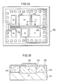
- the power supply lines 2 and the ground lines 3 are provided above the P+ separation regions 17.
- the ground lines 3 penetrate the silicon oxide film 20 along the longitudinal direction thereof and they are in ohmic contact with the P+ separation regions 17, so that the substrate 15 is stably set at a ground potential.
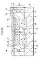
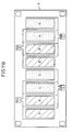
- Figs. 5B and 5C show schematic sectional views taken along the lines 5B-5B and 5C-5C in Fig. 5A, respectively.
- P ⁇ semiconductor substrate 15, an epitaxial N layer 16, P+ separation regions 17, N islands 18, burried N+ layers 19, a silicon oxide film 20 and an insulating film 21 of such as polyimide resin are formed in the same manner as in Fig. 3B.
- P+ diffusion regions 38 are formed on respective surfaces of N islands 18 and P diffusion regions 39 overlapping with main portions of the P+ regions 38 are further formed.
- the P regions 38 and 39 constitute the lower capacitor electrodes opposed to the upper capacitor electrodes 31 and they are connected to the respective connectors 36.
Landscapes
- Semiconductor Integrated Circuits (AREA)
- Design And Manufacture Of Integrated Circuits (AREA)
Applications Claiming Priority (24)
| Application Number | Priority Date | Filing Date | Title |
|---|---|---|---|
| JP153122/88 | 1988-06-21 | ||
| JP63153122A JPH0638452B2 (ja) | 1988-06-21 | 1988-06-21 | リニア半導体集積回路 |
| JP15312288 | 1988-06-21 | ||
| JP63173003A JPH0223659A (ja) | 1988-07-12 | 1988-07-12 | 半導体集積回路 |
| JP17301088 | 1988-07-12 | ||
| JP63173009A JP2675338B2 (ja) | 1988-07-12 | 1988-07-12 | 半導体集積回路 |
| JP173010/88 | 1988-07-12 | ||
| JP173003/88 | 1988-07-12 | ||
| JP173004/88 | 1988-07-12 | ||
| JP63173010A JPH0666415B2 (ja) | 1988-07-12 | 1988-07-12 | Fm/amチューナ用半導体集積回路 |
| JP173009/88 | 1988-07-12 | ||
| JP63173004A JPH0628285B2 (ja) | 1988-07-12 | 1988-07-12 | リニア半導体集積回路 |
| JP17300588 | 1988-07-12 | ||
| JP17300988 | 1988-07-12 | ||
| JP173005/88 | 1988-07-12 | ||
| JP63173005A JPH0648708B2 (ja) | 1988-07-12 | 1988-07-12 | 半導体集積回路 |
| JP17300388 | 1988-07-12 | ||
| JP17300488 | 1988-07-12 | ||
| JP202196/88 | 1988-08-12 | ||
| JP20219688A JPH0628289B2 (ja) | 1988-08-12 | 1988-08-12 | 半導体集積回路 |
| JP20219688 | 1988-08-12 | ||
| JP235828/88 | 1988-09-20 | ||
| JP63235828A JPH0719843B2 (ja) | 1988-09-20 | 1988-09-20 | 半導体集積回路 |
| JP23582888 | 1988-09-20 |
Publications (3)
| Publication Number | Publication Date |
|---|---|
| EP0347853A2 true EP0347853A2 (de) | 1989-12-27 |
| EP0347853A3 EP0347853A3 (de) | 1992-04-22 |
| EP0347853B1 EP0347853B1 (de) | 2000-02-02 |
Family
ID=27573235
Family Applications (1)
| Application Number | Title | Priority Date | Filing Date |
|---|---|---|---|
| EP89111233A Expired - Lifetime EP0347853B1 (de) | 1988-06-21 | 1989-06-20 | Integrierte Halbleiterschaltung |
Country Status (2)
| Country | Link |
|---|---|
| EP (1) | EP0347853B1 (de) |
| DE (1) | DE68929148T2 (de) |
Cited By (4)
| Publication number | Priority date | Publication date | Assignee | Title |
|---|---|---|---|---|
| EP0505248A1 (de) * | 1991-03-18 | 1992-09-23 | Fujitsu Limited | Verfahren zum Herstellen einer Halbleiteranordnung mit Schaltkreis-Blockeinheiten und damit hergestellte Halbleiteranordnungen |
| WO2006068286A1 (en) * | 2004-12-24 | 2006-06-29 | Semiconductor Energy Laboratory Co., Ltd. | Semiconductor device |
| US7906424B2 (en) | 2007-08-01 | 2011-03-15 | Advanced Micro Devices, Inc. | Conductor bump method and apparatus |
| US8314474B2 (en) | 2008-07-25 | 2012-11-20 | Ati Technologies Ulc | Under bump metallization for on-die capacitor |
Family Cites Families (1)
| Publication number | Priority date | Publication date | Assignee | Title |
|---|---|---|---|---|
| JPS492798B1 (de) * | 1969-04-16 | 1974-01-22 |
-
1989
- 1989-06-20 DE DE68929148T patent/DE68929148T2/de not_active Expired - Lifetime
- 1989-06-20 EP EP89111233A patent/EP0347853B1/de not_active Expired - Lifetime
Cited By (9)
| Publication number | Priority date | Publication date | Assignee | Title |
|---|---|---|---|---|
| EP0505248A1 (de) * | 1991-03-18 | 1992-09-23 | Fujitsu Limited | Verfahren zum Herstellen einer Halbleiteranordnung mit Schaltkreis-Blockeinheiten und damit hergestellte Halbleiteranordnungen |
| US5539224A (en) * | 1991-03-18 | 1996-07-23 | Fujitsu Limited | Semiconductor device having unit circuit-blocks in a common chip as a first layer with electrical interconnections therebetween provided exclusively in a second, upper, interconnection layer formed on the first layer |
| US5696013A (en) * | 1991-03-18 | 1997-12-09 | Fujitsu Limited | Method of manufacturing semiconductor device having unit circuit-blocks |
| WO2006068286A1 (en) * | 2004-12-24 | 2006-06-29 | Semiconductor Energy Laboratory Co., Ltd. | Semiconductor device |
| CN101088158B (zh) * | 2004-12-24 | 2010-06-23 | 株式会社半导体能源研究所 | 半导体装置 |
| US8716834B2 (en) | 2004-12-24 | 2014-05-06 | Semiconductor Energy Laboratory Co., Ltd. | Semiconductor device including antenna |
| US7906424B2 (en) | 2007-08-01 | 2011-03-15 | Advanced Micro Devices, Inc. | Conductor bump method and apparatus |
| US8294266B2 (en) | 2007-08-01 | 2012-10-23 | Advanced Micro Devices, Inc. | Conductor bump method and apparatus |
| US8314474B2 (en) | 2008-07-25 | 2012-11-20 | Ati Technologies Ulc | Under bump metallization for on-die capacitor |
Also Published As
| Publication number | Publication date |
|---|---|
| DE68929148T2 (de) | 2000-09-21 |
| EP0347853B1 (de) | 2000-02-02 |
| DE68929148D1 (de) | 2000-03-09 |
| EP0347853A3 (de) | 1992-04-22 |
Similar Documents
| Publication | Publication Date | Title |
|---|---|---|
| KR920005802B1 (ko) | 반도체 집적회로 | |
| US3373323A (en) | Planar semiconductor device with an incorporated shield member reducing feedback capacitance | |
| US5155570A (en) | Semiconductor integrated circuit having a pattern layout applicable to various custom ICs | |
| JPH0151065B2 (de) | ||
| EP0354512B1 (de) | Integrierte Halbleiterschaltung | |
| US5300798A (en) | Semiconductor integrated circuit device | |
| EP0347853B1 (de) | Integrierte Halbleiterschaltung | |
| KR930004982B1 (ko) | 반도체 집적회로 | |
| JPH0691226B2 (ja) | 半導体集積回路 | |
| JPH0638452B2 (ja) | リニア半導体集積回路 | |
| JPH0648708B2 (ja) | 半導体集積回路 | |
| JPH0474866B2 (de) | ||
| JPH0251253A (ja) | 半導体集積回路 | |
| JPH0719843B2 (ja) | 半導体集積回路 | |
| JP2675338B2 (ja) | 半導体集積回路 | |
| JPH0666414B2 (ja) | 半導体集積回路 | |
| JPH0628286B2 (ja) | リニア半導体集積回路 | |
| JPH0628285B2 (ja) | リニア半導体集積回路 | |
| JP2638544B2 (ja) | 半導体集積回路 | |
| JPH0652771B2 (ja) | リニア半導体集積回路 | |
| JPH0639454Y2 (ja) | 半導体集積回路 | |
| JPH0316163A (ja) | 半導体集積回路 | |
| JPH063840B2 (ja) | 半導体装置 | |
| JPH0628287B2 (ja) | リニア半導体集積回路 | |
| JPH1075146A (ja) | ノイズフィルタ |
Legal Events
| Date | Code | Title | Description |
|---|---|---|---|
| PUAI | Public reference made under article 153(3) epc to a published international application that has entered the european phase |
Free format text: ORIGINAL CODE: 0009012 |
|
| AK | Designated contracting states |
Kind code of ref document: A2 Designated state(s): DE FR GB |
|
| 17P | Request for examination filed |
Effective date: 19901228 |
|
| PUAL | Search report despatched |
Free format text: ORIGINAL CODE: 0009013 |
|
| AK | Designated contracting states |
Kind code of ref document: A3 Designated state(s): DE FR GB |
|
| 17Q | First examination report despatched |
Effective date: 19930708 |
|
| APAD | Appeal reference recorded |
Free format text: ORIGINAL CODE: EPIDOS REFNE |
|
| APAB | Appeal dossier modified |
Free format text: ORIGINAL CODE: EPIDOS NOAPE |
|
| GRAG | Despatch of communication of intention to grant |
Free format text: ORIGINAL CODE: EPIDOS AGRA |
|
| GRAH | Despatch of communication of intention to grant a patent |
Free format text: ORIGINAL CODE: EPIDOS IGRA |
|
| GRAH | Despatch of communication of intention to grant a patent |
Free format text: ORIGINAL CODE: EPIDOS IGRA |
|
| GRAH | Despatch of communication of intention to grant a patent |
Free format text: ORIGINAL CODE: EPIDOS IGRA |
|
| GRAA | (expected) grant |
Free format text: ORIGINAL CODE: 0009210 |
|
| AK | Designated contracting states |
Kind code of ref document: B1 Designated state(s): DE FR GB |
|
| REF | Corresponds to: |
Ref document number: 68929148 Country of ref document: DE Date of ref document: 20000309 |
|
| ET | Fr: translation filed | ||
| PLBE | No opposition filed within time limit |
Free format text: ORIGINAL CODE: 0009261 |
|
| STAA | Information on the status of an ep patent application or granted ep patent |
Free format text: STATUS: NO OPPOSITION FILED WITHIN TIME LIMIT |
|
| 26N | No opposition filed | ||
| REG | Reference to a national code |
Ref country code: GB Ref legal event code: IF02 |
|
| APAH | Appeal reference modified |
Free format text: ORIGINAL CODE: EPIDOSCREFNO |
|
| PGFP | Annual fee paid to national office [announced via postgrant information from national office to epo] |
Ref country code: DE Payment date: 20080626 Year of fee payment: 20 |
|
| PGFP | Annual fee paid to national office [announced via postgrant information from national office to epo] |
Ref country code: FR Payment date: 20080617 Year of fee payment: 20 |
|
| PGFP | Annual fee paid to national office [announced via postgrant information from national office to epo] |
Ref country code: GB Payment date: 20080625 Year of fee payment: 20 |
|
| REG | Reference to a national code |
Ref country code: GB Ref legal event code: PE20 Expiry date: 20090619 |
|
| PG25 | Lapsed in a contracting state [announced via postgrant information from national office to epo] |
Ref country code: GB Free format text: LAPSE BECAUSE OF EXPIRATION OF PROTECTION Effective date: 20090619 |