EP0347774A2 - Isolierungsschaltung und darin verwendetes dielektrisches Filter - Google Patents
Isolierungsschaltung und darin verwendetes dielektrisches Filter Download PDFInfo
- Publication number
- EP0347774A2 EP0347774A2 EP89110987A EP89110987A EP0347774A2 EP 0347774 A2 EP0347774 A2 EP 0347774A2 EP 89110987 A EP89110987 A EP 89110987A EP 89110987 A EP89110987 A EP 89110987A EP 0347774 A2 EP0347774 A2 EP 0347774A2
- Authority
- EP
- European Patent Office
- Prior art keywords
- resonator
- coupled
- conductive layer
- coupling
- resonators
- Prior art date
- Legal status (The legal status is an assumption and is not a legal conclusion. Google has not performed a legal analysis and makes no representation as to the accuracy of the status listed.)
- Granted
Links
- 230000008878 coupling Effects 0.000 claims description 68
- 238000010168 coupling process Methods 0.000 claims description 68
- 238000005859 coupling reaction Methods 0.000 claims description 68
- 239000003990 capacitor Substances 0.000 claims description 6
- 238000009413 insulation Methods 0.000 claims 1
- 239000004020 conductor Substances 0.000 description 10
- 230000002238 attenuated effect Effects 0.000 description 8
- 239000011159 matrix material Substances 0.000 description 8
- 239000002131 composite material Substances 0.000 description 6
- RYGMFSIKBFXOCR-UHFFFAOYSA-N Copper Chemical compound [Cu] RYGMFSIKBFXOCR-UHFFFAOYSA-N 0.000 description 3
- 229910052802 copper Inorganic materials 0.000 description 3
- 239000010949 copper Substances 0.000 description 3
- 239000003989 dielectric material Substances 0.000 description 3
- 229910052709 silver Inorganic materials 0.000 description 3
- 239000004332 silver Substances 0.000 description 3
- GWEVSGVZZGPLCZ-UHFFFAOYSA-N Titan oxide Chemical compound O=[Ti]=O GWEVSGVZZGPLCZ-UHFFFAOYSA-N 0.000 description 2
- 229910010293 ceramic material Inorganic materials 0.000 description 2
- 238000010586 diagram Methods 0.000 description 2
- 230000009191 jumping Effects 0.000 description 2
- 239000004743 Polypropylene Substances 0.000 description 1
- 230000006978 adaptation Effects 0.000 description 1
- 239000003822 epoxy resin Substances 0.000 description 1
- 238000002955 isolation Methods 0.000 description 1
- 238000012986 modification Methods 0.000 description 1
- 230000004048 modification Effects 0.000 description 1
- 229920000515 polycarbonate Polymers 0.000 description 1
- 239000004417 polycarbonate Substances 0.000 description 1
- 229920000647 polyepoxide Polymers 0.000 description 1
- -1 polypropylene Polymers 0.000 description 1
- 229920001155 polypropylene Polymers 0.000 description 1
- 229920005989 resin Polymers 0.000 description 1
- 239000011347 resin Substances 0.000 description 1
Images

Classifications
-
- H—ELECTRICITY
- H01—ELECTRIC ELEMENTS
- H01P—WAVEGUIDES; RESONATORS, LINES, OR OTHER DEVICES OF THE WAVEGUIDE TYPE
- H01P1/00—Auxiliary devices
- H01P1/20—Frequency-selective devices, e.g. filters
- H01P1/213—Frequency-selective devices, e.g. filters combining or separating two or more different frequencies
- H01P1/2136—Frequency-selective devices, e.g. filters combining or separating two or more different frequencies using comb or interdigital filters; using cascaded coaxial cavities
-
- H—ELECTRICITY
- H01—ELECTRIC ELEMENTS
- H01P—WAVEGUIDES; RESONATORS, LINES, OR OTHER DEVICES OF THE WAVEGUIDE TYPE
- H01P1/00—Auxiliary devices
- H01P1/20—Frequency-selective devices, e.g. filters
- H01P1/201—Filters for transverse electromagnetic waves
- H01P1/205—Comb or interdigital filters; Cascaded coaxial cavities
- H01P1/2056—Comb filters or interdigital filters with metallised resonator holes in a dielectric block
Definitions
- the present invention relates to an isolating circuit and a pair of dielectric filters for use therein, more particularly an isolating circuit, such as a duplexer or an isolator, for isolating a first frquency signal in a first frequency range and a second frequency signal is a second frequency range which is higher than the first frequency range, and still more particularly a duplexer well adapted for a mobile telephone.
- an isolating circuit such as a duplexer or an isolator
- the transmitting frequency band and receiving frequency band have respectively extended from 825-845 MHz to 824-849 MHz and from 870-890 MHz to 869-894MHz.
- a duplexer is required so as to more effectively isolate the transmitter and the receiver to permit simultaneous operation since the transmitting and receiving frequencies are more closely spaced.
- the dielectric filters which may be used in such duplexer are disclosed in Japanese laid-open patent publication Nos. 62-77703 (published on April 9th, 1987) and 62-157402 (published on July 13th, 1987).
- a dielectric filter disclosed in Japanese laid-open patent publication No. 62-77703, has six dielectric resonators therein and a reactance circuit formed by a capacitor or a inductor.
- the reactance circuit jumping over at least one resonator, connect two resonators out of the remaining resonators of the dielectric filter.
- the dielectric filters each have an attenuation pole.
- a dielectric filter disclosed in Japanese laid-open patent publication No. 62-157402, has four dielectric resonators therein and a coaxial cable having two edge portions.
- the coaxial cable jumping over two resonators, couple the two remaining resonators of the dielectric filter through two reactance components, respectively connected to two edge portions thereof.
- the dielectric filters have two attenuation poles which are asymnetric relative to the center frequency.
- An isolating circuit of the invention in order to isolate a first frequency signal in a first frequency range and a second frequency signal in a second frequency range which is higher than the first frequency range, has an antenna terminal, a first filter and a second filter.
- the first filter having a first input terminal and a first output terminal, is coupled to a first input signal including the first frequency signal at the first input terminal and attenuates first frequency compornents of the first input signal below the first frequency range at a first attenuation rate and a second frequency compornents of the first input signal above the first frequency range at a second attenuation rate.
- One of the first input and output terminals of the first filter is coupled to the antenna terminal.
- the first filter further has a first setting terminal setting the first attenuation rate and second attenuation rate so that the second attenuation rate is greater than the first attenuation rate.
- the second filter having second input and output terminals, is coupled to second input signal including the second frequency signal at the second input terminal and attenuates a third frequency compornents of the second input signal below the second frequency range at a third attenuation rate and a fourth frequency compornents of the second input signal above the second frequency range at a fourth attenuation rate.
- One of the second input and output terminals of the second filter is coupled to the antenna terminal.
- the second filter further has a second setting terminal setting the third attenuation rate and fourth attenuation rate so that the third attenuation rate is greater than the fourth attenuation rate.
- a dielectric filter in accordance with another aspect of the invention, includes a dielectric block having top, bottom, side surfaces and further a plurality of interior surfaces difining respective holes each extending from the top to bottom surfaces thereof.
- the filter has a side conductive layer covering the side surface, a bottom conductive layer covering said bottom surface electrically connected to the side layer, and first, second, third and fourth inner conductive layers respectively covering the interior surfaces and electrically connected to the bottom layer.
- the second inner layer is provided between the first and third inner layers and next to the first inner layer.
- the third inner layer is provided between the second and fourth inner layers and next to the fourth inner layer.
- the filter further has a first coupling terminal inductively and capacitively couples the first inner layer to the second inner layer.
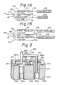
- FIGs. 1A and 1B there are respectively illustrated schematic diagrams of a duplexer 100 and an isolator 150 as two types of isolating circuits.
- the duplexer 100 comprises a transmitter filter 101 having an input terminal 103 and an output terminal 105, and a receiver filter 107 having an input terminal 109 and an output terminal 111.
- the output terminal 105 of the transmitter filter and the input terminal 109 of the receiver filter 107 are commonly coupled to an antenna terminal 113 through a connecting point 115.
- the transmitter filter 101 and receiver filter 107 are respectively supplied with the ground potential.
- the input terminal 103 of the transmitter filter 101, connected to a transmitter 102, and the output terminal 111 of the receiver filter 107, connected to a receiver 108, may be grounded through respective terminal resistors (not shown).
- the duplexer 100 In duplex operation of the transmitter 102 and the receiver 108 connected to a common antenna (not shown), the duplexer 100 is required so as to effectively isolate the transmitter 102 and the receiver 108 to permit simultaneous operation, especially, where the transmitting and receiving frequency signals are closely spaced.
- the transmitter filter 101 of the duplexer 100 is coupled to the transmitting frequency signals in a first frequency range from 824 HMz to 849 HMz and attenuates the other frequency signals in the other frequency range either below 824 MHz or above 849 MHz, while the receiver filter 107 is coupled to the receiving frequency signals in a second frequency range from 869 MHz to 894 HMz and attenuates the other frequency signals either below 869 HMz or above 894 HMz. Therefore, the duplexer 100 transmits the transmitting frequency signals from the transmitter 102 only into the antenna terminal 113 through the transmitter filter 101, and also transmits the receiving frequency signals from the antenna terminal 113 only into the receiver 108 through the receiver filter 107.
- the isolator 150 in Fig. 1B comprises a first receiver filter 151 having an input terminal 153 and an output terminal 155, and a second receiver filter 157 having an input terminal 159 and an output terminal 161.
- the input terminal 153 of the first receiver filter 151 and the input terminal 159 of the second receiver filter 157 are commonly coupled to an antenna terminal 163 through a connecting point 165.
- the first and second receiver filters 151 and 157 are respectively supplied with the ground potential.
- the respective output terminals 155 and 161 of the first and second receiver filters 151 and 157, respectively connected to first and second receiver, may be grounded through respective terminal resistors (not shown).
- the first receiver filter 151 is coupled to the first receiving frequency signals in a first frequency range and attenuates the other frequency signals in the other frequency range, while the second receiver filter 157 is coupled to the second receiving frequency signals in a second frequency range, higher than the first frequency range, and attenuates the other frequency signals. Therefore, the isolator 150 transmits the first receiving frequency signals from the antenna terminal 163 only into the first receiver 152 through the first receiver filter 151, and also transmits the second receiving frequency signals from the antenna terminal 163 only into the second receiver 158 through the second receiver filter 157.
- a first dielectric filter 200 which is applicable to either the transmitter filter 101 in Fig. 1A or the first receiver filter 151 in Fig. 1B.
- the first dielectric filter 200 includes a substantially rectangularly shaped block 210 of ceramic materials, primarily BaO and TiO2.
- the block has a top surface 211, a bottom surface 213, a pair of mutually parallel first side surfaces 215a and 215b and a pair of mutually parallel second side surfaces 217a and 217b.
- the block 210 further has four cylindrical interior surfaces therein which respectively define corresponding holes 219a, 219b, 219c and 219d each extending from the top surface 211 to the bottom surface 213 and arranged in a vertical plane to the first side surface 215a and 215b.
- Each of the interior surfaces in the block 210 is entirely covered with a layer of a conductive material such as a silver or copper so as to form inner conductive layers 221a, 221b, 221c and 221d.
- FIG. 3 there is illustrated a partially cross section of the first dielectric filter 200 shown in Fig. 2, substantially taken along lines A-A′.
- the inner conductive layers 221a-221d are electrically connected with one another by means of a bottom conductive layer 223 which may also be formed of silver or copper on the bottom surface 213 of the block 210.
- the bottom conductive layer 223 is electrically connected with similarly formed side conductive layers 225 provided on the side surfaces 215a, 215b, 217a and 217b.
- the first, second, third and fourth resonators 235a, 235b, 235c and 235d have respective top conductive layers 231a, 231b, 231c and 231d, shown in Figs 2 and 3.
- the top conductive layers 231a-231d respectively form collars covering the portions of the top surface 211 surrounding the four holes 219a-219d and are respectively connected to the corresponding inner conductive layers 221a- 221d.
- the block 210 further has first, second and third coupling conductive layers 241, 243 and 245 provided on the top surface 211 thereof.
- the second coupling conductive layer 243 connected to the side conductive layer 225 covering the first side surface 215a and 215b, is spaced from and provided between the top conductive layers 231c and 231d of the third an fourth resonators 235c and 235d in order to adjust the coupling frequencies between the third and fourth resonators 235c and 235d.
- each of the conductive layers 221, 223, 225, 231, 241, 243 and 245 is about 2 microns.
- the first dielectric filter 200 in Fig. 2 further employs first and second coupling terminals 250 and 260.
- the first and second coupling terminals 250 and 260 respectively have first and second "h"-shaped conductive parts 251 and 261 whose arms 251a and 261a respectively form the input and output terminals of either the transmitter filter 101 in Fig. 1A or the first receiver filter 151 in Fig. 1B.
- the first and second coupling terminals 250 and 260 each further includes two bushings 253a, 253b, 263a and 263b, made of dielectric materials such as polypropylene, polycarbonate, epoxy resin or ABC′ resin, and each having a thin round recess 271 therein.
- the legs 251b, 251c, 261b and 261c of the first and second conductive parts 251 and 261 are respectively fitted into the respective recesses 271 of bushings 253a, 253b, 263a and 263b.
- the bushings 253a, 253b, 263a and 263b are respectively fitted into the corresponding holes 219a, 219b, 219c and 219d so that the legs 251b, 251c, 261b and 261c of the first and second conductive parts 251 and 261 are respectively coupled with the corresponding inner conductive layers 221a, 221b, 221c and 221d.
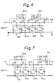
- FIG. 4 there is illustrated an equivalent circuit 400 of the dielectric filter 200 shown in Fig. 2.
- the equivalent circuit 400 has input and output terminals 411 and 413 formed by the respective arms 251a and 261a of the conductive parts 251 and 261 in Fig. 2, and first second, third and fourth resonator circuits 401, 403, 405 and 407 corresponding to the first, second, third and forth resonators 235a, 235b, 235c and 235d.
- Each resonator circuits 401, 403, 405 and 407 respectively formed by respective capacitances C1, C2, C3 and C4 and inductances L1, L2, L3 and L4, coupled to adjacent resonators by means of inductances L12, L23, L34 set up by the respective first, second and third coupling conductive layers 241, 243 and 245.
- the input terminal 411 is coupled to the first resonator circuit 401 through a capacitance C01 set up between the legs 251b of the first conductive part 21 and the inner conductor 221a through the bushing 253a, and further coupled to the second resonator circuit 403 through a inductor Lp1, set up by the first conductive part 251, and a composite capacitance Cp1 which is composed of the capacitance C01 and a capacitance set up between the legs 251c of the first conductive part 251 and the inner conductor 221b through the bushing 253b.
- While the output terminal 413 is coupled to the fourth resonator circuit 407 through a capacitance C02 set up between the legs 261b of the second conductive part 261 and the inner conductor 221d through the bushing 263a, and further coupled to the third resonator circuit 405 through a inductor Lp2, set up by the second conductive part 261, and a composite capacitance Cp2 which is composed of the capacitance C02 and a capacitance set up between the legs 261c of the second conductive part 261 and the inner conductor 221c through the bushing 263b.
- First and second coupling terminal circuits 409 and 410 composed of Cp1, Lp1, Cp2 and Lp2, are set up by the respective first and second coupling terminals 250 and 260.
- the above mentioned circuit 400 has first and second maximum values of the attenuation against first and second maximum attenuated frequency f ⁇ 1 and f ⁇ 2 near the first frequency range, that is, the pass band of the circuit 400 by means of the respective inductances L p 1 and L p 2 and composite capacitances C p 1 and C p 2, respectively set up by the first and second coupling terminal circuits 409 and 410 in Fig. 4.
- the first maximum value of the attenuation against the first maximum attenuated frequency f 1 set up by the first coupling terminal circuit 409 can be calculated in the following manner:
- the second maximum value of the attenuation against the second maximum attenuated frequency f ⁇ 2 can be calculated and will be found that f ⁇ 2 > f01.
- the first dielectric filter 200 having the equivalent circuit 400 has at least two maximum values of the attenuation above the center frequency f01 of the first frequency range (the pass band thereof).
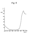
- Fig. 5 there is shown the attenuation volume according to the first dielectric filter 200 shown in Fig. 2 in the frequency range from 800 MHz to 880 MHz.
- the attenuation volume by the first dielectric filter 200 is significantly low level in the first frequency range from 824 MHz to 849 MHz, that is, the first dielectric filter 200 is coupled to the first signals in the first frequency range.
- the attenuation volume is increased at a first attenuation rate, while in the fourth frequency range above the first frequency range the attenuation volume is suddenly increased at a second attenuation rate which is greater than the first attenuation rate by means of the first and second coupling terminals 250 and 260 so as to significantly isolate the second frequency signals, coupled to another filter, in the second frequency range from 869 MHz to 894 MHz.
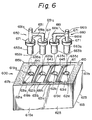
- a second dielectric filter 600 which is applicable to either the receiver filter 107 in Fig. 1A or the second receiver filter 157 in Fig. 1B.
- the second dielectric filter 600 being alike to the first dielectric filter 200 in Fig. 2 except for first, second and third coupling conductive layer 641, 643 and 645, includes a block 610 of ceramic materials.
- the block 610 has a top surface 611, a bottom surface 613, first side surfaces 615a and 615b, second side surfaces 617a and 617b and, further, four cylindrical interior surfaces therein which respectively define corresponding holes 619a, 619b, 619c and 619d each extending from the top surface 611 to the bottom surface 613.
- Each of the interior surfaces in the block 610 is entirely covered with a layer of a conductive material such as a silver or copper so as to form inner conductive layers 621a, 621b, 621c and 621d.
- the inner conductive layers 621a-621d are also electrically connected with one another by means of a bottom conductive layer 623 on the bottom surface 613.
- the bottom conductive layer 623 is electrically connected with a side conductive layer 625 provided on the side surfaces 615a, 615b, 617a and 617d.
- the first, second, third and fourth resonators 635a-635d have respective top conductive layers 631a, 631b, 631c and 631d, respectively connected with the corresponding inner conductive layers 621a-621d on the top surface 611.
- the block 610 further has the first, second and third coupling conductive layers 641, 643 and 645 spaced from the provided between the side conductive layer 625 covering the first side surfaces 615a and 615b on the top surface 611 thereof.
- the first coupling conductive layer 641 is spaced from and provided between the top conductive layers 631a and 631b in order to adjust the coupling frequencies between the first and second resonators 635a and 635b.
- the second conductive layer 643 is spaced from and provided between the top conductive layers 231b and 231c of the second and third resonators 635b and 635c in order to adjust the coupling frequencies between the second and third resonators.
- the third coupling conductive layer 645 is also spaced from and provided between the top conductive layers 631c and 631d of the third and fourth resonators 635c and 635d in order to adjust the coupling frequencies between the third and fourth resonators 635c and 635d.
- the second dielectric filter 600 in Fig. 6 further employs first and second coupling terminals 650 and 660.
- the first and second coupling terminals 650 and 660 respectively have first and second "h"-shaped conductive parts 650 and 661 whose arms 651a and 661a respectively form the input and output terminals of either the receiver filter 107 in Fig. 1A or the second receiver filter 157 in Fig. 1B.
- the first and second coupling terminals 650 and 660 each further includes two bushings 653a, 653b, 663a and 663b each having a thin round recess 671 therein.
- the legs 651b, 651c, 661b and 661c of the first and second conductive parts 651 and 661 are respectively fitted into the respective recesses 671 of bushings 653a, 653b, 663a and 663b.
- the bushings 653a, 653b, 663a and 663b are further respectively fitted into the corresponding holes 619a, 619b, 619c and 619d so that the legs 651b, 651c, 661b and 661c of the first and second conductive parts 651 and 661 are respectively coupled with the corresponding inner conductive layers 621a-621d.
- FIG. 7 there is illustrated an equivalent circuit 700 of the second dielectric filter 600 shown in Fig. 6.
- the equivalent circuit 700 has input and output terminals 711 and 713 formed by the respective arms 651a and 661a of the conductive parts 651 and 661 in Fig. 6, and first, second, third and fourth resonator circuits 701, 703, 705 and 707 corresponding to the first, second, third and fourth resonators 635a, 635b, 635c and 635d.
- Each resonator circuits 701, 703, 705 and 707 respectively formed by respective capacitances C1 , C2, C3 and C4 and inductances L1, L2, L3 and L4, coupled to adjacent resonators by means of capacitance C12, C23, C34 set up by the respective first, second and third coupling conductive layers 241, 243 and 245.
- the input terminal 711 is coupled to the first resonator circuit 701 through a capacitance C01 set up between the legs 651b of the first conductive part 651 and the inner conductor 621a through the bushing 653a, and further coupled to the second resonator circuit 403 through a inductor L p 1, set up by the first conductive part 651, and a composite capacitance C p 1 which is composed of the capacitance C01 and a capacitance set up between the legs 651c of the first conductive part 651 and the inner conductor 621b through the bushing 653b.
- While the output terminal 713 is coupled to the fourth resonator circuit 707 through a capacitance C02 set up between the legs 661b of the second conductive part 661 and the inner conductor 621d through the bushing 663a, and further coupled to the third resonator circuit 705 through a inductor L p 2, set up by the second conductive part 661, and a composite capacitance C p 2 which is composed of the capacitance C02 and a capacitance set up between the legs 661c of the second conductive part 661 and the inner conductor 621c through the bushing 663b.
- First and second coupling terminal circuits 709 and 710 composed of L p 1, C p 1, L p 2 and C p 2, is set up by the respective first and second coupling terminals 650 and 660.
- the above mentioned circuit 700 has first and second maximum values of the attenuation near the second frequency rage, that is the pass band of the circuit 700 by means of the respective inductances L p 1 and L p 2 and composite capacitances C p 1 and C p 2, respectively set up by the first and second coupling terminal circuits 709 and 710 in Fig. 7.
- the first maximum value of the attenuation set up by the first coupling terminal circuit 709 can be calculated in the following manner:
- the second maximum value of the attenuation against the second maximum attenuated frequency f ⁇ 2 can be calculated and will be found that f ⁇ 2 ⁇ f02.
- the second dielectric filter 600 having the equivalent circuit 700 has at least two maximum values of the attenuation below the center frequency f02 of the second frequency range (the pass band thereof).
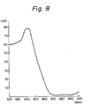
- Fig. 8 there is shown the attenuation volume according to the second dielectric filter 600 shown in Fig. 6 in the frequency range from 820 HMz to 900 lfHmz.
- the attenuation volume by the second dielectric filter 600 is significantly low level in the second frequency range from 869 HMz to 894 HMz, that is, the second dielectric filter 600 is coupled to the second signals in the second frequency range.
- the attenuation volume is suddenly increased at a third attenuation rate, while in the sixth frequency range above the second frequency range the attenuation volume is increased at a fourth attenuation rate.
- the third attenuation rate is greater than the fourth attenuation rate by means of the first and second coupling terminals 650 and 660 so as to significantly isolate the first frequency signals, coupled to the first dielectric filter, in the first frequency range from 824 MHz to 849 HMz.
- both of the first and second dielectric filter 200 and 600 can respectively have at least one maximum value of attenuation in the range above the first frequency range and below the second frequency range if each of the first and second dielectric filter 200 and 600 has at least one coupling terminals which couples either the first resonator to the second (adjacent) resonator or the fourth (final) resonator to the third (adjacent) resonator.
- the isolating circuit, composed of such first and second dielectric filter should sufficiently isolate the first and second frequency signals.
Landscapes
- Physics & Mathematics (AREA)
- Electromagnetism (AREA)
- Control Of Motors That Do Not Use Commutators (AREA)
Applications Claiming Priority (4)
| Application Number | Priority Date | Filing Date | Title |
|---|---|---|---|
| JP150136/88 | 1988-06-20 | ||
| JP15013688A JPH01318401A (ja) | 1988-06-20 | 1988-06-20 | 有極型誘電体フィルタ |
| JP218475/88 | 1988-09-02 | ||
| JP21847588A JPH0267801A (ja) | 1988-09-02 | 1988-09-02 | 有極型誘電体フィルタ |
Publications (3)
| Publication Number | Publication Date |
|---|---|
| EP0347774A2 true EP0347774A2 (de) | 1989-12-27 |
| EP0347774A3 EP0347774A3 (en) | 1990-11-22 |
| EP0347774B1 EP0347774B1 (de) | 1995-11-22 |
Family
ID=26479833
Family Applications (1)
| Application Number | Title | Priority Date | Filing Date |
|---|---|---|---|
| EP89110987A Expired - Lifetime EP0347774B1 (de) | 1988-06-20 | 1989-06-16 | Isolierungsschaltung und darin verwendetes dielektrisches Filter |
Country Status (3)
| Country | Link |
|---|---|
| US (1) | US5015974A (de) |
| EP (1) | EP0347774B1 (de) |
| DE (1) | DE68924873T2 (de) |
Cited By (4)
| Publication number | Priority date | Publication date | Assignee | Title |
|---|---|---|---|---|
| EP0442418A3 (en) * | 1990-02-14 | 1992-09-16 | Oki Electric Industry Company, Limited | Dielectric filter having coupling amount adjusting patterns |
| US5227747A (en) * | 1989-06-15 | 1993-07-13 | Oki Electric Industry Co., Ltd. | Dielectric filter having coupling amount adjusting patterns |
| EP1009059A1 (de) * | 1998-12-10 | 2000-06-14 | Ngk Spark Plug Co., Ltd | Dielektrisches Filter mit regelbarer Frequenzbandbreite |
| US12176651B2 (en) | 2020-06-18 | 2024-12-24 | Ideal Industries, Inc. | Conductor terminal |
Families Citing this family (4)
| Publication number | Priority date | Publication date | Assignee | Title |
|---|---|---|---|---|
| US5229729A (en) * | 1989-12-14 | 1993-07-20 | Murata Manufacturing Co., Ltd. | Radio frequency signal combining/sorting apparatus |
| FI88441C (fi) * | 1991-06-25 | 1993-05-10 | Lk Products Oy | Temperaturkompenserat dielektriskt filter |
| US7903679B1 (en) * | 2006-04-11 | 2011-03-08 | Altera Corporation | Power supply filtering for programmable logic device having heterogeneous serial interface architecture |
| US10333191B2 (en) | 2016-09-23 | 2019-06-25 | Cts Corporation | Ceramic block RF filter having a first plurality of through-hole resonators and a second plurality of through-holes for blocking RF signal coupling |
Family Cites Families (17)
| Publication number | Priority date | Publication date | Assignee | Title |
|---|---|---|---|---|
| JPS5657302A (en) * | 1979-10-15 | 1981-05-19 | Murata Mfg Co Ltd | Microwave device using coaxial resonator |
| JPS5679502A (en) * | 1979-11-30 | 1981-06-30 | Matsushita Electric Ind Co Ltd | Band block filter and antenna duplexer |
| JPS60114004A (ja) * | 1983-11-25 | 1985-06-20 | Murata Mfg Co Ltd | 誘電体フィルタの実装構造 |
| GB2165098B (en) * | 1984-09-27 | 1988-05-25 | Motorola Inc | Radio frequency filters |
| US4742562A (en) * | 1984-09-27 | 1988-05-03 | Motorola, Inc. | Single-block dual-passband ceramic filter useable with a transceiver |
| US4768003A (en) * | 1984-09-28 | 1988-08-30 | Oki Electric Industry Co., Inc. | Microwave filter |
| JPS61214625A (ja) * | 1985-03-19 | 1986-09-24 | Tokyo Electric Co Ltd | アンテナ結合回路 |
| JPS6218801A (ja) * | 1985-07-17 | 1987-01-27 | Murata Mfg Co Ltd | 誘電体フイルタ |
| JPS62157402A (ja) * | 1985-12-27 | 1987-07-13 | Murata Mfg Co Ltd | 誘電体フイルタ |
| US4740765A (en) * | 1985-09-30 | 1988-04-26 | Murata Manufacturing Co., Ltd. | Dielectric filter |
| JPS6277703A (ja) * | 1985-09-30 | 1987-04-09 | Murata Mfg Co Ltd | 誘電体フイルタ |
| JPH0793522B2 (ja) * | 1986-04-12 | 1995-10-09 | ティーディーケイ株式会社 | 誘電体フィルタの位相調整装置 |
| JPS63961A (ja) * | 1986-06-18 | 1988-01-05 | Matsushita Electric Ind Co Ltd | 有機電解質電池 |
| US4692726A (en) * | 1986-07-25 | 1987-09-08 | Motorola, Inc. | Multiple resonator dielectric filter |
| JPS6342201A (ja) * | 1986-08-07 | 1988-02-23 | Alps Electric Co Ltd | マイクロ波分波器 |
| JPS63124601A (ja) * | 1986-11-14 | 1988-05-28 | Oki Electric Ind Co Ltd | 誘電体フイルタ |
| JPS63174402A (ja) * | 1987-01-13 | 1988-07-18 | Murata Mfg Co Ltd | 誘電体フイルタ装置 |
-
1989
- 1989-06-15 US US07/366,516 patent/US5015974A/en not_active Expired - Fee Related
- 1989-06-16 DE DE68924873T patent/DE68924873T2/de not_active Expired - Fee Related
- 1989-06-16 EP EP89110987A patent/EP0347774B1/de not_active Expired - Lifetime
Cited By (5)
| Publication number | Priority date | Publication date | Assignee | Title |
|---|---|---|---|---|
| US5227747A (en) * | 1989-06-15 | 1993-07-13 | Oki Electric Industry Co., Ltd. | Dielectric filter having coupling amount adjusting patterns |
| EP0442418A3 (en) * | 1990-02-14 | 1992-09-16 | Oki Electric Industry Company, Limited | Dielectric filter having coupling amount adjusting patterns |
| EP1009059A1 (de) * | 1998-12-10 | 2000-06-14 | Ngk Spark Plug Co., Ltd | Dielektrisches Filter mit regelbarer Frequenzbandbreite |
| US6304159B1 (en) | 1998-12-10 | 2001-10-16 | Ngk Spark Plug Co., Ltd. | Dielectric filter with adjustable frequency bandwidth |
| US12176651B2 (en) | 2020-06-18 | 2024-12-24 | Ideal Industries, Inc. | Conductor terminal |
Also Published As
| Publication number | Publication date |
|---|---|
| DE68924873T2 (de) | 1996-05-02 |
| DE68924873D1 (de) | 1996-01-04 |
| EP0347774A3 (en) | 1990-11-22 |
| EP0347774B1 (de) | 1995-11-22 |
| US5015974A (en) | 1991-05-14 |
Similar Documents
| Publication | Publication Date | Title |
|---|---|---|
| US6542050B1 (en) | Transmitter-receiver | |
| US5293141A (en) | Dielectric filter having external connection terminals on dielectric substrate and antenna duplexer using the same | |
| US7023301B2 (en) | Laminated filter with a single shield conductor, integrated device, and communication apparatus | |
| CA2116375A1 (en) | Radio frequency filter | |
| US5686873A (en) | Antenna duplexer having transmit and receive portion formed in a single dielectric block | |
| US5015973A (en) | Duplexer with an isolating circuit on a dielectric plate | |
| EP0347774A2 (de) | Isolierungsschaltung und darin verwendetes dielektrisches Filter | |
| US5486799A (en) | Strip line filter and duplexer filter using the same | |
| JP2764903B2 (ja) | 複数共振器要素‐実装可能フィルタ | |
| US6989725B2 (en) | Dielectric resonator, dielectric filter, dielectric duplexer, and communication apparatus incorporating the same | |
| US20020135438A1 (en) | Filter unit and duplexer comprising such filter units | |
| JPH08191230A (ja) | 分波器 | |
| US6677836B2 (en) | Dielectric filter device having conductive strip removed for improved filter characteristics | |
| US6008707A (en) | Antenna duplexer | |
| US5712604A (en) | Dielectric filter including at least one band elimination filter | |
| US7183878B2 (en) | Surface acoustic wave filter | |
| KR100449226B1 (ko) | 유전체 듀플렉서 | |
| US6504452B2 (en) | Low-pass filter and mobile communication device using the same | |
| EP0704924B1 (de) | Dielektrisches Filter | |
| KR100401966B1 (ko) | 복합 유전체 필터 장치 및 이를 결합한 통신 장치 | |
| KR100550878B1 (ko) | 적층형 유전체 필터 | |
| KR100456004B1 (ko) | 듀플렉서의 송신대역 통과필터 | |
| JPH08111604A (ja) | 誘電体フィルタ | |
| KR100388051B1 (ko) | 일체형 이중대역 듀플렉서 | |
| JPH08154004A (ja) | 誘電体フィルタ |
Legal Events
| Date | Code | Title | Description |
|---|---|---|---|
| PUAI | Public reference made under article 153(3) epc to a published international application that has entered the european phase |
Free format text: ORIGINAL CODE: 0009012 |
|
| AK | Designated contracting states |
Kind code of ref document: A2 Designated state(s): DE FR GB SE |
|
| PUAL | Search report despatched |
Free format text: ORIGINAL CODE: 0009013 |
|
| AK | Designated contracting states |
Kind code of ref document: A3 Designated state(s): DE FR GB SE |
|
| 17P | Request for examination filed |
Effective date: 19901228 |
|
| 17Q | First examination report despatched |
Effective date: 19930405 |
|
| GRAA | (expected) grant |
Free format text: ORIGINAL CODE: 0009210 |
|
| AK | Designated contracting states |
Kind code of ref document: B1 Designated state(s): DE FR GB SE |
|
| ET | Fr: translation filed | ||
| REF | Corresponds to: |
Ref document number: 68924873 Country of ref document: DE Date of ref document: 19960104 |
|
| PLBE | No opposition filed within time limit |
Free format text: ORIGINAL CODE: 0009261 |
|
| STAA | Information on the status of an ep patent application or granted ep patent |
Free format text: STATUS: NO OPPOSITION FILED WITHIN TIME LIMIT |
|
| 26N | No opposition filed | ||
| PGFP | Annual fee paid to national office [announced via postgrant information from national office to epo] |
Ref country code: GB Payment date: 19980608 Year of fee payment: 10 |
|
| PGFP | Annual fee paid to national office [announced via postgrant information from national office to epo] |
Ref country code: FR Payment date: 19980609 Year of fee payment: 10 |
|
| PGFP | Annual fee paid to national office [announced via postgrant information from national office to epo] |
Ref country code: SE Payment date: 19980616 Year of fee payment: 10 |
|
| PGFP | Annual fee paid to national office [announced via postgrant information from national office to epo] |
Ref country code: DE Payment date: 19980622 Year of fee payment: 10 |
|
| PG25 | Lapsed in a contracting state [announced via postgrant information from national office to epo] |
Ref country code: GB Free format text: LAPSE BECAUSE OF NON-PAYMENT OF DUE FEES Effective date: 19990616 |
|
| PG25 | Lapsed in a contracting state [announced via postgrant information from national office to epo] |
Ref country code: SE Free format text: THE PATENT HAS BEEN ANNULLED BY A DECISION OF A NATIONAL AUTHORITY Effective date: 19990629 |
|
| PG25 | Lapsed in a contracting state [announced via postgrant information from national office to epo] |
Ref country code: FR Free format text: THE PATENT HAS BEEN ANNULLED BY A DECISION OF A NATIONAL AUTHORITY Effective date: 19990630 |
|
| GBPC | Gb: european patent ceased through non-payment of renewal fee |
Effective date: 19990616 |
|
| EUG | Se: european patent has lapsed |
Ref document number: 89110987.8 |
|
| PG25 | Lapsed in a contracting state [announced via postgrant information from national office to epo] |
Ref country code: DE Free format text: LAPSE BECAUSE OF NON-PAYMENT OF DUE FEES Effective date: 20000503 |
|
| REG | Reference to a national code |
Ref country code: FR Ref legal event code: ST |