EP0343871B1 - Münzprüfer - Google Patents
Münzprüfer Download PDFInfo
- Publication number
- EP0343871B1 EP0343871B1 EP89305093A EP89305093A EP0343871B1 EP 0343871 B1 EP0343871 B1 EP 0343871B1 EP 89305093 A EP89305093 A EP 89305093A EP 89305093 A EP89305093 A EP 89305093A EP 0343871 B1 EP0343871 B1 EP 0343871B1
- Authority
- EP
- European Patent Office
- Prior art keywords
- coin
- detecting
- adder
- pattern
- output
- Prior art date
- Legal status (The legal status is an assumption and is not a legal conclusion. Google has not performed a legal analysis and makes no representation as to the accuracy of the status listed.)
- Expired - Lifetime
Links
- 239000006185 dispersion Substances 0.000 claims description 7
- 239000000872 buffer Substances 0.000 claims description 5
- 230000003111 delayed effect Effects 0.000 claims description 3
- 230000000712 assembly Effects 0.000 description 14
- 238000000429 assembly Methods 0.000 description 14
- 239000003990 capacitor Substances 0.000 description 8
- 239000000463 material Substances 0.000 description 6
- 230000010355 oscillation Effects 0.000 description 6
- 238000000034 method Methods 0.000 description 5
- 238000001514 detection method Methods 0.000 description 4
- 230000003068 static effect Effects 0.000 description 4
- 238000010586 diagram Methods 0.000 description 3
- 238000010200 validation analysis Methods 0.000 description 2
- 230000002238 attenuated effect Effects 0.000 description 1
- 238000005452 bending Methods 0.000 description 1
- 230000007423 decrease Effects 0.000 description 1
- 230000008021 deposition Effects 0.000 description 1
- 238000006073 displacement reaction Methods 0.000 description 1
- 239000000428 dust Substances 0.000 description 1
- 238000005259 measurement Methods 0.000 description 1
Images


Classifications
-
- G—PHYSICS
- G07—CHECKING-DEVICES
- G07D—HANDLING OF COINS OR VALUABLE PAPERS, e.g. TESTING, SORTING BY DENOMINATIONS, COUNTING, DISPENSING, CHANGING OR DEPOSITING
- G07D5/00—Testing specially adapted to determine the identity or genuineness of coins, e.g. for segregating coins which are unacceptable or alien to a currency
- G07D5/08—Testing the magnetic or electric properties
-
- G—PHYSICS
- G07—CHECKING-DEVICES
- G07D—HANDLING OF COINS OR VALUABLE PAPERS, e.g. TESTING, SORTING BY DENOMINATIONS, COUNTING, DISPENSING, CHANGING OR DEPOSITING
- G07D5/00—Testing specially adapted to determine the identity or genuineness of coins, e.g. for segregating coins which are unacceptable or alien to a currency
- G07D5/02—Testing the dimensions, e.g. thickness, diameter; Testing the deformation
-
- G—PHYSICS
- G07—CHECKING-DEVICES
- G07D—HANDLING OF COINS OR VALUABLE PAPERS, e.g. TESTING, SORTING BY DENOMINATIONS, COUNTING, DISPENSING, CHANGING OR DEPOSITING
- G07D5/00—Testing specially adapted to determine the identity or genuineness of coins, e.g. for segregating coins which are unacceptable or alien to a currency
- G07D5/005—Testing the surface pattern, e.g. relief
Definitions
- This invention relates to coin validators used in various automatic service devices of a bending machine or the like, and more particularly to such validators which discern the thickness and/or patterns of coins in a non-contact manner.
- Electronic coin validators used very often today include an oscillator coil disposed on one side of a coin path and a receiver coil disposed on the other side of the coin path and coupled electromagnetically to the oscillator coil to detect the outer shape and material of a coin during its passage to determine the validation and kind of the coin in accordance with an attenuated waveform of a voltage output by the receiver coil.
- These validators are suitable for detecting the diameter and material of a coin using the oscillator and receiver coil, but are not suitable for detecting the thickness and pattern of the coins. If these validators detect the thickness and pattern of a coin, a signal containing a component depending on the material of the coin appears in the receiver coil output, so that it is necessary to provide a circuit to eliminate signal components depending on the coin material for this material, and hence the structure of the validator would be complicated. In order to respond to a change in the thickness of its details such as a pattern, the coin must be stopped temporarily, or an extremely high speed circuit unit must be used, so that the mechanism and circuit structure would be complicated. It is impossible to discern a false coin, especially, of the same material and shape as a genuine one using such selective method.
- the face of a false coin is flat while the face of a genuine coin has a rugged pattern and an uneven thickness.
- a method of selecting a coin in accordance with a varying electrode capacitance due to a rugged face or appearance of the coin, namely, caused by inserting the coin between a pair of electrode plates, is disclosed, for example, in Japanese Published Examined Patent Application Sho 39-21291.
- the static capacitance present between the pair of electrode plates changes.
- Such pair of electrode plates are connected as one of the elements of a capacitor bridge or as one of oscillating elements of an oscillator to thereby select a coin using an unbalance in the capacitor bridge or an oscillation or non-oscillation of the oscillator.
- the electrode structure includes a mere arrangement of two opposing electrode plates, the electric lines of force from the electrode plates are dispersed, so that a fine change in the rugged face of the coin cannot be detected, and secure detection cannot be achieved.
- DE-A-1 673 841 discloses the use of guard rings surrounding sensor electrodes to guide the lines of force from the electrodes.
- the present invention provides a coin validator having a first sensor electrode disposed on one side of a coin path and a second sensor electrode disposed on the other side of the coin path so as to oppose the first sensor electrode, for discriminating a type of a coin passing through the coin path in accordance with a change in capacitance between the first sensor electrode and the second sensor electrode, characterized by: a first guard ring electrode provided so as to surround the first sensor electrode for preventing the dispersion of electric lines of force generated by the first sensor electrode; a second guard ring electrode provided so as to surround the second sensor electrode for preventing the dispersion of electric lines of force generated by the second sensor electrode; an oscillator for outputting an oscillating signal of a predetermined frequency; a resonator resonating with the oscillating signal from the oscillator for applying a resonating output therefrom to at least one of the first and second sensor electrodes; and coin discriminating means for discriminating the type of the coin in accordance with the output signal voltage from the resonator during
- the electrodes disposed on the corresponding sides of the coin path namely, the first and second sensor electrodes which detect a change in the inter-electrode capacitance generated during coin passage, and the first and second guard ring electrodes which prevent the dispersion of the eletric lines of force generated by the first and second sensor electrodes apply across the coin path the electric lines of force due to a resonating output signal.
- the static capacitance between the electrode assemblies changes to thereby change the resonating output voltage. This change follows a change in the thickness and/or pattern of the coin.
- the thickness and/or pattern of the coin are detected by a voltage or waveform indicative of this change. If the change in the resonating output voltage signal is within a range of a predetermined reference voltage, the coin is confirmed to be within an allowable predetermined thickness condition. If an output waveform is generated which crosses a predetermined voltage level several times, the coin is considered to fluctuate within a predetermined thickness range and can be determined to "have a pattern". In this case, the electric lines of force from the sensor electrodes are focused into a beam by the guard ring electrodes, so that the thickness of the coin can be detected finely.
- arrangement is such that the thickness and/or pattern of a coin is detected using a change in the static capacitance on the pair of electrode assemblies, and the magnitude of a change of and the waveform of the resonating voltage due to the change in the static capacitance. Therefore, the thickness and/or pattern of the coin is discerned with high reliability.
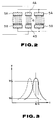
- Fig. 1 is a circuit diagram of an embodiment of a coin validator according to the present invention.
- a pair of opposing electrode assemblies 2 and 3 are disposed on the corresponding sides of a coin path so as to face the front and back faces of a coin 1.
- these electrode assemblies 2 and 3 are constituted by sensor electrodes 4A and 4B disposed at a center, and guard ring electrodes 5A and 5B disposed so as to surround the corresponding sensor electrodes in order to prevent the dispersion of the electric lines of force 6 from the sensor electrodes 4A and 4B, respectively.
- the sensor electrodes 4A and 4B are impressed with the output signals from resonators 7 and 8 which resonate with a resonating frequency f0 determined by coils L1 and L2, capacitors C1 and C2 and stray capacitances C1f and C2f including the capacitances inherent to the electrode assemblies 2 and 3, respectively.
- the resonator 7 receives an oscillation signal from an oscillator 9 which oscillates at a frequency f1 while the resonator 8 receives an oscillation signal comprising an inverse of the oscillation signal from the oscillator 9 and supplied via an invertor 10 and having an inverted polarity.
- the oscillation frequency f1 is set to a value higher than the resonating frequency f0.
- the outputs of the capacitances C1 and C2 are connected to the corresponding sensor electrodes 4A and 4B and also connected to the inputs of buffers 11 and 12, the outputs of which are applied to the guard ring electrodes 5A and 5B of the electrode assemblies 2 and 3 so as to prevent the dispersion of the electric lines of force 6 across the sensor electrodes 4A and 4B as shown in Fig. 2.
- the outputs of the buffers 11 and 12 are connected to detecting and rectifying circuits 13 and 14, respectively, where the signal components centered at the frequency f0 are changed into DC voltages, which are then added in an adder 15.
- the output of the adder 15 is then input to a thickness detector 16 and a pattern detector 17.
- the thickness detector 16 determines whether the thickness of the coin is appropriate by detecting whether a fluctuation of the voltage output from the adder 15 generated when the coin passes between the electrode assemblies is in a range corresponding to an appropriate thickness condition.
- the pattern detector 17 detects the presence of a pattern depending on whether the fluctuation of the output voltage signal from the adder 15 is in a waveform range corresponding to the pattern of the coin. The results of the detections are delivered to a controller 18 where the validation and kind of the coin are determined.
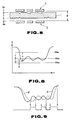
- a voltage V1 is generated at a frequency f1 across each of the capacitors C1 and C2 as shown in Fig. 3.
- the frequency f0 is the resonant frequency in the standby state.
- the capacitance between the electrode assemblies 2 and 3 changes during passage of the coin 1, so that the curve on the resonating waveform shown in Fig. 3 moves from the position shown by the solid line to the position shown by the broken lines on a lower frequency side.
- the voltage across the capacitors C1 and C2 decreases from V1 to V2.
- a change in the capacitance during passage of the coin is small, for example, 0.1 pF or less, but that small change can be extracted as a large change in the voltage amplitude because the resonating frequency deviates.
- Changes in the voltages across the capacitors C1 and C2 are detected and rectified by the detecting and rectifying circuits 13 and 14 via the buffers 11 and 12 into the waveforms a (solid line) and b (broken line) shown in Fig. 4. As shown in Fig.
- the waveform c (dot-dashed line) comprising the addition of the waveforms a (solid line) and b (broken line) in Fig. 4 has a correlation to the thickness of the coin (microscopically, the pattern on each of the faces of the coin) as obtained from the above equation. Namely, if the waveform c is used, the thickness of the coin 1 having passed between the electrode assemblies 2 and 3 can be detected even if the coin 1 passes closer to the electrode assembly 2 than to the electrode assembly 3 and vice verse.
- the details of the thickness detector 16 are not shown. As shown in Fig. 4, a comparator or the like is used to detect whether the bottom of the waveform c is between set reference voltages Vth1 and Vth2. While the details of the pattern detector 17 are not shown, a reference voltage Vth3 is set as shown in Fig. 6 and the determination "there is a pattern" is done if the bottom of the waveform c crosses Vth3 three times or more. With a false coin without patterns, the output waveform c of the adder 15 is shown by d (solid line) or e (broken line) in Fig. 7 and does not cross Vth3 three times or more. Therefore, it is determined that the coin has no patterns.
- Vth1, Vth2, Vth3 may be set variably as follows. As shown in Fig. 8, Vth1, Vth2 and Vth3 are set at levels shifted by particular respective voltages ( ⁇ , ⁇ , ⁇ ) with reference to the minimum fall voltage level of the output waveform c from the adder 15. By such setting, the thickness and/or pattern of the coin can be detected surely even if the ambient conditions change due to humidity and/or deposition of dust.
- a pulse waveform corresponding to the ruggedness of the pattern is extracted, and the presence of the pattern can be detected using the number and width of pulses in the pulse waveform without using Vth3, as shown in Fig. 9.
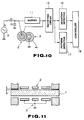
- the thickness and pattern of a coin can be detected by grounding the electrode assembly 3 at 0V by using a change in the output voltage from the capacitor C1 due to a change in the capacitance between the coin 1 and the electrode assembly 2 as shown in Fig. 10.
- the thickness detector 16 is required to function as a displacement detector 16′ and the pattern detector 17 is required to function as a circuit to detect a pattern on one of the coin faces. It is necessary to set the relative relationship between the coin 1 and the electrode assembly 2 such that they have a constant distance D therebetween as shown in Fig. 11. This can be easily realized by inclining the coin path toward the electrode assembly 2 or 3.
Landscapes
- Physics & Mathematics (AREA)
- General Physics & Mathematics (AREA)
- Testing Of Coins (AREA)
- Measurement Of Length, Angles, Or The Like Using Electric Or Magnetic Means (AREA)
Claims (13)
- Münzprüfer mit einer ersten Sensorelektrode (4A), die auf einer Seite einer Münzbahn angeordnet ist, und einer zweiten Sensorelektrode (4B), die auf der anderen Seite der Münzbahn derart angeordnet ist, daß sie der ersten Sensorelektrode gegenüberliegt, zum Bestimmen der Art einer die Münzbahn passierenden Münze entsprechend einer Kapazitätsänderung zwischen der ersten Sensorelektrode und der zweiten Sensorelektrode, gekennzeichnet durch:
eine erste Schutzringelektrode (5A), die derart vorgesehen ist, daß sie die erste Sensorelektrode umgibt, um die Streuung von von der ersten Sensorelektrode erzeugten elektrischen Kraftlinien (6) zu unterbinden;
eine zweite Schutzringelektrode (5B), die derart vorgesehen ist, daß sie die zweite Sensorelektrode umgibt, um die Streuung von von der zweiten Sensorelektrode erzeugten elektrischen Kraftlinien (6) zu unterbinden;
einen Oszillator (9) zum Abgeben eines Oszillationssignals mit einer vorbestimmten Frequenz;
einen Resonator (7, 10, 8), der mit dem Oszillationssignal von dem Oszillator resoniert, um ein Resonationsausgangssignal davon mindestens an eine der ersten und der zweiten Sensorelektrode zu geben; und
eine Münzbestimmungseinrichtung (13-18) zum Bestimmen des Typs der Münze entsprechend der Ausgangssignalspannung von dem Resonator während des Durchlaufens der Münze durch die Münzbahn. - Münzprüfer nach Anspruch 1, bei dem der Resonator eine erste (7) und eine zweite (10, 8) Resonatorschaltung umfaßt, um Resonationsausgangssignale entgegengesetzter Polaritäten an die erste bzw. die zweite Sensorelektrode und ferner an den ersten und den zweiten Schutzring anzulegen, und zwar über einen ersten (11) bzw. einen zweiten (12) Puffer, und bei dem die Münzbestimmungseinrichtung umfaßt:
eine erste (13) und eine zweite (14) Erfassungs- und Gleichrichtschaltung zum Erfassen und Gleichrichten der Ausgangssignale der ersten bzw. der zweiten Resonatorschaltung;
einen Addierer (15) zum Addieren der Ausgangssignale der ersten und der zweiten Erfassungs- und Gleichrichtschaltung; und
eine Erfassungsschaltung (16, 17, 18) zum Bestimmen des Typs der Münze durch Vergleichen eines Ausgangssignals von dem Addierer mit einer vorbestimmten Referenzspannung. - Münzprüfer nach Anspruch 2, bei dem die Erfassungsschaltung die vorbestimmte Referenzspannung entsprechend einer minimalen Ausgangs-Abfallspannung von dem Addierer ändert und setzt.
- Münzprüfer nach Anspruch 2 oder 3, bei dem die Erfassungsschaltung die Ausgangssignalspannung von dem Addierer mit einer ersten und einer zweiten Referenzspannung vergleicht, um festzustellen, daß die Stärke der Münze in einem vorbestimmten Stärkebereich liegt, wenn die Ausgangssignalspannung von dem Addierer zwischen der ersten und der zweiten Referenzspannung liegt.
- Münzprüfer nach einem der Ansprüche 2 bis 4, bei dem die Erfassungsschaltung feststellt, daß die Münze eine Prägung hat, wenn die Ausgangssignalspannung von dem Addierer eine vorbestimmte Referenzwellenform eine vorbestimmte Anzahl von Malen kreuzt.
- Münzprüfer nach Anspruch 2, bei dem die Erfassungsschaltung umfaßt:
eine Einrichtung zum Extrahieren einer der Rauheit der Prägung der Münze entsprechenden Pulswellenform durch Vergleichen der Ausgangswellenform des Addierers mit einer verzögerten Version der Ausgangswellenform des Addierers; und
eine Einrichtung zum Erfassen der Anwesenheit der Prägung der Münze entsprechend der Zahl und der Breite von Impulsen in der Pulswellenform. - Münzprüfer nach Anspruch 1, bei dem die Münzbestimmungseinrichtung umfaßt:
eine Stärkeerfassungseinrichtung (13 bis 16) zum Erfassen der Stärke der Münze entsprechend der Ausgangssignalspannung von dem Resonator während des Durchlaufens der Münze durch die Münzbahn;
eine Prägungserfassungseinrichtung (17) zum Erfassen einer Prägung der Münze entsprechend der Ausgangssignalspannung von dem Resonator während des Durchlaufens der Münze durch die Münzbahn. - Münzprüfer nach Anspruch 7, bei dem der Resonator eine erste (7) und eine zweite (10, 8) Resonatorschaltung aufweist, um Resonationsausgangssignale unterschiedlicher Polaritäten an die erste bzw. die zweite Sensorelektrode und ferner an den ersten und den zweiten Schutzring zu geben, und zwar über einen ersten (11) bzw. einen zweiten (12) Puffer, wobei die Stärkeerfassungseinrichtung aufweist:
eine erste (13) und eine zweite (14) Erfassungs- und Gleichrichtschaltung zum Erfassen und Gleichrichten der Ausgangssignale der ersten bzw. der zweiten Resonatorschaltung;
einen Addierer (15) zum Addieren von Ausgangssignalen der ersten und der zweiten Erfassungs- und Gleichrichtschaltung; und
eine Stärkeerfassungsschaltung (16) zum Vergleichen der Ausgangssignalspannung von dem Addierer mit einer ersten und einer zweiten Referenzspannung, um zu erfassen, daß die Stärke der Münze innerhalb eines vorbestimmten Stärkebereiches liegt, wenn die Ausgangssignalspannung von dem Resonator zwischen der ersten und der zweiten Referenzspannung liegt, und bei dem
die Prägungserfassungseinrichtung eine Prägungserfassungsschaltung (17) zum Erfassen der Prägung der Münze durch Vergleichen des Ausgangssignals des Addierers mit einer dritten Referenzspannung aufweist. - Münzprüfer nach Anspruch 8, bei dem die erste, die zweite und die dritte Referenzspannung entsprechend einer minimalen Ausgangs-Abfallspannung von dem Addierer verändert und gesetzt werden.
- Münzprüfer nach Anspruch 8 oder 9, bei dem die Prägungserfassungsschaltung erfaßt, daß die Münze eine Prägung hat, wenn die Ausgangssignalspannung von dem Addierer eine vorbestimmte Referenzwellenform eine vorbestimmte Anzahl von Malen kreuzt.
- Münzprüfer nach Anspruch 8, bei dem die Prägungserfassungsschaltung aufweist:
eine Einrichtung zum Extrahieren einer der Rauheit der Prägung der Münze entsprechenden Pulswellenform durch Vergleichen der Ausgangswellenform des Addierers mit einer verzögerten Version der Ausgangswellenform des Addierers; und
eine Einrichtung zum Erfassen der Anwesenheit der Prägung der Münze entsprechend der Anzahl und der Breite von Impulsen in der Pulswellenform. - Münzprüfer nach einem der vorangehenden Ansprüche, bei dem eine der ersten und der zweiten Sensorelektrode mit dem Ausgangssignal des Resonators beaufschlagt wird und die andere der ersten und der zweiten Sensorelektrode geerdet ist.
- Münzprüfer nach einem der vorangehenden Ansprüche, bei dem der erste und der zweite Schutzring mit sich abhängig von Änderungen in den an die erste bzw. die zweite Sensorelektrode angelegten Signalen ändernden Signalen beaufschlagt werden.
Applications Claiming Priority (2)
| Application Number | Priority Date | Filing Date | Title |
|---|---|---|---|
| JP63129985A JPH0786939B2 (ja) | 1988-05-27 | 1988-05-27 | 硬貨識別装置 |
| JP129985/88 | 1988-05-27 |
Publications (3)
| Publication Number | Publication Date |
|---|---|
| EP0343871A2 EP0343871A2 (de) | 1989-11-29 |
| EP0343871A3 EP0343871A3 (en) | 1990-04-25 |
| EP0343871B1 true EP0343871B1 (de) | 1994-03-23 |
Family
ID=15023306
Family Applications (1)
| Application Number | Title | Priority Date | Filing Date |
|---|---|---|---|
| EP89305093A Expired - Lifetime EP0343871B1 (de) | 1988-05-27 | 1989-05-19 | Münzprüfer |
Country Status (7)
| Country | Link |
|---|---|
| US (1) | US5002174A (de) |
| EP (1) | EP0343871B1 (de) |
| JP (1) | JPH0786939B2 (de) |
| KR (1) | KR920004083B1 (de) |
| CA (1) | CA1304782C (de) |
| DE (1) | DE68914030T2 (de) |
| ES (1) | ES2050795T3 (de) |
Families Citing this family (21)
| Publication number | Priority date | Publication date | Assignee | Title |
|---|---|---|---|---|
| JPH06101052B2 (ja) * | 1988-06-30 | 1994-12-12 | 株式会社日本コンラックス | 硬貨識別装置 |
| GB2234619B (en) * | 1989-07-28 | 1993-04-14 | Mars Inc | Coin validators |
| US5404987A (en) * | 1989-10-18 | 1995-04-11 | Mars Incorporated | Method and apparatus for validating money |
| GB2238152B (en) * | 1989-10-18 | 1994-07-27 | Mars Inc | Method and apparatus for validating coins |
| US5542880A (en) * | 1990-05-14 | 1996-08-06 | Cummins-Allison Corp. | Coin handling system with shunting mechanism |
| US5507379A (en) * | 1990-05-14 | 1996-04-16 | Cummins-Allison Corp. | Coin handling system with coin sensor discriminator |
| US5630494A (en) * | 1995-03-07 | 1997-05-20 | Cummins-Allison Corp. | Coin discrimination sensor and coin handling system |
| US5782686A (en) * | 1995-12-04 | 1998-07-21 | Cummins-Allison Corp. | Disc coin sorter with slotted exit channels |
| US5865673A (en) * | 1996-01-11 | 1999-02-02 | Cummins-Allison Corp. | Coin sorter |
| GB2310070B (en) * | 1996-02-08 | 1999-10-27 | Mars Inc | Coin diameter measurement |
| GB2323200B (en) | 1997-02-24 | 2001-02-28 | Mars Inc | Coin validator |
| US5997395A (en) | 1998-03-17 | 1999-12-07 | Cummins-Allison Corp. | High speed coin sorter having a reduced size |
| JP2000242823A (ja) * | 1999-02-24 | 2000-09-08 | Nippon Conlux Co Ltd | 硬貨選別方法および装置 |
| JP2001175912A (ja) * | 1999-12-21 | 2001-06-29 | Laurel Bank Mach Co Ltd | 硬貨判別装置 |
| AU2000222731A1 (en) * | 2000-01-28 | 2001-08-07 | Cashcode Company Inc. | Capacitance sensor for coin evaluation |
| US6907977B1 (en) | 2000-01-28 | 2005-06-21 | Cashcode Company Inc. | Capacitance sensor for coin evaluation |
| SE521207C2 (sv) | 2001-03-22 | 2003-10-14 | Scan Coin Ind Ab | Anordning och metod för särskiljning av mynt där en variation i kapacitans sker mellan en sensorelektrod och en yta hos myntet då myntet är under transport |
| SE522752C2 (sv) | 2001-11-05 | 2004-03-02 | Scan Coin Ind Ab | Metod att driva en myntdiskriminator och en myntdiskriminator där påverkan på spolorgan mäts när mynt utsätts för magnetfält alstrade av spolorgan utanför myntet |
| US20040092222A1 (en) * | 2002-11-07 | 2004-05-13 | Bogdan Kowalczyk | Stationary head for a disc-type coin processing device having a solid lubricant disposed thereon |
| KR100960126B1 (ko) * | 2003-02-25 | 2010-05-27 | 엘지엔시스(주) | 지폐 투입기에서의 지폐두께 측정 방법 |
| DE602004026751D1 (de) | 2003-09-24 | 2010-06-02 | Scan Coin Ab | Münzprüfer |
Family Cites Families (14)
| Publication number | Priority date | Publication date | Assignee | Title |
|---|---|---|---|---|
| DE1673841C3 (de) * | 1968-03-18 | 1978-04-20 | Werner Dipl.-Ing. 6840 Lampertheim Schaller | Berührungsloser kapazitiver |
| JPS5269395A (en) * | 1975-12-05 | 1977-06-09 | Mitsubishi Heavy Ind Ltd | Coin detector |
| US4184366A (en) * | 1976-06-08 | 1980-01-22 | Butler Frederick R | Coin testing apparatus |
| JPS5382387A (en) * | 1976-12-28 | 1978-07-20 | Isao Iida | Device for detecting number of goods |
| US4322678A (en) * | 1978-10-30 | 1982-03-30 | Capots Larry H | Identification of materials using their complex dielectric response |
| JPS56123090A (en) * | 1980-02-29 | 1981-09-26 | Richiyaado Bator Furederitsuku | Coin inspecting device |
| US4353453A (en) * | 1980-04-10 | 1982-10-12 | Atn Research & Development Corporation | Valid coin acceptor for coin actuated apparatus |
| JPS59131104A (ja) * | 1983-01-17 | 1984-07-27 | Fuji Electric Co Ltd | 紙葉類判別装置 |
| JPS6172391A (ja) * | 1984-09-14 | 1986-04-14 | 富士電機株式会社 | 紙葉類判別装置 |
| JPS6188387A (ja) * | 1984-10-06 | 1986-05-06 | 富士電機株式会社 | 紙葉類判別装置 |
| CH667546A5 (de) * | 1985-07-26 | 1988-10-14 | Autelca Ag | Einrichtung zur muenzenpruefung. |
| JP3450530B2 (ja) * | 1995-07-04 | 2003-09-29 | ヤマモトロックマシン株式会社 | 下向きさく孔装置 |
| JP4120975B2 (ja) | 1997-10-30 | 2008-07-16 | 美和ロック株式会社 | 扉のハンドル装置 |
| JP5751897B2 (ja) | 2011-04-05 | 2015-07-22 | アルパイン株式会社 | 電子装置、プレイリスト作成方法およびプレイリスト作成プログラム |
-
1988
- 1988-05-27 JP JP63129985A patent/JPH0786939B2/ja not_active Expired - Fee Related
-
1989
- 1989-05-19 EP EP89305093A patent/EP0343871B1/de not_active Expired - Lifetime
- 1989-05-19 US US07/354,047 patent/US5002174A/en not_active Expired - Lifetime
- 1989-05-19 ES ES89305093T patent/ES2050795T3/es not_active Expired - Lifetime
- 1989-05-19 DE DE68914030T patent/DE68914030T2/de not_active Expired - Fee Related
- 1989-05-19 CA CA000600222A patent/CA1304782C/en not_active Expired - Lifetime
- 1989-05-25 KR KR1019890007021A patent/KR920004083B1/ko not_active Expired
Also Published As
| Publication number | Publication date |
|---|---|
| ES2050795T3 (es) | 1994-06-01 |
| EP0343871A2 (de) | 1989-11-29 |
| US5002174A (en) | 1991-03-26 |
| KR890017641A (ko) | 1989-12-16 |
| DE68914030D1 (de) | 1994-04-28 |
| KR920004083B1 (ko) | 1992-05-23 |
| JPH0786939B2 (ja) | 1995-09-20 |
| CA1304782C (en) | 1992-07-07 |
| DE68914030T2 (de) | 1994-10-13 |
| JPH01298489A (ja) | 1989-12-01 |
| EP0343871A3 (en) | 1990-04-25 |
Similar Documents
| Publication | Publication Date | Title |
|---|---|---|
| EP0343871B1 (de) | Münzprüfer | |
| EP0399694B1 (de) | Münzprüfvorrichtung mit Kompensation der äusseren Umgebungsbedingungen | |
| US4754862A (en) | Metallic article discriminator | |
| EP0670073B1 (de) | Vorrichtung zur kapazitiven echtheitsprüfung für einen in wertpapieren eingebetteten sicherheitsfaden | |
| US5526294A (en) | Capacitive touch entry apparatus using drive pulse signals of different phases | |
| US4184366A (en) | Coin testing apparatus | |
| US4353453A (en) | Valid coin acceptor for coin actuated apparatus | |
| EP0404432B1 (de) | An Umweltänderungen anpassbare mikroprozessorgesteuerte Vorrichtung | |
| EP0349114B1 (de) | Münzprüfer | |
| EP0203702B1 (de) | Bestimmen des Wertes einer sich bewegenden Münze | |
| KR19980703460A (ko) | 기밀 문서의 체크 방법 및 장치 | |
| CA2184147C (en) | Coin detection device and associated method | |
| EP0316308A1 (de) | Detektorvorrichtung für münzen | |
| JPH08110967A (ja) | 紙葉類のメタルスレッド検出装置 | |
| EP1025550B1 (de) | Einrichtung zur prüfung der echtheit von banknoten, die einen leitfähigen sicherheitsfaden aufweisen | |
| EP1581914B1 (de) | Geldartikelakzeptor mit erweiterter sicherheit | |
| US6019208A (en) | Bill validator for bank note having conductive strip | |
| KR940001954B1 (ko) | 전자식 주화 선별 장치 | |
| EP0525084A1 (de) | Münzenprüfer. | |
| GB2174227A (en) | Apparatus for discriminating between different metallic articles | |
| CA2218939C (en) | Bill validator for bank note having conductive strip | |
| JPH08138109A (ja) | 硬貨識別装置 | |
| JPH06101053B2 (ja) | 硬貨選別装置 | |
| JPH0117195B2 (de) | ||
| DD268076A1 (de) | Vorrichtung zum erkennen von geraendelten mantelflaechen an muenzen |
Legal Events
| Date | Code | Title | Description |
|---|---|---|---|
| PUAI | Public reference made under article 153(3) epc to a published international application that has entered the european phase |
Free format text: ORIGINAL CODE: 0009012 |
|
| 17P | Request for examination filed |
Effective date: 19890608 |
|
| AK | Designated contracting states |
Kind code of ref document: A2 Designated state(s): DE ES FR GB IT SE |
|
| PUAL | Search report despatched |
Free format text: ORIGINAL CODE: 0009013 |
|
| AK | Designated contracting states |
Kind code of ref document: A3 Designated state(s): DE ES FR GB IT SE |
|
| 17Q | First examination report despatched |
Effective date: 19920525 |
|
| GRAA | (expected) grant |
Free format text: ORIGINAL CODE: 0009210 |
|
| AK | Designated contracting states |
Kind code of ref document: B1 Designated state(s): DE ES FR GB IT SE |
|
| REF | Corresponds to: |
Ref document number: 68914030 Country of ref document: DE Date of ref document: 19940428 |
|
| ET | Fr: translation filed | ||
| ITF | It: translation for a ep patent filed | ||
| REG | Reference to a national code |
Ref country code: ES Ref legal event code: FG2A Ref document number: 2050795 Country of ref document: ES Kind code of ref document: T3 |
|
| PLBE | No opposition filed within time limit |
Free format text: ORIGINAL CODE: 0009261 |
|
| STAA | Information on the status of an ep patent application or granted ep patent |
Free format text: STATUS: NO OPPOSITION FILED WITHIN TIME LIMIT |
|
| EAL | Se: european patent in force in sweden |
Ref document number: 89305093.0 |
|
| 26N | No opposition filed | ||
| PGFP | Annual fee paid to national office [announced via postgrant information from national office to epo] |
Ref country code: GB Payment date: 19980518 Year of fee payment: 10 |
|
| PGFP | Annual fee paid to national office [announced via postgrant information from national office to epo] |
Ref country code: SE Payment date: 19980528 Year of fee payment: 10 Ref country code: ES Payment date: 19980528 Year of fee payment: 10 |
|
| PGFP | Annual fee paid to national office [announced via postgrant information from national office to epo] |
Ref country code: FR Payment date: 19980529 Year of fee payment: 10 |
|
| PGFP | Annual fee paid to national office [announced via postgrant information from national office to epo] |
Ref country code: DE Payment date: 19980730 Year of fee payment: 10 |
|
| PG25 | Lapsed in a contracting state [announced via postgrant information from national office to epo] |
Ref country code: GB Free format text: LAPSE BECAUSE OF NON-PAYMENT OF DUE FEES Effective date: 19990519 |
|
| PG25 | Lapsed in a contracting state [announced via postgrant information from national office to epo] |
Ref country code: SE Free format text: LAPSE BECAUSE OF NON-PAYMENT OF DUE FEES Effective date: 19990520 Ref country code: ES Free format text: LAPSE BECAUSE OF NON-PAYMENT OF DUE FEES Effective date: 19990520 |
|
| GBPC | Gb: european patent ceased through non-payment of renewal fee |
Effective date: 19990519 |
|
| EUG | Se: european patent has lapsed |
Ref document number: 89305093.0 |
|
| PG25 | Lapsed in a contracting state [announced via postgrant information from national office to epo] |
Ref country code: FR Free format text: LAPSE BECAUSE OF NON-PAYMENT OF DUE FEES Effective date: 20000131 |
|
| PG25 | Lapsed in a contracting state [announced via postgrant information from national office to epo] |
Ref country code: DE Free format text: LAPSE BECAUSE OF NON-PAYMENT OF DUE FEES Effective date: 20000301 |
|
| REG | Reference to a national code |
Ref country code: FR Ref legal event code: ST |
|
| REG | Reference to a national code |
Ref country code: ES Ref legal event code: FD2A Effective date: 20010503 |
|
| PG25 | Lapsed in a contracting state [announced via postgrant information from national office to epo] |
Ref country code: IT Free format text: LAPSE BECAUSE OF NON-PAYMENT OF DUE FEES;WARNING: LAPSES OF ITALIAN PATENTS WITH EFFECTIVE DATE BEFORE 2007 MAY HAVE OCCURRED AT ANY TIME BEFORE 2007. THE CORRECT EFFECTIVE DATE MAY BE DIFFERENT FROM THE ONE RECORDED. Effective date: 20050519 |