EP0342740B1 - Schaltungsanordnung zum Synchronisieren eines in der Frequenz steuerbaren Oszillators - Google Patents
Schaltungsanordnung zum Synchronisieren eines in der Frequenz steuerbaren Oszillators Download PDFInfo
- Publication number
- EP0342740B1 EP0342740B1 EP89201186A EP89201186A EP0342740B1 EP 0342740 B1 EP0342740 B1 EP 0342740B1 EP 89201186 A EP89201186 A EP 89201186A EP 89201186 A EP89201186 A EP 89201186A EP 0342740 B1 EP0342740 B1 EP 0342740B1
- Authority
- EP
- European Patent Office
- Prior art keywords
- frequency
- oscillator
- discriminator
- input
- circuit
- Prior art date
- Legal status (The legal status is an assumption and is not a legal conclusion. Google has not performed a legal analysis and makes no representation as to the accuracy of the status listed.)
- Expired - Lifetime
Links
- 230000000903 blocking effect Effects 0.000 claims description 13
- 238000004519 manufacturing process Methods 0.000 claims description 6
- 230000001419 dependent effect Effects 0.000 claims description 4
- 230000001360 synchronised effect Effects 0.000 description 9
- 239000003990 capacitor Substances 0.000 description 5
- 230000010355 oscillation Effects 0.000 description 4
- 230000007423 decrease Effects 0.000 description 3
- 239000010453 quartz Substances 0.000 description 3
- VYPSYNLAJGMNEJ-UHFFFAOYSA-N silicon dioxide Inorganic materials O=[Si]=O VYPSYNLAJGMNEJ-UHFFFAOYSA-N 0.000 description 3
- 238000010586 diagram Methods 0.000 description 2
- 238000007599 discharging Methods 0.000 description 2
- 238000005516 engineering process Methods 0.000 description 2
- 239000004065 semiconductor Substances 0.000 description 2
- 238000000926 separation method Methods 0.000 description 2
- 238000001514 detection method Methods 0.000 description 1
- 230000006866 deterioration Effects 0.000 description 1
- 238000000034 method Methods 0.000 description 1
- 230000010363 phase shift Effects 0.000 description 1
- 230000000717 retained effect Effects 0.000 description 1
- 230000001629 suppression Effects 0.000 description 1
- 230000007704 transition Effects 0.000 description 1
- 238000011144 upstream manufacturing Methods 0.000 description 1
Images

Classifications
-
- H—ELECTRICITY
- H03—ELECTRONIC CIRCUITRY
- H03D—DEMODULATION OR TRANSFERENCE OF MODULATION FROM ONE CARRIER TO ANOTHER
- H03D1/00—Demodulation of amplitude-modulated oscillations
- H03D1/22—Homodyne or synchrodyne circuits
- H03D1/2209—Decoders for simultaneous demodulation and decoding of signals composed of a sum-signal and a suppressed carrier, amplitude modulated by a difference signal, e.g. stereocoders
- H03D1/2236—Decoders for simultaneous demodulation and decoding of signals composed of a sum-signal and a suppressed carrier, amplitude modulated by a difference signal, e.g. stereocoders using a phase locked loop
-
- H—ELECTRICITY
- H03—ELECTRONIC CIRCUITRY
- H03L—AUTOMATIC CONTROL, STARTING, SYNCHRONISATION OR STABILISATION OF GENERATORS OF ELECTRONIC OSCILLATIONS OR PULSES
- H03L7/00—Automatic control of frequency or phase; Synchronisation
- H03L7/06—Automatic control of frequency or phase; Synchronisation using a reference signal applied to a frequency- or phase-locked loop
- H03L7/08—Details of the phase-locked loop
- H03L7/10—Details of the phase-locked loop for assuring initial synchronisation or for broadening the capture range
- H03L7/113—Details of the phase-locked loop for assuring initial synchronisation or for broadening the capture range using frequency discriminator
-
- H—ELECTRICITY
- H03—ELECTRONIC CIRCUITRY
- H03L—AUTOMATIC CONTROL, STARTING, SYNCHRONISATION OR STABILISATION OF GENERATORS OF ELECTRONIC OSCILLATIONS OR PULSES
- H03L7/00—Automatic control of frequency or phase; Synchronisation
- H03L7/06—Automatic control of frequency or phase; Synchronisation using a reference signal applied to a frequency- or phase-locked loop
- H03L7/16—Indirect frequency synthesis, i.e. generating a desired one of a number of predetermined frequencies using a frequency- or phase-locked loop
- H03L7/18—Indirect frequency synthesis, i.e. generating a desired one of a number of predetermined frequencies using a frequency- or phase-locked loop using a frequency divider or counter in the loop
- H03L7/183—Indirect frequency synthesis, i.e. generating a desired one of a number of predetermined frequencies using a frequency- or phase-locked loop using a frequency divider or counter in the loop a time difference being used for locking the loop, the counter counting between fixed numbers or the frequency divider dividing by a fixed number
- H03L7/187—Indirect frequency synthesis, i.e. generating a desired one of a number of predetermined frequencies using a frequency- or phase-locked loop using a frequency divider or counter in the loop a time difference being used for locking the loop, the counter counting between fixed numbers or the frequency divider dividing by a fixed number using means for coarse tuning the voltage controlled oscillator of the loop
Definitions
- the invention relates to a circuit arrangement for synchronizing a frequency-controllable oscillator with the frequency of a carrier contained in an input signal, with a PLL circuit in which the phases of the input signal and a signal derived from the controllable oscillator are compared in a phase discriminator, the output signal dependent on the phase deviation is fed via a filter to a control input of the oscillator, a frequency discriminator arrangement additionally being provided which generates a control signal dependent on the difference between the oscillator frequency (f o ) and a stable reference frequency (f) lying near the carrier frequency , which is also fed to the control input of the oscillator and controls it in the sense of reducing the difference between the reference and the oscillator frequency, and wherein a blocking circuit is provided which is controlled by the frequency d Discriminator arrangement blocked when the oscillator frequency (f o ) is in the immediate vicinity of the reference frequency (f) or closer to the carrier frequency than the reference frequency.
- the monolithically integrated circuit TDA 1578 A designed as a stereo decoder for a radio receiver, contains such a circuit.
- the filter contained in the PLL circuit is dimensioned so that there is a catch range of approximately 3% of the frequency of the input signal (19 kHz). On the one hand, this causes changes in the idle frequency of the oscillator due to Changes in the component properties and the temperature response of the circuit are absorbed, and on the other hand the PLL circuit is prevented from snapping onto signal components whose frequency deviates from the frequency of the pilot tone.
- a phase-locked loop with improved frequency detuning detection is known.
- An output signal with a variable frequency should thereby be coupled as precisely as possible to the frequency and phase of an alternating input signal. This is achieved by using two feedback loops alternately.
- a reference signal that has a frequency that approximately matches the frequency of the input signal is fed to an initial feedback loop in which it is mixed with the output signal.
- the initial feedback loop generates a feedback signal to control a voltage controlled oscillator that generates the output signal.
- a frequency detuning detector detects the frequency difference between the output signal and the reference signal.
- the frequency detuning detector disables the initial feedback loop and operates a main feedback loop.
- the phase of the output signal is compared with the phase of the input signal, and the difference signal controls the voltage controlled oscillator in such a way that the phase of the output signal tracks that of the input signal.
- the initial loop which has a high bandwidth, is used to control the voltage controlled oscillator used in a wide frequency range of the output signal, ie the starting loop has a wide capture range.
- the control is switched to the main loop.
- the main loop has a narrower bandwidth and therefore enables better noise suppression than the initial loop.
- the circuits described in the aforementioned prior art thus have a so-called “monitor” and a so-called “switch".
- the "monitor” in US Pat. No. 4,590,602 is formed by the "lock detector means” with the reference numeral 30 there, which is shown in detail in FIG. 4 there and which serves to determine whether the frequency difference is a certain one 4 (US-A 4 590 602, the quadrature detector 34 and a downstream comparator 36 are used for this purpose).
- the "switch” is controlled by the “monitor” and is intended to interrupt the control by the frequency detector (reference number 80 there) when the "monitor" has recognized that a certain frequency difference has been undershot.
- the object of the present invention is to further simplify a circuit arrangement of the type mentioned at the outset.
- each frequency discriminator is always on certain sign. This output signal can be suppressed in a simple manner, for example by means of a suitable polarized diode.
- the invention thus provides a circuit which is considerably simpler than the prior art, in particular for the frequency discriminator arrangement. This is because it only has to determine whether the oscillator frequency is above (below) the carrier frequency or not, and only has to detune the reference oscillator in one direction.
- the invention uses the knowledge that such an automatic frequency control in a variable oscillator with a substantially fixed operating frequency lowers the tolerance requirements for the components that determine the idle frequency of the oscillator, and that in the presence of yet another purpose-serving reference oscillator, this is used for automatic frequency control can be.
- the frequency of the oscillator is therefore first adjusted to the reference frequency - even if the idling frequency of the oscillator is outside the capture range of the PLL circuit.
- the oscillator is then synchronized exclusively with the aid of the phase discriminator contained in the PLL circuit. If one realizes that in most modern telecommunications equipment, for example radio receivers, very stable reference frequencies, usually generated by a quartz oscillator, are available anyway, then only a frequency discriminator arrangement and a blocking circuit are required, which can be implemented with relatively little effort to let.
- the reference frequency can be brought so close to the carrier contained in the input signal that the catch range of the PLL circuit can be significantly reduced, so that the non-harmonic distortions which arise with a larger catch range are significantly reduced and the channel separation is retained .
- the frequency discriminator arrangement can be constructed relatively simply because it only has to determine whether the oscillator frequency is above (below) the carrier frequency or not and because it is the reference oscillator must only detune in one direction.
- the idle frequency of the oscillator must be relatively far from the carrier frequency on which the oscillator oscillates in the synchronized state, so that the oscillator frequency is always above or below the carrier frequency regardless of temperature fluctuations and manufacturing variations.
- the oscillator is usually detuned relatively strongly, which requires precautions so that the phase difference between the oscillator oscillation and the carrier oscillation remains small.
- an oscillator with a stabilized frequency provides that two frequency dividers are provided, the frequency divider factors of which are selected such that a first reference frequency is obtained which is below the carrier frequency, and one second reference frequency, which is above the carrier frequency, and that the blocking circuit is switched so that the control of the controllable oscillator is blocked by the frequency discriminator arrangement when the first oscillator frequency lies between the first and the second reference frequency.
- the two reference frequencies are generated from the frequency of the stabilized oscillator.
- the effort for the frequency discriminator arrangement and for the blocking circuit is doubled, but the controlled oscillator can be dimensioned so that its idle frequency corresponds to the carrier frequency.
- its idle frequency can be between the two reference frequencies, below the first reference frequency or above the second reference limit frequency, and in any case a "trapping" of the oscillator is guaranteed.
- the frequency discriminator arrangement can be constructed in different ways.
- a digital embodiment of such a frequency discriminator could contain a counter loaded with a defined counter reading, which is counted down within a period of the oscillation of the controlled oscillator by the oscillations of a stabilized oscillator with a significantly higher frequency, the controlled oscillator being tuned until the counter is within of a period is counted down to the value 0. This would detune the oscillator until its frequency was within two reference frequencies, which depend on the frequency of the stabilized oscillator and the counter reading of the counter. These values are expediently chosen so that the resulting reference frequencies lie on both sides of the carrier frequency.
- the frequency discriminator circuit contains at least one frequency-sensitive phase discriminator.
- Such frequency-sensitive phase detectors are known per se and are described in the book "Semiconductor Technology” by Tietze / Schenk (4th edition, page 691 ff.). Such phase detectors are also part of various integrated circuits, for example the HEF 4046 B integrated circuit.
- frequency discriminator arrangements which include blocking when the frequency of the controlled oscillator has reached a certain value or a certain frequency range. With these circuits, an additional blocking circuit is no longer required.
- other frequency discriminator circuits do not include this possibility, and an embodiment of the invention provided for this purpose provides that the frequency discriminator arrangement has at least one frequency discriminator with one input each for the frequency derived from the oscillator signal and for the reference frequency so that the frequency discriminator supplies a current of a first polarity when the frequency at one input is greater than at the other input and a current of a second polarity, when the frequency at the input is lower than at the other input and that the output of the frequency discriminator is connected via a diode to the control input of the controllable oscillator .
- the input 22 is also an input of a phase discriminator 23 which has a further input 24.
- the input 24 is connected to the output of a frequency divider 25 in which the frequency of the signal present at the input of this frequency divider, namely the output signal of the controllable oscillator 21, is divided by the factor N.
- the output signal of the phase discriminator 23, which can be an analog multiplier circuit, is fed to the control input of the frequency-controllable oscillator 21 via a low-pass filter 26. Its frequency changes until the vibrations at inputs 21 and 24 have the same frequency and practically the same phase. As far as described so far, it is a known PLL circuit in many variants.
- a frequency discriminator circuit 30 which compares the frequency f o generated by the oscillator 21 and possibly divided using a frequency divider 27 with a frequency f which is generated from a stable frequency f N using a frequency divider 31.
- the frequency f N can be generated by means of a frequency-stable oscillator, not shown, for example a quartz oscillator.
- the frequency discriminator 30 provides at its output that is connected to the output of the phase discriminator 23, a signal which depends on the frequency difference.
- the frequency f N and possibly the frequency divider factor of the frequency divider 31 are selected so that the resulting frequency deviates only slightly from the frequency f o which the oscillator 21 supplies when it is synchronized with the pilot tone contained in the input signal.
- This signal controls via the low-pass filter 26 the control input of the controllable oscillator 21 in such a way that the difference between the frequencies f o decreases. If the frequency f o corresponds to the frequency f or is in a defined range around this frequency, the frequency discriminator becomes ineffective.
- the oscillator 21 then delivers a frequency that is already quite close to the frequency of the pilot tone.
- a low-pass filter 26 with a relatively lower cut-off frequency can be used, which on the one hand has a small capture range and on the other hand also has little phase interference.
- FIG. 2 shows an exemplary embodiment of a stereo decoder realized with the aid of integrated circuits.
- the PLL circuit is mainly contained in the integrated circuit TDA 1578 A, the external wiring of which can only be seen from the drawing with regard to its pins 6..13.
- the wiring of pins 1 to 5 and 14 to 18 can correspond to the wiring recommended in the data books.
- the stereo multiplex signal which also contains the pilot tone, is fed to pin 6 of the circuit, its supply voltage is connected to terminals 7 and 8.
- the oscillator included in the integrated circuit comprises a current source arrangement which periodically charges and discharges a capacitor 32, the transition between charging and discharging taking place when the voltage across the capacitor has reached an upper or a lower value.
- the size of the charging and discharging current supplied by the current source arrangement is determined by the direct current that flows via pin 10 and thus by the resistor 33 connected to this pin.
- the frequency of the oscillator can be predetermined by the RC combination connected to pins 10 and 11 become.
- the oscillator frequency is 76 kHz, if it is synchronized with the frequency of the pilot tone (19 kHz), the RC combination 32.33 was dimensioned so that for a normal copy of the TDA 1578 A circuit at the usual ambient temperature and exactly adhered to values Idle frequency of 85 kHz results. This dimensioning is based on the assumption that even in the event of an unfavorable coincidence of production variations, component tolerances and temperature responses, the desired frequency of 76 kHz represents the lower limit of the variation range of the idle frequency of the oscillator.
- the voltage at the capacitor 32 which has a triangular shape, is converted into a symmetrical square-wave voltage via the amplifier 34 and fed to an integrated circuit 35 of the type HEF 4046 B, which is effective as a frequency discriminator, with its inputs on pins 3 and 14 and contains with its output connected to pin 13 frequency-sensitive phase detector.
- the oscillator frequency f o is fed to pin 14, while the reference frequency f, which is 77 kHz, is fed to pin 3.
- the frequency f is chosen so that it is on the same side with respect to the target frequency is like the idle frequency of the oscillator - in the example assumed above - and usually much closer to the target frequency than the idle frequency.
- a suitable value for the frequency f is, for example, 77 kHz.
- the frequency-sensitive phase detector contains two switchable current sources at its output, which supply currents of opposite polarity. If the oscillator frequency f o is greater than the reference frequency f, as shown in FIG. 3a, the one current source is switched on by the positive edges of the oscillator signal and switched off by the positive edge of the reference signal, the potential u at the output (pin 13) the phase detector jumps to a positive value; in the period between the positive edge of the reference signal and the positive edge of the oscillator signal, both current sources are switched off.
- the other current source is switched on by the positive edges of the reference signal and switched off by the positive edges of the oscillator signal, both current sources being switched off again during the pauses.
- the frequency-sensitive phase detector 35 thus supplies a pulsating direct current at its output, the polarity of which is positive if f o is greater than f and negative if f o is less than f.
- the output is connected via a resistor 36 of 330 kOhm and a diode which only allows the positive current pulses to be connected to the input of an impedance converter 38, which has a high-resistance input and a low-resistance output, which also has a resistance 39 of 330 kOhm with the pin 10 of the circuit 27 is connected to the control input of the contained therein controllable oscillator forms.
- the current flowing via pin 10 to the external resistor 33 decreases in accordance with the current supplied by the impedance converter 38, so that the oscillator frequency also decreases. This control process continues until the oscillator frequency f o corresponds to the reference frequency f. After that, the phase detector is ineffective because of the diode 37.
- the phase discriminator contained in circuit 27 supplies a control signal at pin 13, which is fed via low-pass filter 26 to the impedance converter and further lowers the oscillator frequency until a frequency of 76 kHz is reached corresponding to four times the pilot tone frequency; then the PLL circuit is locked.
- the low-pass filter 26 filters not only the output signal of the phase discriminator contained in the circuit 27 but also the output signal of the frequency-sensitive phase detector 35. It contains two parallel branches connected in parallel, one of which consists of a capacitor 40 of 220 nF and the other of the series circuit of a resistor 41 of 22 kOhm and a capacitor 42 of 150 nF.
- the cut-off frequency of this low-pass filter is therefore significantly lower than recommended in the data book for the TDR 1578 A integrated circuit, because the capture range can be relatively small due to the specified short distance between the reference frequency f and the desired frequency.
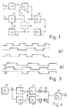
- FIG. 4 shows an embodiment in which components 30 and 31 of FIG. 1 are replaced by components 50..58.
- 50 denotes an oscillator with a stable frequency, for example a quartz oscillator.
- the oscillator signal with the frequency fN is fed to the inputs of two frequency dividers 51 and 52.
- the frequency dividers 51 and 52 have different frequency divider factors, which are chosen so that there is a first reference frequency f 1, which is below the carrier frequency, and (at the output of the frequency divider 52), a second reference frequency f 2, which is just above the reference frequency.
- the frequency divider 51 should have a frequency divider factor of 53 and the frequency divider 52 a frequency divider factor of 52.
- Reference frequencies f 1 would then be equal to 75, 5 kHz and f2 equal to 76.9 kHz result. The two reference frequencies thus form a frequency window within which the desired oscillator frequency lies.
- the two frequency dividers are each with one of the frequency sensitive Coupled phase detectors 53 and 54, which can have the same structure as the frequency detector 35 explained with reference to FIG. 2.
- the reference frequencies f 1 and f 2 are each fed to the first input of the detectors 53 and 54, at the second input of which the oscillator frequency f o is present.
- the output of the phase detector 53 is connected via the series circuit of a resistor 55 and a diode 75 to the low-pass filter 26 of the PLL circuit, which is not shown in any more detail.
- the output of the phase detector 54 is also connected to the low-pass filter 26 via the series connection of a resistor 56 and a diode 58, but the diode 58 (seen from the low-pass filter 26) is polarized in the opposite direction to the diode 57.
- the circuit according to Figure 4 works as follows when the idle frequency f o of the oscillator is below the reference frequency f 1:
- the two detectors 53 and 54 deliver current pulses with positive polarity, whereby only the current pulses supplied by the detector 53 can reach the input of the low pass 26 because the positive current pulses of the detector 54 are suppressed by the diode 58. This results in a voltage at the output of the filter which detunes the controlled oscillator 21 (not shown in FIG. 4) at higher frequencies.
- the oscillator frequency f o has reached or exceeded the value of the reference frequency f 1
- the polarity of the current pulses supplied by the detector 53 is reversed, but these are not effective because of the diode 57.
- both detectors 53 and 54 deliver current pulses with negative polarity; however, the current pulses from the detector 53 are suppressed by the diode 57.
- the negative current pulses cause the low-pass filter 26 to detune the controlled oscillator 21 in frequency towards lower frequencies until it has reached the value f 2.
- the polarity of the signals provided by detector 54 is reversed; however, these signals are now suppressed by diode 58.
- the phase detectors 53 and 54 are then both ineffective and the detuning of the controlled oscillator then takes place by means of the PLL circuit.
- the oscillator is retuned exclusively with the aid of the PLL circuit.
- the advantage of the circuit according to FIG. 4 compared to the circuit according to FIG. 2 is that the nominal value of the idle frequency of the oscillator can be identical to the frequency which the oscillator assumes in the synchronized state. Despite production variation and temperature fluctuations, the difference between the frequency of the oscillator in the synchronized state and the idling frequency is generally smaller than in the case of a circuit according to FIG. 2, so that smaller phase errors result. However, the expense for frequency divider, phase detector and blocking circuit is twice as high as for the circuit according to FIG. 2.
- FIG. 5 A circuit that has the same advantages as that The circuit according to FIG. 2 and which is less complex is shown in FIG. 5.
- the connections of the series circuit 55, 56, 58 are each connected via an AND gate 62 or 63 to the output of a frequency-sensitive phase detector 61, which can have the same structure as the detector 35 in FIG. 2; the input of this detector is connected to the output of a switchable frequency divider 60, the input of which is supplied with the stable frequency f N.
- the output of the AND gate 63 is inverted and also its input connected to the output of the detector 61.
- Pulses with positive polarity can thus reach the low-pass filter 26 via the resistance diode path 55, 57, and those with negative polarity can reach the low-pass filter 56,58 - if a suitable signal is read at the second input of the upstream AND circuit 62 and 63.
- This signal A which determines the frequency divider factor of the circuit 60, is fed directly to the second input of the AND circuit 62 and to the second input of the AND circuit 63 via an inverter 64.
- the output signal has the frequency divider circuit 60 the Wertf2. If the oscillator frequency f o is above the frequency f 2, the detector 61 delivers pulses with negative polarity, which can then reach the low-pass filter 26 via the AND gate 63 and the diode 56 and the resistor 58, the output signal of which does not show the in the voltage controllable oscillator 21 (Fig. 1) detuned until the oscillator frequency f o falls below the value f2. The output pulses then acquire a positive polarity which would be suppressed by diode 56 and which diode 55 cannot reach because AND gate 62 is blocked.
- the oscillator is detuned until the oscillator frequency is in the range between f1 and f2. The circuit then becomes ineffective.
- the circuit is also not effective.
- the signal A must be inverted. This can be done by periodically inverting the signal with a sufficiently long period.
- a logic circuit not shown in FIG. 5, which inverts the polarity of the signal A whenever there are no (positive or negative) pulses at the connection point of the resistors 57 and 58.
- PLL stereo decoder used in decoding circuits for traffic radio or the radio data system.
- PLL demodulator circuits use in PLL demodulator circuits is possible in which the oscillator is to be synchronized with a known carrier frequency.
Landscapes
- Engineering & Computer Science (AREA)
- Power Engineering (AREA)
- Stabilization Of Oscillater, Synchronisation, Frequency Synthesizers (AREA)
Applications Claiming Priority (2)
| Application Number | Priority Date | Filing Date | Title |
|---|---|---|---|
| DE3816696A DE3816696A1 (de) | 1988-05-17 | 1988-05-17 | Schaltungsanordnung zum synchronisieren eines in der frequenz steuerbaren oszillators |
| DE3816696 | 1988-05-17 |
Publications (3)
| Publication Number | Publication Date |
|---|---|
| EP0342740A2 EP0342740A2 (de) | 1989-11-23 |
| EP0342740A3 EP0342740A3 (en) | 1990-11-07 |
| EP0342740B1 true EP0342740B1 (de) | 1995-08-23 |
Family
ID=6354496
Family Applications (1)
| Application Number | Title | Priority Date | Filing Date |
|---|---|---|---|
| EP89201186A Expired - Lifetime EP0342740B1 (de) | 1988-05-17 | 1989-05-11 | Schaltungsanordnung zum Synchronisieren eines in der Frequenz steuerbaren Oszillators |
Country Status (4)
| Country | Link |
|---|---|
| US (1) | US5003272A (ja) |
| EP (1) | EP0342740B1 (ja) |
| JP (1) | JP2877834B2 (ja) |
| DE (2) | DE3816696A1 (ja) |
Families Citing this family (4)
| Publication number | Priority date | Publication date | Assignee | Title |
|---|---|---|---|---|
| DE4102562A1 (de) * | 1991-01-29 | 1992-07-30 | Thomson Brandt Gmbh | Verfahren und schaltung fuer eine automatische, hochpraezise frequenz-feinabstimmung |
| SE9801092L (sv) * | 1998-03-30 | 1999-10-01 | Telia Ab | Arrangemang och metod vid ett mobilt radiokommunikationssystem |
| EP0989676A1 (en) * | 1998-09-21 | 2000-03-29 | TRT Lucent Technologies (SA) | Frequency presetting device for a voltage controlled oscillator |
| EP0989675A1 (fr) * | 1998-09-21 | 2000-03-29 | TRT Lucent Technologies (SA) | Dispositif de prépositionnement en fréquence d'un oscillateur commandé en tension |
Family Cites Families (10)
| Publication number | Priority date | Publication date | Assignee | Title |
|---|---|---|---|---|
| US3458823A (en) * | 1967-03-20 | 1969-07-29 | Weston Instruments Inc | Frequency coincidence detector |
| US3796962A (en) * | 1972-10-06 | 1974-03-12 | Hekimian Laboratories Inc | Phase lock loop and frequency discriminator employed therein |
| US3909743A (en) * | 1974-02-25 | 1975-09-30 | Int Standard Electric Corp | Frequency synthesizer with pseudo-reference phase comparator |
| US4280104A (en) * | 1979-08-10 | 1981-07-21 | Matsushita Electric Corporation Of America | Phase locked loop system with improved acquisition |
| US4320356A (en) * | 1980-02-21 | 1982-03-16 | The United States Of America As Represented By The Secretary Of The Air Force | High speed frequency acquisition apparatus for microwave synthesizers |
| US4365211A (en) * | 1980-10-31 | 1982-12-21 | Westinghouse Electric Corp. | Phase-locked loop with initialization loop |
| US4484152A (en) * | 1982-05-19 | 1984-11-20 | Westinghouse Electric Corp. | Phase-locked loop having improved locking capabilities |
| US4590602A (en) * | 1983-08-18 | 1986-05-20 | General Signal | Wide range clock recovery circuit |
| US4580107A (en) * | 1984-06-06 | 1986-04-01 | The United States Of America As Represented By The Secretary Of The Air Force | Phase lock acquisition system having FLL for coarse tuning and PLL for fine tuning |
| US4787097A (en) * | 1987-02-11 | 1988-11-22 | International Business Machines Corporation | NRZ phase-locked loop circuit with associated monitor and recovery circuitry |
-
1988
- 1988-05-17 DE DE3816696A patent/DE3816696A1/de not_active Withdrawn
-
1989
- 1989-05-11 DE DE58909391T patent/DE58909391D1/de not_active Expired - Fee Related
- 1989-05-11 EP EP89201186A patent/EP0342740B1/de not_active Expired - Lifetime
- 1989-05-16 US US07/352,446 patent/US5003272A/en not_active Expired - Fee Related
- 1989-05-17 JP JP1124110A patent/JP2877834B2/ja not_active Expired - Lifetime
Also Published As
| Publication number | Publication date |
|---|---|
| EP0342740A3 (en) | 1990-11-07 |
| DE58909391D1 (de) | 1995-09-28 |
| JP2877834B2 (ja) | 1999-04-05 |
| DE3816696A1 (de) | 1989-11-30 |
| US5003272A (en) | 1991-03-26 |
| JPH02111123A (ja) | 1990-04-24 |
| EP0342740A2 (de) | 1989-11-23 |
Similar Documents
| Publication | Publication Date | Title |
|---|---|---|
| DE69424373T2 (de) | Phasenregelschleife mit Überbrückungsmodus | |
| DE4498749C2 (de) | Phasensynchronisationsschaltung und entsprechendes Verfahren für einen phasenverriegelten Kreis | |
| DE3424786A1 (de) | Mehrfrequenz-mikrowellensignalquelle | |
| DE3880391T2 (de) | Verbesserte phasenregelschleife. | |
| DE2744432A1 (de) | Phasen- oder frequenzsteuerkreis im rueckkopplungskreis des oszillators eines fernseh-kanalwaehlers o.dgl. | |
| DE69300291T2 (de) | Frequenzregelschleife. | |
| DE68927158T2 (de) | PLL-Synthetisierer | |
| DE3123973C2 (de) | Phasenregelschaltung | |
| DE2836724A1 (de) | Schaltungsanordnung zur bestimmung von zeitintervallen | |
| DE2848881C2 (ja) | ||
| DE69302442T2 (de) | Phasenregelkreis mit zwei Betriebsorten | |
| DE3321601A1 (de) | Steuerschaltung fuer eine phasenstarre schleife | |
| DE2603641A1 (de) | Phasenstarre rueckfuehrschleife, insbesondere fuer einen breitbandsender | |
| EP0141452A2 (de) | Schaltungsanordnung für einen Empfänger mit zwei Phasenregelkreisen | |
| EP0342740B1 (de) | Schaltungsanordnung zum Synchronisieren eines in der Frequenz steuerbaren Oszillators | |
| DE4220228B4 (de) | Schaltungsanordnung zur Unterdrückung schmalbandiger Störsignale | |
| DE3046540A1 (de) | Phasenregelkreis | |
| DE2944258A1 (de) | Automatischer feinabstimmkreis | |
| DE60114733T2 (de) | Phasenregelschleife mit verringerter Verriegelungszeit | |
| EP0544355B1 (de) | Digitaler Phasenregelkreis | |
| DE2741697C2 (ja) | ||
| DE4220296B4 (de) | Schaltungsanordnung zur Unterdrückung schmalbandiger Störsignale | |
| DE2802626C2 (de) | Digitale Phasenvergleichsanordnung | |
| DE69213351T2 (de) | Empfänger mit einer Phasenregelschleife | |
| DE2641501C3 (de) | Abstimmbarer Oszillator hoher Frequenzgenauigkeit und Konstanz |
Legal Events
| Date | Code | Title | Description |
|---|---|---|---|
| PUAI | Public reference made under article 153(3) epc to a published international application that has entered the european phase |
Free format text: ORIGINAL CODE: 0009012 |
|
| AK | Designated contracting states |
Kind code of ref document: A2 Designated state(s): DE FR GB |
|
| PUAL | Search report despatched |
Free format text: ORIGINAL CODE: 0009013 |
|
| AK | Designated contracting states |
Kind code of ref document: A3 Designated state(s): DE FR GB |
|
| 17P | Request for examination filed |
Effective date: 19910502 |
|
| 17Q | First examination report despatched |
Effective date: 19930922 |
|
| GRAA | (expected) grant |
Free format text: ORIGINAL CODE: 0009210 |
|
| AK | Designated contracting states |
Kind code of ref document: B1 Designated state(s): DE FR GB |
|
| REF | Corresponds to: |
Ref document number: 58909391 Country of ref document: DE Date of ref document: 19950928 |
|
| GBT | Gb: translation of ep patent filed (gb section 77(6)(a)/1977) |
Effective date: 19951115 |
|
| ET | Fr: translation filed | ||
| PLBE | No opposition filed within time limit |
Free format text: ORIGINAL CODE: 0009261 |
|
| STAA | Information on the status of an ep patent application or granted ep patent |
Free format text: STATUS: NO OPPOSITION FILED WITHIN TIME LIMIT |
|
| 26N | No opposition filed | ||
| PGFP | Annual fee paid to national office [announced via postgrant information from national office to epo] |
Ref country code: GB Payment date: 19980501 Year of fee payment: 10 |
|
| PGFP | Annual fee paid to national office [announced via postgrant information from national office to epo] |
Ref country code: FR Payment date: 19980519 Year of fee payment: 10 |
|
| REG | Reference to a national code |
Ref country code: FR Ref legal event code: CD |
|
| PG25 | Lapsed in a contracting state [announced via postgrant information from national office to epo] |
Ref country code: GB Free format text: LAPSE BECAUSE OF NON-PAYMENT OF DUE FEES Effective date: 19990511 |
|
| GBPC | Gb: european patent ceased through non-payment of renewal fee |
Effective date: 19990511 |
|
| PG25 | Lapsed in a contracting state [announced via postgrant information from national office to epo] |
Ref country code: FR Free format text: LAPSE BECAUSE OF NON-PAYMENT OF DUE FEES Effective date: 20000131 |
|
| REG | Reference to a national code |
Ref country code: FR Ref legal event code: ST |
|
| PGFP | Annual fee paid to national office [announced via postgrant information from national office to epo] |
Ref country code: DE Payment date: 20010717 Year of fee payment: 13 |
|
| PG25 | Lapsed in a contracting state [announced via postgrant information from national office to epo] |
Ref country code: DE Free format text: LAPSE BECAUSE OF NON-PAYMENT OF DUE FEES Effective date: 20021203 |