EP0341708B1 - Résistance en couche mince et procédé de fabrication - Google Patents
Résistance en couche mince et procédé de fabrication Download PDFInfo
- Publication number
- EP0341708B1 EP0341708B1 EP89108477A EP89108477A EP0341708B1 EP 0341708 B1 EP0341708 B1 EP 0341708B1 EP 89108477 A EP89108477 A EP 89108477A EP 89108477 A EP89108477 A EP 89108477A EP 0341708 B1 EP0341708 B1 EP 0341708B1
- Authority
- EP
- European Patent Office
- Prior art keywords
- complexes
- rhodium
- organometallic material
- atoms
- substrate
- Prior art date
- Legal status (The legal status is an assumption and is not a legal conclusion. Google has not performed a legal analysis and makes no representation as to the accuracy of the status listed.)
- Expired - Lifetime
Links
Images
Classifications
-
- H—ELECTRICITY
- H01—ELECTRIC ELEMENTS
- H01C—RESISTORS
- H01C17/00—Apparatus or processes specially adapted for manufacturing resistors
-
- H—ELECTRICITY
- H01—ELECTRIC ELEMENTS
- H01C—RESISTORS
- H01C7/00—Non-adjustable resistors formed as one or more layers or coatings; Non-adjustable resistors made from powdered conducting material or powdered semi-conducting material with or without insulating material
- H01C7/006—Thin film resistors
-
- H—ELECTRICITY
- H01—ELECTRIC ELEMENTS
- H01C—RESISTORS
- H01C17/00—Apparatus or processes specially adapted for manufacturing resistors
- H01C17/06—Apparatus or processes specially adapted for manufacturing resistors adapted for coating resistive material on a base
- H01C17/075—Apparatus or processes specially adapted for manufacturing resistors adapted for coating resistive material on a base by thin-film techniques
-
- H—ELECTRICITY
- H01—ELECTRIC ELEMENTS
- H01C—RESISTORS
- H01C17/00—Apparatus or processes specially adapted for manufacturing resistors
- H01C17/06—Apparatus or processes specially adapted for manufacturing resistors adapted for coating resistive material on a base
- H01C17/20—Apparatus or processes specially adapted for manufacturing resistors adapted for coating resistive material on a base by pyrolytic processes
-
- H—ELECTRICITY
- H01—ELECTRIC ELEMENTS
- H01C—RESISTORS
- H01C7/00—Non-adjustable resistors formed as one or more layers or coatings; Non-adjustable resistors made from powdered conducting material or powdered semi-conducting material with or without insulating material
- H01C7/003—Thick film resistors
Definitions
- the present invention relates to a resistor for use in hydrid ICs and various other electronic devices and a process for producing the resistor. Specifically, the invention relates to a thin-film uniform resistor and a process for producing the same.
- resistors useful in electronic devices such as hybrid ICs and thermal heads.
- One method is a thick-film process in which a coating of thick-film resistor paste is formed on a substrate which is then fired to make a resistor, and the other method is a thin-film process employing sputtering or other thin-film depositing techniques.
- a powder mixture of ruthenium oxide and glass frit is dispersed in an organic vehicle made of a solvent and a resin, and the resulting thick-film resistor paste is screen-printed on a substrate, which is then fired to make a resistor.
- a thin film of a refractory metal such as tantalum is deposited on a substrate by sputtering, and a patterned thin-film resistor is fabricated by photolithographic techniques. This method is used to fabricate some of the thermal heads in current use.
- the conventional thick-film process which uses thick-film resistor paste has the advantage of achieving high production rate with inexpensive facilities.
- the resistors produced by this process have the problem of low stability to an electic field, i.e. their resistance changes sharply when they are subjected to voltage variations.
- the thick-film process has the following additional disadvantages; the resistance value of the final product cannot be effectively controlled by adjusting the proportions of glass frit and ruthenium oxide alone, also great variations in resistance will occur, not only because of the difference in the particle sizes of glass frit and ruthenium oxide powder, but also, upon the firing temperature used. Even if the same compositional range and average particle size are used, the value of resistance will differ from one lot to another.
- the thin-film process is capable of producing uniform thin-film resistors but, on the other hand, this method requires expensive facilities, and achieves only a low production rate.
- the document DE-A 1,490,606 discloses an electrical resistor comprising several layers on a substrate of glas, ceramic material etc., wherein the electrically restistive layers comprise gold, platinum, palladium and rhodium or rhodium oxide.
- the ratio of metals other than rhodium to rhodium is in the range of 9.0 to 19 and hence, exceeds the present range considerably.
- the document US-A 3,681,261 is concerned with a resistor composition wherein the resistive metal may, inter alia, be rhodium, and wherein other metals are employed as metal stabilizers which metal stabilizers are selected from the group consisting of silver, gold, platinum and mixtures thereof. Furthermore, so-called "anti-agglomerating agents" are added to the composition from which the resistor is formed. Said anti-agglomerating agents are added in order to prevent agglomeration of the resistive metal and metal stabilizer during alloying thereof. Such anti-agglomerating agents may comprise aluminum oxide or titanium oxide.
- FR-A 2,192,361 discloses composable masses for the preparation of electric resistors wherein organometallic compounds of Bi, Si, B, Al, Pb and/or Ti are employed together with a nobel metal such as, for example, rhodium.
- a nobel metal such as, for example, rhodium.
- the nonenoble metal materials are employed for the purpose of TCR adjustment.
- the thin-film resistor, and the method of production of the same resistor, in accordance with the present invention will provide the following advantages over that of known film resistors. It is to be understood that this list is exemplary in nature and the advantages are not limited to what is listed herein.
- a thin-film resistor comprising a mixture of rhodium (Rh) oxide as a resistive material, and at least one element (M) selected from the group consisting of silicon (Si), lead (Pb), bismuth (Bi), zirconium (Zr), barium (Ba), aluminium (Al), boron (B), tin (Sn), and titanium (Ti), wherein the ratio of the number of element (M) atoms to that of rhodium (Rh) atoms, M/Rh, is in the range of 0.3 - 3.0.
- This thin-film resistor is formed from the process of preparing a solution of an organometallic material containing rhodium (Rh), and at least one element (M) selected from the group consisting of silicon (Si), lead (Pb), bismuth (Bi), zirconium (Zr), barium (Ba), aluminum (Al), boron (B), tin (Sn), and titanium (Ti), wherein the ratio of the number of element (M) atoms to that of rhodium (Rh) atoms, M/Rh, is in the range of 0.3 to 3.0; adjusting the viscosity of the solution to 5,000 - 30,000 cPs; coating the organometallic material on a substrate, drying of the organometallic material coated on the substrate; and firing, in air, the organometallic material coated on the substrate at a peak temperature not lower than 500°C.
- element (M) selected from the group consisting of silicon (Si), lead (Pb), bismuth (
- a thin-film resistor that contains rhodium oxide as a resistive material and at least one other metal selected as described above.
- this thin-film resistor is formed as follows: A solution of an organometallic material containing as resistive materials, not only rhodium (Rh), but also, at least one metal (M) selected from the group consisting of silicon (Si), aluminium (Al), barium (Ba), tin (Sn), titanium (Ti), zirconium (Zr), boron (B), lead (Pb) and bismuth (Bi) in such amounts that M/Rh, or the ratio of the number of metal atoms to that of rhodium atoms, is in the range of 0.3 to 3.0.
- the resulting organometallic material solution is then coated onto a substrate followed by the drying of that organometallic material solution.
- the solution coated substrate is then fired in air at a peak temperature not lower than 500°C.
- the resulting resistor contains rhodium oxide (RhO2), with the other metals forming a homogeneous structure in the form of their oxides or ternary oxides of them and rhodium.
- RhO2 rhodium oxide
- Metal Resinate (trade name of Engelhard Minerals & Chemicals Corporation) of the following identification numbers were used as solutions of organometallic material: Rh ... # 8826 Si ... # 28-FC Al ... # A-3808 Ba ... # 137-C Sn ... # 118-B Ti ... # 9428 Zr ... # 54237 B ... # 11-A Pb ... # 207-A Bi ... # 8365
- the sheet resistances of some of the resistors fabricated in the example under consideration are shown in Table 1.
- the data in Table 1 refers to the films that were prepared using as a vehicle a mixture composed of 70 wt% solvent and 30 wt% resin; printing was done with a screen of 200 mesh and subsequent firing was conducted at a peak temperature of 800°C.
- organometallic materials suitable for various types of "Metal Resinate” available from Engelhard Minerals & Chemicals Corporation.
- organometallic materials can be prepared from complexes of rhodium or other metals, such as Si, Bi, and Pb, with an organic material such as carboxylic acids, which are soluble in organic solvents such as ⁇ -terpineol and butylcarbitol acetate. Suitable metal complexes are listed below.
- rhodium complexes the following preferred complexes with carboxylic acids, cyclic terpene mercaptides, ⁇ -diketones, etc. may be used: As Si complexes, and low-molecular weight silicone resins and silicon alkoxides may preferably be used.
- As Bi complex there may preferably be used: As Pb complex, there may preferably be used: As complexes of other metals, carboxylic acid complexes and metal alkoxides ( ⁇ R-O) ⁇ n M may be used.
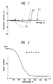
- Curve (II) represents a conventional ruthenium oxide based heating film resistor. All three were subjected to strength measurements by a step stress test (SST). The results are shown in Fig. 1, in which the horizontal axis plots power wattage (W) and the vertical axis resistance variance (%).
- the coated substrate is fired at a peak temperature of not lower than 500°C. If the firing temperature is below 500°C, greater difficulty is involved in forming a desired resistor film. This is evident from the results of thermogravimetric analysis of resistor film shown in Fig. 2 for a resinate having a Rh:Si:Bi value of 1:0.5:0.5. At 500°C and above, the weight of the film remained practically constant, suggesting the completion of film formation for heating resistor.
Landscapes
- Engineering & Computer Science (AREA)
- Microelectronics & Electronic Packaging (AREA)
- Manufacturing & Machinery (AREA)
- Physics & Mathematics (AREA)
- Electromagnetism (AREA)
- Apparatuses And Processes For Manufacturing Resistors (AREA)
- Non-Adjustable Resistors (AREA)
- Electronic Switches (AREA)
- Conductive Materials (AREA)
Claims (7)
- Résistance à film mince comprenant un mélange d'oxyde de rhodium (Rh) comme matériau résistant, et au moins un élément (M) choisi dans le groupe comprenant le silicium (Si), le plomb (Pb), le bismuth (Bi), le zirconium (Zr), le baryum (Ba), l'aluminium (Al), le bore (B), l'étain (Sn) et le titane (Ti) dans lequel le rapport du nombre d'atomes de l'élément (M) à celui des atomes de rhodium (Rh), soit M/Rh, est compris dans l'intervalle 0,3 - 3,0.
- Résistance à film mince selon la revendication 1, dans laquelle le mélange comprend :- comme complexes du rhodium
 - comme complexes de Si
 - comme complexes de Bi
 - comme complexes de Pb
- Procédé pour former une résistance à film mince comprenant un mélange d'oxyde de rhodium (Rh) comme matériau résistant, et au moins un élément (M) choisi dans le groupe comprenant le silicium (Si), le plomb (Pb), le bismuth (Bi), le zirconium (Zr), le baryum (Ba), l'aluminium (Al), le bore (B), l'étain (Sn) et le titane (Ti), dans lequel le rapport du nombre d'atomes de l'élément (M) à celui des atomes de rhodium (Rh), soit M/Rh, est compris dans l'intervalle 0,3 - 3,0, qui comprend les étapes consistant :- à préparer une solution d'un matériau organométallique contenant du rhodium (Rh) et au moins un élément (M) choisi dans le groupe comprenant le silicium (Si), le plomb (Pb), le bismuth (Bi), le zirconium (Zr), le baryum (Ba), l'aluminium (Al), le bore (B) l'étain (Sn) et le titane (Ti), dans lequel le rapport du nombre d'atomes de l'élément (M) à celui des atomes de rhodium (Rh), soit M/Rh, est compris dans l'intervalle 0,3 - 3,0 ;- à ajuster la viscosité de cette solution d'un matériau organométallique à 5.000-30.000 cP ;- à appliquer ce matériau organométallique sur un substrat ;- à sécher le matériau organométallique appliqué sur le susbtrat ; et- à cuire, dans l'air, le matériau organométallique appliqué sur le substrat, à une température maximale non inférieure à 500°C.
- Procédé selon la revendication 3, dans lequel l'étape de séchage de la solution d'un matériau organométallique appliqué sur le substrat est effectuée à une température d'environ 120 °C.
- Procédé selon la revendication 3 ou 4, dans lequel l'étape de cuisson du matériau organométallique appliqué sur le substrat dure environ 10 minutes.
- Procédé selon l'une quelconque des revendications 3 à 5, dans lequel l'étape de cuisson du matériau organométallique appliqué sur le substrat s'effectue à une température comprise entre 500 et 800 °C.
- Procédé selon l'une quelconque des revendications 3 à 6, dans lequel la solution du matériau organométallique comprend :- comme complexes du rhodium
 - comme complexes de Si
 - comme complexes de Bi
 - comme complexes de Pb
Applications Claiming Priority (2)
| Application Number | Priority Date | Filing Date | Title |
|---|---|---|---|
| JP63116444A JPH07105282B2 (ja) | 1988-05-13 | 1988-05-13 | 抵抗体及び抵抗体の製造方法 |
| JP116444/88 | 1988-05-13 |
Publications (3)
| Publication Number | Publication Date |
|---|---|
| EP0341708A2 EP0341708A2 (fr) | 1989-11-15 |
| EP0341708A3 EP0341708A3 (en) | 1990-11-22 |
| EP0341708B1 true EP0341708B1 (fr) | 1994-04-27 |
Family
ID=14687264
Family Applications (1)
| Application Number | Title | Priority Date | Filing Date |
|---|---|---|---|
| EP89108477A Expired - Lifetime EP0341708B1 (fr) | 1988-05-13 | 1989-05-11 | Résistance en couche mince et procédé de fabrication |
Country Status (5)
| Country | Link |
|---|---|
| US (1) | US5633035A (fr) |
| EP (1) | EP0341708B1 (fr) |
| JP (1) | JPH07105282B2 (fr) |
| KR (1) | KR0123907B1 (fr) |
| DE (1) | DE68914876T2 (fr) |
Families Citing this family (7)
| Publication number | Priority date | Publication date | Assignee | Title |
|---|---|---|---|---|
| US5510823A (en) * | 1991-03-07 | 1996-04-23 | Fuji Xerox Co., Ltd. | Paste for resistive element film |
| JPH04279003A (ja) * | 1991-03-07 | 1992-10-05 | Fuji Xerox Co Ltd | 抵抗体膜形成用ペースト |
| AUPP599598A0 (en) * | 1998-09-18 | 1998-10-08 | Email Limited | Self-regulating nanoscale heating element |
| RU2170474C2 (ru) * | 1998-11-23 | 2001-07-10 | АООТ "НИИ молекулярной электроники и завод "Микрон" | Способ изготовления резисторов в интегральных схемах |
| JP3935687B2 (ja) * | 2001-06-20 | 2007-06-27 | アルプス電気株式会社 | 薄膜抵抗素子およびその製造方法 |
| TW200612443A (en) * | 2004-09-01 | 2006-04-16 | Tdk Corp | Thick-film resistor paste and thick-film resistor |
| JP2025519767A (ja) | 2022-11-05 | 2025-06-26 | バンアム インク. | 酸化物薄膜 |
Family Cites Families (26)
| Publication number | Priority date | Publication date | Assignee | Title |
|---|---|---|---|---|
| NL83230C (fr) * | 1950-01-25 | |||
| DE1490606A1 (de) * | 1964-07-09 | 1970-07-16 | Siemens Ag | Elektrischer Schichtwiderstand mit geringem Temperaturbeiwert des elektrischen Widerstandes |
| USRE28820E (en) * | 1965-05-12 | 1976-05-18 | Chemnor Corporation | Method of making an electrode having a coating containing a platinum metal oxide thereon |
| GB1195833A (en) * | 1966-06-14 | 1970-06-24 | Plessey Co Ltd | Improvements in or relating to Resistors |
| US3619287A (en) * | 1968-09-20 | 1971-11-09 | Carrier Corp | Process of producing an electrical resistor |
| US3620840A (en) * | 1968-12-13 | 1971-11-16 | Methode Dev Co | Resistance material and resistance elements made therefrom |
| US3673117A (en) * | 1969-12-19 | 1972-06-27 | Methode Dev Co | Electrical resistant material |
| US3681261A (en) * | 1970-07-27 | 1972-08-01 | Owens Illinois Inc | Resistors,compositions,pastes,and method of making and using same |
| US3809797A (en) * | 1971-11-16 | 1974-05-07 | Du Pont | Seal ring compositions and electronic packages made therewith |
| DE2233654A1 (de) * | 1972-07-08 | 1974-01-24 | Degussa | Thermisch zersetzbare masse zur herstellung von elektrischen widerstaenden |
| JPS5477286A (en) * | 1977-12-02 | 1979-06-20 | Tdk Corp | Manufacture of insoluble electrode |
| SU714508A1 (ru) * | 1977-12-06 | 1980-02-05 | Предприятие П/Я В-8574 | Токопровод ща композици |
| US4330331A (en) * | 1978-06-16 | 1982-05-18 | Nippon Telegraph And Telephone Public Corporation | Electric contact material and method of producing the same |
| US4302362A (en) * | 1979-01-23 | 1981-11-24 | E. I. Du Pont De Nemours And Company | Stable pyrochlore resistor compositions |
| JPS5727506A (en) * | 1980-07-25 | 1982-02-13 | Central Glass Co Ltd | Conductive paste |
| US4415624A (en) * | 1981-07-06 | 1983-11-15 | Rca Corporation | Air-fireable thick film inks |
| US4362656A (en) * | 1981-07-24 | 1982-12-07 | E. I. Du Pont De Nemours And Company | Thick film resistor compositions |
| US4476039A (en) * | 1983-01-21 | 1984-10-09 | E. I. Du Pont De Nemours And Company | Stain-resistant ruthenium oxide-based resistors |
| CA1217927A (fr) * | 1983-04-15 | 1987-02-17 | Tsutomu Nanao | Materiau composite inorganique, et sa preparation |
| DE3479053D1 (en) * | 1983-10-28 | 1989-08-24 | Ngk Spark Plug Co | Gas sensor with ceramics substrate and method for producing the same |
| JPS60101701A (ja) * | 1983-11-08 | 1985-06-05 | Matsushita Electric Ind Co Ltd | 針圧制御回路 |
| JPS60102701A (ja) * | 1983-11-10 | 1985-06-06 | アルプス電気株式会社 | 厚膜抵抗層形成用ペ−スト |
| JPS60130494A (ja) * | 1983-12-16 | 1985-07-11 | Kitsudo:Kk | ダイボンディング用導電性ペ−スト |
| US4539223A (en) * | 1984-12-19 | 1985-09-03 | E. I. Du Pont De Nemours And Company | Thick film resistor compositions |
| JP2699381B2 (ja) * | 1987-04-28 | 1998-01-19 | 富士ゼロックス株式会社 | 抵抗体の製造方法 |
| JP2617110B2 (ja) * | 1988-02-29 | 1997-06-04 | 富士ゼロックス株式会社 | 抵抗体の製造方法 |
-
1988
- 1988-05-13 JP JP63116444A patent/JPH07105282B2/ja not_active Expired - Fee Related
-
1989
- 1989-05-10 KR KR1019890006238A patent/KR0123907B1/ko not_active Expired - Fee Related
- 1989-05-11 EP EP89108477A patent/EP0341708B1/fr not_active Expired - Lifetime
- 1989-05-11 DE DE68914876T patent/DE68914876T2/de not_active Expired - Fee Related
-
1995
- 1995-04-25 US US08/428,835 patent/US5633035A/en not_active Expired - Fee Related
Also Published As
| Publication number | Publication date |
|---|---|
| KR890017727A (ko) | 1989-12-18 |
| DE68914876T2 (de) | 1994-12-08 |
| KR0123907B1 (ko) | 1997-12-09 |
| JPH01286402A (ja) | 1989-11-17 |
| JPH07105282B2 (ja) | 1995-11-13 |
| EP0341708A3 (en) | 1990-11-22 |
| EP0341708A2 (fr) | 1989-11-15 |
| DE68914876D1 (de) | 1994-06-01 |
| US5633035A (en) | 1997-05-27 |
Similar Documents
| Publication | Publication Date | Title |
|---|---|---|
| JP3907725B2 (ja) | カドミウムおよび鉛を含有しない厚膜ペースト組成物 | |
| US4362656A (en) | Thick film resistor compositions | |
| DE69017804T2 (de) | Thermistorzusammensetzung. | |
| EP0115798B1 (fr) | Résistances à base d'oxyde de ruthénium, résistant à la tacheture | |
| US3682840A (en) | Electrical resistor containing lead ruthenate | |
| US4209764A (en) | Resistor material, resistor made therefrom and method of making the same | |
| JP2617110B2 (ja) | 抵抗体の製造方法 | |
| JPS61145805A (ja) | 厚膜抵抗体組成物 | |
| DE3026021A1 (de) | Dickfilmwiderstandspaste und daraus hergestellte widerstaende | |
| DE2551036B2 (de) | Borid-stoffzusammensetzung und ihre verwendung | |
| US5633035A (en) | Thin-film resistor and process for producing the same | |
| US4076894A (en) | Electrical circuit element comprising thick film resistor bonded to conductor | |
| US5463367A (en) | Method for forming thick film resistors and compositions therefor | |
| US5053249A (en) | Method for producing resistors | |
| JPH05234703A (ja) | 厚膜抵抗体を製造するための抵抗組成物 | |
| US3951672A (en) | Glass frit containing lead ruthenate or lead iridate in relatively uniform dispersion and method to produce same | |
| JPH0450721B2 (fr) | ||
| JP3253121B2 (ja) | 厚膜抵抗体組成物 | |
| EP0432353B1 (fr) | Masse résistive et son utilisation | |
| JP2759995B2 (ja) | 抵抗体の製造方法及びその抵抗体を用いたサーマルヘッドの製造方法 | |
| JP2526431B2 (ja) | 抵抗体およびその製造方法 | |
| JPH113802A (ja) | 低温焼成用抵抗ペースト | |
| JPH01304702A (ja) | 抵抗体の製造方法及びサーマルヘッドの製造方法 | |
| JP3094683B2 (ja) | 厚膜抵抗体形成用組成物 | |
| JP2817151B2 (ja) | 抵抗体の製造方法及びサーマルヘッドの製造方法 |
Legal Events
| Date | Code | Title | Description |
|---|---|---|---|
| PUAI | Public reference made under article 153(3) epc to a published international application that has entered the european phase |
Free format text: ORIGINAL CODE: 0009012 |
|
| AK | Designated contracting states |
Kind code of ref document: A2 Designated state(s): DE GB |
|
| PUAL | Search report despatched |
Free format text: ORIGINAL CODE: 0009013 |
|
| AK | Designated contracting states |
Kind code of ref document: A3 Designated state(s): DE GB |
|
| 17P | Request for examination filed |
Effective date: 19901213 |
|
| 17Q | First examination report despatched |
Effective date: 19921006 |
|
| GRAA | (expected) grant |
Free format text: ORIGINAL CODE: 0009210 |
|
| AK | Designated contracting states |
Kind code of ref document: B1 Designated state(s): DE GB |
|
| REF | Corresponds to: |
Ref document number: 68914876 Country of ref document: DE Date of ref document: 19940601 |
|
| PLBE | No opposition filed within time limit |
Free format text: ORIGINAL CODE: 0009261 |
|
| STAA | Information on the status of an ep patent application or granted ep patent |
Free format text: STATUS: NO OPPOSITION FILED WITHIN TIME LIMIT |
|
| 26N | No opposition filed | ||
| REG | Reference to a national code |
Ref country code: GB Ref legal event code: IF02 |
|
| PGFP | Annual fee paid to national office [announced via postgrant information from national office to epo] |
Ref country code: GB Payment date: 20030507 Year of fee payment: 15 |
|
| PGFP | Annual fee paid to national office [announced via postgrant information from national office to epo] |
Ref country code: DE Payment date: 20030522 Year of fee payment: 15 |
|
| PG25 | Lapsed in a contracting state [announced via postgrant information from national office to epo] |
Ref country code: GB Free format text: LAPSE BECAUSE OF NON-PAYMENT OF DUE FEES Effective date: 20040511 |
|
| PG25 | Lapsed in a contracting state [announced via postgrant information from national office to epo] |
Ref country code: DE Free format text: LAPSE BECAUSE OF NON-PAYMENT OF DUE FEES Effective date: 20041201 |
|
| GBPC | Gb: european patent ceased through non-payment of renewal fee |
Effective date: 20040511 |