EP0338480B1 - Procédé pour remplir des tranchées à partir d'une couche de germination - Google Patents
Procédé pour remplir des tranchées à partir d'une couche de germination Download PDFInfo
- Publication number
- EP0338480B1 EP0338480B1 EP89106844A EP89106844A EP0338480B1 EP 0338480 B1 EP0338480 B1 EP 0338480B1 EP 89106844 A EP89106844 A EP 89106844A EP 89106844 A EP89106844 A EP 89106844A EP 0338480 B1 EP0338480 B1 EP 0338480B1
- Authority
- EP
- European Patent Office
- Prior art keywords
- trench
- seed layer
- layer
- dielectric
- sidewall
- Prior art date
- Legal status (The legal status is an assumption and is not a legal conclusion. Google has not performed a legal analysis and makes no representation as to the accuracy of the status listed.)
- Expired - Lifetime
Links
Images


Classifications
-
- H—ELECTRICITY
- H10—SEMICONDUCTOR DEVICES; ELECTRIC SOLID-STATE DEVICES NOT OTHERWISE PROVIDED FOR
- H10W—GENERIC PACKAGES, INTERCONNECTIONS, CONNECTORS OR OTHER CONSTRUCTIONAL DETAILS OF DEVICES COVERED BY CLASS H10
- H10W10/00—Isolation regions in semiconductor bodies between components of integrated devices
- H10W10/01—Manufacture or treatment
- H10W10/041—Manufacture or treatment of isolation regions comprising polycrystalline semiconductor materials
-
- H—ELECTRICITY
- H10—SEMICONDUCTOR DEVICES; ELECTRIC SOLID-STATE DEVICES NOT OTHERWISE PROVIDED FOR
- H10W—GENERIC PACKAGES, INTERCONNECTIONS, CONNECTORS OR OTHER CONSTRUCTIONAL DETAILS OF DEVICES COVERED BY CLASS H10
- H10W10/00—Isolation regions in semiconductor bodies between components of integrated devices
- H10W10/40—Isolation regions comprising polycrystalline semiconductor materials
Definitions
- the present invention concerns a method for forming filled trenches in electrical devices and, more particularly, an improved method for filling trenches in semiconductor or other substrates using a nucleating seed layer.
- the filled trenches may be used for isolation purposes or as capacitors or for other functions.
- trenches in semiconductor substrates and then refill the trenches with a variety of materials in order to provide isolation walls between devices in integrated circuits (IC's), or to provide buried capacitors for memory devices or other electrical functions, or for other purposes.
- Silicon is the most commonly used semiconductor substrate, but other semiconductor materials may also have trenches formed therein.
- the trenches may be filled with insulators such as silicon oxide or nitride or glasses or polymers or combinations thereof, or may be wholly or partially filled with conductors such as polycrystalline semiconductors (e.g., polysilicon or poly-germanium or mixtures thereof), or may be filled with a combination of dielectrics and conductors, as for example, with a dielectric liner and a polycrystalline semiconductor core.
- filled trenches are formed by etching a trench in a semiconductor substrate, providing a dielectric liner in the trench, applying a nucleating seed layer to the bottom of the trench or to the bottom and sides of the trench and the dielectric surface outside the trench, selectively growing a silicon layer on the seed layer to over-fill the trench, applying a planarizing layer and then etching back the planarizing layer and excess silicon to approximately the level of the substrate surface.
- Japanese patent application No. JP-A-57211747 discloses a process for filling a trench of a semiconductor device using a polycrystalline silicon seed The process includes forming a trench in a silicon substrate and growing on the substrate surface in sequence, a silicon dioxide film, a polycrystalline silicon film and a silicon nitride film. The polycrystalline silicon film is etched to provide a polycrystalline silicon film on the bottom of the trench. This remaining polycrystalline silicon film is the seed from which the polycrystalline silicon is grown to fill the trench.
- poly or the words “polylayer” and “poly layer” are intended to refer generally to polycrystalline or amorphous materials, including but not limited to semiconductor materials.
- a process for forming isolation walls for electronic devices in a substrate comprising:
- the trenches are filled with polycrystalline semiconductor.
- the process comprises providing a substrate (e.g., silicon), etching a trench therein, lining the trench with a first non-nucleating material (e.g., silicon oxide); covering the first material with a nucleating seed layer (e.g., polysilicon), and thereafter removing the seed layer from the first material on the sidewalls in an upper part of the trench leaving a second part of the seed layer on at least the bottom and optionally the sidewalls in a lower part of the trench, and filling the trench to the desired level by selectively growing additional material (e.g., polysilicon) on the seed layer.
- a substrate e.g., silicon
- a first non-nucleating material e.g., silicon oxide
- a nucleating seed layer e.g., polysilicon
- the location of the seed layer in the trench is conveniently determined by first covering the seed layer with a mask, preferably of a planarizing type material such as a resist or the like which fills the trench and extends above the substrate surface, then etching or dissolving away the portion of the mask that extends above the substrate above the seed layer in an upper part of the trench. This leaves a remaining portion of the mask in a lower part of the trench covering a lower part of the seed layer. The portion of the seed layer exposed where the mask has been removed is then etched away leaving behind the seed layer in the lower portion of the trench. The height of the seed layer on the sidewalls of the trench is easily adjusted according to how much of the mask in the trench is removed.
- a mask preferably of a planarizing type material such as a resist or the like which fills the trench and extends above the substrate surface
- the invented process has the advantage compared to the prior art that control of the fill process is simplified by providing through the etch-back of the seed layer mask, a continuously adjustable seed layer which permits improved refill without need for overfilling and etching back the refill material itself, although that is not precluded.
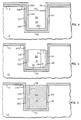
- FIGS. 1-7 show simplified schematic cross-sections through a semiconductor substrate in which a trench is formed and filled according to the present invention and at different stages in the process.
- FIG. 1 shows a portion of semiconductor substrate 10 (e.g., silicon) having surface 12 which has been covered by mask 14 having opening 16.
- Mask 14 is of any convenient material (e.g., resist or oxide or nitride or combinations therefor) for protecting surface 12 of substrate 10 from etching except in opening 16. Positive resist is convenient.
- Trench 18 having bottom 20 and sidewall 22 is etched in substrate 10 from surface 12.
- Trench 18 has depth 19 and width 21. While trench 18 is shown as having substantially vertical sidewalls, this is merely for simplicity of explanation, and not essential. In practice, it is generally desired to etch trench 18 anisotropically so that width 21 is the same or narrower than opening 16 so as to maintain good dimensional control. In general, it is desirable that trench 18 be wider at the top at surface 12 than at bottom 20. Accordingly, in most cases trench 18 will taper inwardly by a few degrees from surface 12 toward bottom 20, but this is not essential.
- resist or oxide or nitride or combinations therefor for protecting surface 12 of substrate 10
- Trench 18 usefully has depth 19 in the range of about 15 to 25 micrometers with about 20 micrometers being typical, and width 21 in the range of about 3 to 6 micrometers with about 4 micrometers being typical. However, larger or smaller values may also be used.
- Mask 14 may be removed or may be left in place. In order to leave mask 14 in place, it should be fabricated from a refractory material, such as for example, an oxide, nitride, glass or combination thereof.
- Trench 18 is covered by liner 24 (see FIG. 2). It is essential that liner 24 be substantially non-nucleating so far as the trench filling material to be applied later is concerned.
- Silicon oxide and nitride are examples of materials which may be nucleating or non-nucleating to polysilicon and other materials suitable for filling trench 18, according to the deposition conditions used with the filling materials. Deposition conditions for achieving non-nucleating behavior are well known in the art. For example, U. S. Patent 4,473,598 to Ephrath, which disclosure is incorporated herein by reference, describes procedures for depositing silicon selectively on a silicon or polysilicon nucleating surface without substantial nucleation on an adjacent silicon oxide surface.
- layer 14 has been omitted from the description that follows and FIGS. 2-7, but those of skill in the art will understand that layer 14 may be left in place on surface 12, in which case it would serve as the part of dielectric layer 24 on surface 12 (see FIG. 2).
- Layer 24 has thickness 25 and is conveniently formed by thermal oxidation of substrate 10. It is desirable that layer 24 extend over surface 12 as well as covering surfaces 20, 22 of trench 18. Thickness 25 is usefully about 0.1 to 1.0 micrometers with about 0.4 to 1.0 micrometers being typical and about 0.5 micrometers being convenient.
- nucleating seed layer 26 of thickness 27 (see FIG. 3).
- Polysilicon or other polycrystalline semiconductor is suitable, but other materials can also be used.
- chromium and other refractory metals or intermetallics are known to act as nucleating agents for many materials.
- Silicon has an advantage as a nucleating or seed material in that it is readily available in most semiconductor process lines and may be prepared with carefully controlled properties. It also adheres well to silicon nitride, silicon oxide, mixtures thereof, glasses and other materials.
- layer 26 is polycrystalline or amorphous. Thickness 27 in the range of about 0.05 to 0.15 micrometers is suitable with about 0.1 micrometers being convenient.
- silicon oxide and/or nitride are well known in the art.
- CVD, LPCVD, PECVD and sputtering are examples.
- An additional advantage of using silicon for the nucleating seed layer is that once some silicon is present on layer 24, then during a subsequent silicon deposition process, additional silicon may be made to deposit on the existing silicon seed regions and not on the silicon free regions of silicon oxide or nitride layer 24 by adjusting the deposition conditions according to methods well known in the art. This is a great convenience in manufacturing since it is not necessary to provide additional reactors for disparate materials.
- mask 28 Following formation of nucleating seed layer 26, the structure is covered by mask 28 (see FIG. 3). Mask 28 at least partially fills trench 18. It is important that mask 28 be thicker over bottom portion 26C of layer 26 above bottom 20 of trench 18 than elsewhere. Mask 28 may extend over surface 12, but this is not essential.
- Mask 28 may be of any suitable planarizing material which forms a solid on the semiconductor wafer and which can be differentially etched, i.e., dissolved away without substantially attacking the underlying material.
- Suitable planarizing materials and methods of application are well known in the art. Examples are organic polymers such as resists and polyimides, or refractory materials such as spin-on glasses. Photoresists have been found to be particularly convenient. Either positive or negative resists may be used.
- Negative resists are preferred for very narrow trenches since they have been found to provide better filling of narrow trenches and surface smoothing.
- the negative resist may be uniformly exposed to polymerize the entire thickness including the portions in trench 18 or left unexposed, and then etched, using for example planarizing etch methods well known in the art, e.g. plasma etch, to remove those portions of layer 28 above surface 12 and in the upper portion of trench 18.
- Polyimides are applied and etched in an analogous manner using methods well known in the art. No alignment step is required.
- negative resist is applied to the substrate surface and the trench and then exposed using the same mask as for trench 18, and aligned therewith. This polymerizes the resist in the bottom of the trench.
- the exposed resist is developed using conventional negative resist developer to remove the unpolymerized resist elsewhere. This procedure gives good control over the resist left in the trench but requires an additional alignment step.
- a blanket exposure may be provided but is not necessary.
- a planarizing etch such as for example an oxygen plasma, is used in the same manner as for the uniformly exposed negative resist or cured polyimide to remove the portions above surface 12 and in the upper portion of trench 18. No alignment is required.
- the positive resist (which is insoluble in the unexposed state) is blanket exposed without a mask to a dose just sufficient to render soluble the upper surface portion of layer 28 corresponding to the thickness of layer 28 above surface 12 but insufficient to render insoluble the deeper portions of layer 28 having the desired height within trench 18.
- the positive resist is developed, the upper part of the resist above surface 12 and in the upper portion of trench 18 is removed while the lower part of resist layer 28 remains in trench 18. No planarizing etch or alignment is needed.
- portion 30 having surface 32 (see FIG. 4) in the lower portion of trench 18.
- Portion 26U of layer 26 on dielectric 24 in the upper portion of trench 18 and over surface 12 of substrate 10 is uncovered while portion 26C of layer 26 below surface 32 of mask portion 30 in the lower portion of trench 18 remains covered.
- Portion 26U of layer 26 is then removed, thereby exposing corresponding portion 24U of layer 24 while leaving portion 26C of layer 26 in place on portion 24C of layer 24 (see FIG. 5).
- Wet etching is an example of a suitable technique for removing portion 26U, but other techniques may also be used. The etch should be selective so as to attack the material of layer 26 much more rapidly than the material of layer 24. Etching reagents for removing silicon or chromium or other suitable nucleating materials are well known in the art.
- a criteria for selecting a suitable nucleating material for layer 26 is that it must be removable from the upper portion of trench 18 while being left in place in the lower portion of trench 18 using an etching procedure which does not destroy the etch mask.
- a mask material and etch or development process combination must be available which is compatible with the proposed nucleating material to permit the above-described masking and etching operations to be carried out.
- Remaining portion 30 of mask 28 is then removed and trench 18 filled by growing additional filling material 34 having depth 33 on seed portion 26C until surface 36 of filler 34 is approximately level with surface 12 of substrate 10 (see FIG. 6).
- Polycrystalline semiconductor, especially polysilicon is suitable for the material of filler 34.
- other materials which nucleate on layer 26C but not on exposed portions 24U of layer 24 may also be used. Where it is desired to minimize the differential thermal expansion of the filled trench relative to the substrate, it is desirable that, if possible, the same material be used for filler 34 as for substrate 10.
- the topology of the growth of filler material 34 in trench 18 can be controlled. It is important that height 29 not extend too far up sidewall 22 of trench 18 since this tends to produce undesirable artifacts on and/or around filler 34 at surface 36. Thus, by having a simple means of selecting height 29 before depositing refill material 34, a more smoothly filled, void free, trench is obtained by the method of the present invention.
- portion 24U of layer 24 may first be etched off as shown in FIG. 7, but this is not essential.
- Such filled trenches are suitable for use as isolation walls in IC's or as trench capacitors in high density semiconductor memory circuits or for other purposes.
- trenches are formed and as a desirable trench filling material
- substrate materials and other trench filling materials may also be used.
- Non-limited examples are, germanium, III-V's, II-VI's, Sic and the like.
- the trenches may also be filled with other materials having the property of nucleating on the material of layer 26 but not nucleating on the material of layer 24, at the same time. Those of skill in the art will understand how to choose such materials based on the description given herein.
- channel-stop implant 23 may be provided. This may be done at any time including both before or after formation of trench 18, but is most conveniently done before trench 18 is refilled by material 34.
Landscapes
- Element Separation (AREA)
- Semiconductor Integrated Circuits (AREA)
- Drying Of Semiconductors (AREA)
Claims (7)
- Procédé pour former des parois d'isolation pour des dispositifs électroniques dans un substrat, comprenant les étapes consistant à:- former un sillon (18) ayant une paroi latérale (22) et un fond (20) s'étendant dans le substrat (10) jusqu'à une profondeur prédéterminée (19);- former sur au moins la paroi latérale du sillon (18) un diélectrique (24) qui ne produit sensiblement pas de germinations pour une matière de remplissage (34);- former sur le diélectrique (24) une couche de germination (26) ayant une première épaisseur (27);- appliquer une couche de masquage (28) pour recouvrir la couche de germination (26) de telle manière que ladite couche de masquege (28) remplisse au moins partiellement le sillon (18) et d'étende au-dessus d'une surface (12) du substrat;- éliminer partiellement la couche de masquage (28) pour laisser une partie (30) recouvrant une première partie (26C) de la couche de germination (26) sur une partie inférieure de la paroi (22) du sillon et pour exposer une deuxième partie (26U) de la couche de germination (26) ailleurs;- éliminer complètement la deuxième partie (26U) de la couche de germination (26) dans le sillon (18) en, laissant la première partie (26C) de la couche de germination (26) sur le diélectrique (24) dans la partie inférieure du sillon (18);- éliminer la partie restante (30) de la couche de masquage (28); et- remplir le sillon (18) avec la matière de remplissage de sillons (34) qui produit des germes sur la première partie (26C) de la couche de germination (26).
- Procédé selon la revendication 1, dans lequel la même matière est utilisée pour la couche de germination (26) et la matière de remplissage de sillons (34).
- Procédé selon la revendication 1, dans lequel la couche de germination (26) et la matière de remplissage de sillons sont constituées par une matière polycristalline ou amorphe.
- Procédé selon la revendication 1, 2 ou 3, dans lequel la première partie (26C) de la couche de germination (26) formée sur le diélectrique (24) sur une partie inférieure de la paroi latérale (22) du sillon a une hauteur le long de la paroi latérale plus grande que la première épaisseur (27) et moins grande que soixante-dix pour cent de la profondeur du sillon (19).
- Procédé selon la revendiction 1, 2, 3 ou 4, dans lequel l'étape consistant à éliminer partiellement la couche de masquage (28) comprend l'étape consistant à rendre unepartie supérieure de la couche de masquage (28), destinée à être éliminée, soluble dans un solvant tout en laissant la partie (30) recouvrant la première partie (26C) de la couche de germination (26) formée sur la partie inférieure de la paroi latérale (22) du sillon insoluble dans le solvant.
- Procédé selon la revendication 1, dans lequel le diélectrique (24) revêt le sillon (28), et la couche de germination (26) est une matière semiconductrice polycristalline.
- Procédé selon la revendication 1, 2, 3, 4, 5 ou 6, dans lequel l'étape consistant à remplir le sillon (18) comprend l'étape consistant à faire croître sélectivement un semiconducteur polycristallin (34) sur la première partie (26C) de la couche de germination (26).
Applications Claiming Priority (2)
| Application Number | Priority Date | Filing Date | Title |
|---|---|---|---|
| US182816 | 1988-04-18 | ||
| US07/182,816 US4847214A (en) | 1988-04-18 | 1988-04-18 | Method for filling trenches from a seed layer |
Publications (2)
| Publication Number | Publication Date |
|---|---|
| EP0338480A1 EP0338480A1 (fr) | 1989-10-25 |
| EP0338480B1 true EP0338480B1 (fr) | 1997-01-22 |
Family
ID=22670159
Family Applications (1)
| Application Number | Title | Priority Date | Filing Date |
|---|---|---|---|
| EP89106844A Expired - Lifetime EP0338480B1 (fr) | 1988-04-18 | 1989-04-17 | Procédé pour remplir des tranchées à partir d'une couche de germination |
Country Status (5)
| Country | Link |
|---|---|
| US (1) | US4847214A (fr) |
| EP (1) | EP0338480B1 (fr) |
| JP (1) | JPH01312850A (fr) |
| KR (1) | KR0157403B1 (fr) |
| DE (1) | DE68927686T2 (fr) |
Families Citing this family (43)
| Publication number | Priority date | Publication date | Assignee | Title |
|---|---|---|---|---|
| US5057443A (en) * | 1988-06-29 | 1991-10-15 | Texas Instruments Incorporated | Method for fabricating a trench bipolar transistor |
| US4963506A (en) * | 1989-04-24 | 1990-10-16 | Motorola Inc. | Selective deposition of amorphous and polycrystalline silicon |
| US4942137A (en) * | 1989-08-14 | 1990-07-17 | Motorola, Inc. | Self-aligned trench with selective trench fill |
| US5077228A (en) * | 1989-12-01 | 1991-12-31 | Texas Instruments Incorporated | Process for simultaneous formation of trench contact and vertical transistor gate and structure |
| US4992388A (en) * | 1989-12-10 | 1991-02-12 | Motorola, Inc. | Short channel IGFET process |
| US5110410A (en) * | 1990-08-13 | 1992-05-05 | Texas Instruments Incorporated | Zinc sulfide planarization |
| US5096849A (en) * | 1991-04-29 | 1992-03-17 | International Business Machines Corporation | Process for positioning a mask within a concave semiconductor structure |
| US5262354A (en) * | 1992-02-26 | 1993-11-16 | International Business Machines Corporation | Refractory metal capped low resistivity metal conductor lines and vias |
| US5213989A (en) * | 1992-06-24 | 1993-05-25 | Motorola, Inc. | Method for forming a grown bipolar electrode contact using a sidewall seed |
| US5270265A (en) * | 1992-09-01 | 1993-12-14 | Harris Corporation | Stress relief technique of removing oxide from surface of trench-patterned semiconductor-on-insulator structure |
| US5387538A (en) * | 1992-09-08 | 1995-02-07 | Texas Instruments, Incorporated | Method of fabrication of integrated circuit isolation structure |
| EP0631306B1 (fr) * | 1993-06-23 | 2000-04-26 | Siemens Aktiengesellschaft | Procédé de fabrication d'une région d'isolation dans un substrat pour la technologie de puissance intélligente |
| US5387540A (en) * | 1993-09-30 | 1995-02-07 | Motorola Inc. | Method of forming trench isolation structure in an integrated circuit |
| JPH07183370A (ja) * | 1993-12-24 | 1995-07-21 | Nec Corp | 半導体装置の製造方法 |
| US5994718A (en) * | 1994-04-15 | 1999-11-30 | National Semiconductor Corporation | Trench refill with selective polycrystalline materials |
| US5888877A (en) * | 1997-10-28 | 1999-03-30 | Micron Technology, Inc. | Method of forming recessed container cells |
| US6583457B1 (en) | 1997-10-28 | 2003-06-24 | Micron Technology, Inc. | Recessed container cells and method of forming the same |
| US5963814A (en) * | 1997-10-28 | 1999-10-05 | Micron Technology, Inc. | Method of forming recessed container cells by wet etching conductive layer and dissimilar layer formed over conductive layer |
| US6960818B1 (en) * | 1997-12-30 | 2005-11-01 | Siemens Aktiengesellschaft | Recessed shallow trench isolation structure nitride liner and method for making same |
| US6333274B2 (en) | 1998-03-31 | 2001-12-25 | Kabushiki Kaisha Toshiba | Method of manufacturing a semiconductor device including a seamless shallow trench isolation step |
| US6146970A (en) * | 1998-05-26 | 2000-11-14 | Motorola Inc. | Capped shallow trench isolation and method of formation |
| US6156611A (en) * | 1998-07-20 | 2000-12-05 | Motorola, Inc. | Method of fabricating vertical FET with sidewall gate electrode |
| US6303956B1 (en) * | 1999-02-26 | 2001-10-16 | Micron Technology, Inc. | Conductive container structures having a dielectric cap |
| US6322953B1 (en) * | 1999-03-29 | 2001-11-27 | Winbond Electronics Corporation | Method for obtaining uniform photoresist coatings |
| US6316331B1 (en) * | 2000-10-13 | 2001-11-13 | Vanguard International Semiconductor Corp. | Method of making dishing-free insulator in trench isolation |
| US6436791B1 (en) | 2001-06-14 | 2002-08-20 | Taiwan Semiconductor Manufacturing Company | Method of manufacturing a very deep STI (shallow trench isolation) |
| US6861334B2 (en) * | 2001-06-21 | 2005-03-01 | Asm International, N.V. | Method of fabricating trench isolation structures for integrated circuits using atomic layer deposition |
| US6677205B2 (en) * | 2001-09-28 | 2004-01-13 | Infineon Technologies Ag | Integrated spacer for gate/source/drain isolation in a vertical array structure |
| TW567560B (en) * | 2002-07-02 | 2003-12-21 | Mosel Vitelic Inc | Method of forming bottom oxide layer in trench |
| US6888214B2 (en) * | 2002-11-12 | 2005-05-03 | Micron Technology, Inc. | Isolation techniques for reducing dark current in CMOS image sensors |
| DE102005039667A1 (de) * | 2005-08-22 | 2007-03-01 | Infineon Technologies Ag | Verfahren zum Herstellen einer Struktur mit geringem Aspektverhältnis |
| US7807536B2 (en) * | 2006-02-10 | 2010-10-05 | Fairchild Semiconductor Corporation | Low resistance gate for power MOSFET applications and method of manufacture |
| US7795152B2 (en) | 2006-05-10 | 2010-09-14 | Micron Technology, Inc. | Methods of making self-aligned nano-structures |
| US8263474B2 (en) * | 2007-01-11 | 2012-09-11 | Tokyo Electron Limited | Reduced defect silicon or silicon germanium deposition in micro-features |
| JP5490753B2 (ja) * | 2010-07-29 | 2014-05-14 | 東京エレクトロン株式会社 | トレンチの埋め込み方法および成膜システム |
| KR102248475B1 (ko) * | 2014-09-19 | 2021-05-06 | 인텔 코포레이션 | 인듐 풍부 표면들을 갖는 인듐 갈륨 비화물 활성 채널을 생성하는 장치 및 방법 |
| CN107743653A (zh) * | 2015-06-18 | 2018-02-27 | 英特尔公司 | 用于半导体结构的金属特征的自底向上填充(buf) |
| US10170305B1 (en) | 2017-08-30 | 2019-01-01 | Taiwan Semiconductor Manufacturing Company, Ltd. | Selective film growth for bottom-up gap filling |
| US10468501B2 (en) | 2017-09-29 | 2019-11-05 | Taiwan Semiconductor Manufacturing Company, Ltd. | Gap-filling germanium through selective bottom-up growth |
| DE102017126528B4 (de) * | 2017-09-29 | 2024-07-25 | Taiwan Semiconductor Manufacturing Company, Ltd. | Germanium-Lückenfüllen durch selektives Wachstum von unten nach oben |
| CN111370297A (zh) * | 2020-04-02 | 2020-07-03 | 上海华虹宏力半导体制造有限公司 | 超级结的制造方法 |
| KR102824308B1 (ko) * | 2020-07-07 | 2025-06-25 | 삼성전자주식회사 | 이미지 센서 |
| US12272551B2 (en) * | 2022-05-25 | 2025-04-08 | Applied Materials, Inc. | Selective metal removal with flowable polymer |
Family Cites Families (10)
| Publication number | Priority date | Publication date | Assignee | Title |
|---|---|---|---|---|
| US32090A (en) * | 1861-04-16 | Clothes-wbiitgee | ||
| US4476623A (en) * | 1979-10-22 | 1984-10-16 | International Business Machines Corporation | Method of fabricating a bipolar dynamic memory cell |
| USRE32090E (en) | 1980-05-07 | 1986-03-04 | At&T Bell Laboratories | Silicon integrated circuits |
| US4473598A (en) * | 1982-06-30 | 1984-09-25 | International Business Machines Corporation | Method of filling trenches with silicon and structures |
| JPS60124839A (ja) * | 1983-12-09 | 1985-07-03 | Fujitsu Ltd | 半導体装置の製造方法 |
| US4689656A (en) * | 1984-06-25 | 1987-08-25 | International Business Machines Corporation | Method for forming a void free isolation pattern and resulting structure |
| US4528047A (en) * | 1984-06-25 | 1985-07-09 | International Business Machines Corporation | Method for forming a void free isolation structure utilizing etch and refill techniques |
| US4688063A (en) * | 1984-06-29 | 1987-08-18 | International Business Machines Corporation | Dynamic ram cell with MOS trench capacitor in CMOS |
| US4702795A (en) * | 1985-05-03 | 1987-10-27 | Texas Instruments Incorporated | Trench etch process |
| GB2183090B (en) * | 1985-10-07 | 1989-09-13 | Canon Kk | Method for selective formation of deposited film |
-
1988
- 1988-04-18 US US07/182,816 patent/US4847214A/en not_active Expired - Lifetime
-
1989
- 1989-04-13 KR KR1019890004884A patent/KR0157403B1/ko not_active Expired - Lifetime
- 1989-04-14 JP JP1093270A patent/JPH01312850A/ja active Pending
- 1989-04-17 DE DE68927686T patent/DE68927686T2/de not_active Expired - Fee Related
- 1989-04-17 EP EP89106844A patent/EP0338480B1/fr not_active Expired - Lifetime
Also Published As
| Publication number | Publication date |
|---|---|
| KR900017220A (ko) | 1990-11-15 |
| EP0338480A1 (fr) | 1989-10-25 |
| DE68927686D1 (de) | 1997-03-06 |
| JPH01312850A (ja) | 1989-12-18 |
| KR0157403B1 (ko) | 1998-12-01 |
| US4847214A (en) | 1989-07-11 |
| DE68927686T2 (de) | 1997-07-24 |
Similar Documents
| Publication | Publication Date | Title |
|---|---|---|
| EP0338480B1 (fr) | Procédé pour remplir des tranchées à partir d'une couche de germination | |
| US4962064A (en) | Method of planarization of topologies in integrated circuit structures | |
| US6153474A (en) | Method of controllably forming a LOCOS oxide layer over a portion of a vertically extending sidewall of a trench extending into a semiconductor substrate | |
| US4546538A (en) | Method of manufacturing semiconductor integrated circuit devices having dielectric isolation regions | |
| EP0555032B1 (fr) | Structure d'un trou de contact dans un semi-conducteur et son procédé | |
| US4758531A (en) | Method of making defect free silicon islands using SEG | |
| US6737330B2 (en) | Isolation structure and fabricating method therefor | |
| US4576834A (en) | Method for forming trench isolation structures | |
| KR100249025B1 (ko) | 반도체장치의 소자분리방법 | |
| US5604149A (en) | Method of and device for isolating active areas of a semiconducor substrate by quasi-plane shallow trenches | |
| JP2900503B2 (ja) | 半導体基板内にトレンチ絶縁構造を製造する方法 | |
| US6033969A (en) | Method of forming a shallow trench isolation that has rounded and protected corners | |
| US5453395A (en) | Isolation technology using liquid phase deposition | |
| EP0424905B1 (fr) | Procédé de fabrication d'un dispositif semi-conducteur | |
| US5641704A (en) | Method of isolating active areas of a semiconductor substrate by shallow trenches and narrow trenches | |
| EP0641022B1 (fr) | Structure d'isolation et procédé de sa fabrication | |
| JPH10144782A (ja) | 隔離領域の形成方法 | |
| US5756389A (en) | Method for forming trench isolation for semiconductor device | |
| JPH05849B2 (fr) | ||
| US4729816A (en) | Isolation formation process with active area protection | |
| USRE34400E (en) | Method for fabricating isolation region in semiconductor devices | |
| US20060145288A1 (en) | Method of forming shallow trench isolation of semiconductor device | |
| GB2333644A (en) | A method of forming void free trench isolation | |
| JPS60124839A (ja) | 半導体装置の製造方法 | |
| US6261966B1 (en) | Method for improving trench isolation |
Legal Events
| Date | Code | Title | Description |
|---|---|---|---|
| PUAI | Public reference made under article 153(3) epc to a published international application that has entered the european phase |
Free format text: ORIGINAL CODE: 0009012 |
|
| AK | Designated contracting states |
Kind code of ref document: A1 Designated state(s): DE FR GB IT |
|
| 17P | Request for examination filed |
Effective date: 19900417 |
|
| 17Q | First examination report despatched |
Effective date: 19921001 |
|
| GRAG | Despatch of communication of intention to grant |
Free format text: ORIGINAL CODE: EPIDOS AGRA |
|
| GRAH | Despatch of communication of intention to grant a patent |
Free format text: ORIGINAL CODE: EPIDOS IGRA |
|
| GRAH | Despatch of communication of intention to grant a patent |
Free format text: ORIGINAL CODE: EPIDOS IGRA |
|
| GRAA | (expected) grant |
Free format text: ORIGINAL CODE: 0009210 |
|
| AK | Designated contracting states |
Kind code of ref document: B1 Designated state(s): DE FR GB IT |
|
| ITF | It: translation for a ep patent filed | ||
| REF | Corresponds to: |
Ref document number: 68927686 Country of ref document: DE Date of ref document: 19970306 |
|
| ET | Fr: translation filed | ||
| PLBE | No opposition filed within time limit |
Free format text: ORIGINAL CODE: 0009261 |
|
| STAA | Information on the status of an ep patent application or granted ep patent |
Free format text: STATUS: NO OPPOSITION FILED WITHIN TIME LIMIT |
|
| 26N | No opposition filed | ||
| REG | Reference to a national code |
Ref country code: GB Ref legal event code: 746 Effective date: 19990930 |
|
| PGFP | Annual fee paid to national office [announced via postgrant information from national office to epo] |
Ref country code: GB Payment date: 20000321 Year of fee payment: 12 |
|
| PGFP | Annual fee paid to national office [announced via postgrant information from national office to epo] |
Ref country code: FR Payment date: 20010405 Year of fee payment: 13 |
|
| PG25 | Lapsed in a contracting state [announced via postgrant information from national office to epo] |
Ref country code: GB Free format text: LAPSE BECAUSE OF NON-PAYMENT OF DUE FEES Effective date: 20010417 |
|
| PGFP | Annual fee paid to national office [announced via postgrant information from national office to epo] |
Ref country code: DE Payment date: 20010430 Year of fee payment: 13 |
|
| GBPC | Gb: european patent ceased through non-payment of renewal fee |
Effective date: 20010417 |
|
| PG25 | Lapsed in a contracting state [announced via postgrant information from national office to epo] |
Ref country code: DE Free format text: LAPSE BECAUSE OF NON-PAYMENT OF DUE FEES Effective date: 20021101 |
|
| PG25 | Lapsed in a contracting state [announced via postgrant information from national office to epo] |
Ref country code: FR Free format text: LAPSE BECAUSE OF NON-PAYMENT OF DUE FEES Effective date: 20021231 |
|
| REG | Reference to a national code |
Ref country code: FR Ref legal event code: ST |
|
| REG | Reference to a national code |
Ref country code: FR Ref legal event code: D6 |
|
| PG25 | Lapsed in a contracting state [announced via postgrant information from national office to epo] |
Ref country code: IT Free format text: LAPSE BECAUSE OF NON-PAYMENT OF DUE FEES;WARNING: LAPSES OF ITALIAN PATENTS WITH EFFECTIVE DATE BEFORE 2007 MAY HAVE OCCURRED AT ANY TIME BEFORE 2007. THE CORRECT EFFECTIVE DATE MAY BE DIFFERENT FROM THE ONE RECORDED. Effective date: 20050417 |