EP0337424B1 - Bildaufnahmegerät - Google Patents
Bildaufnahmegerät Download PDFInfo
- Publication number
- EP0337424B1 EP0337424B1 EP89106506A EP89106506A EP0337424B1 EP 0337424 B1 EP0337424 B1 EP 0337424B1 EP 89106506 A EP89106506 A EP 89106506A EP 89106506 A EP89106506 A EP 89106506A EP 0337424 B1 EP0337424 B1 EP 0337424B1
- Authority
- EP
- European Patent Office
- Prior art keywords
- signal
- image pickup
- line
- signals
- pickup element
- Prior art date
- Legal status (The legal status is an assumption and is not a legal conclusion. Google has not performed a legal analysis and makes no representation as to the accuracy of the status listed.)
- Expired - Lifetime
Links
Images











Classifications
-
- H—ELECTRICITY
- H04—ELECTRIC COMMUNICATION TECHNIQUE
- H04N—PICTORIAL COMMUNICATION, e.g. TELEVISION
- H04N25/00—Circuitry of solid-state image sensors [SSIS]; Control thereof
- H04N25/40—Extracting pixel data from image sensors by controlling scanning circuits, e.g. by modifying the number of pixels sampled or to be sampled
- H04N25/44—Extracting pixel data from image sensors by controlling scanning circuits, e.g. by modifying the number of pixels sampled or to be sampled by partially reading an SSIS array
- H04N25/443—Extracting pixel data from image sensors by controlling scanning circuits, e.g. by modifying the number of pixels sampled or to be sampled by partially reading an SSIS array by reading pixels from selected two-dimensional [2D] regions of the array, e.g. for windowing or digital zooming
-
- H—ELECTRICITY
- H04—ELECTRIC COMMUNICATION TECHNIQUE
- H04N—PICTORIAL COMMUNICATION, e.g. TELEVISION
- H04N25/00—Circuitry of solid-state image sensors [SSIS]; Control thereof
- H04N25/40—Extracting pixel data from image sensors by controlling scanning circuits, e.g. by modifying the number of pixels sampled or to be sampled
-
- H—ELECTRICITY
- H04—ELECTRIC COMMUNICATION TECHNIQUE
- H04N—PICTORIAL COMMUNICATION, e.g. TELEVISION
- H04N25/00—Circuitry of solid-state image sensors [SSIS]; Control thereof
- H04N25/70—SSIS architectures; Circuits associated therewith
- H04N25/71—Charge-coupled device [CCD] sensors; Charge-transfer registers specially adapted for CCD sensors
Definitions
- the present invention relates to an image pickup apparatus such as a video camera and to a process, for instance to enlarge or reform, images taken by the image pickup apparatus.
- FIG. 19 is the generalized block diagram, there is shown a select zoom camera 310 that includes a solid state sensor 312 which may be of the charged coupled device type providing a video output to a display generator 314 when scanned by variable scan generator 316.
- Variable scan generator 316 produces the clock pulses to control the scanning of the solid state sensor 312.
- the resultant video signal from the sensor 312 is controlled by the display generator 314 so that the output display will be a combined magnified subject area and its normal surroundings in a single TV picture.
- variable scan generator 316 of FIG. 19 consists of a horizontal scan generator 318 and a vertical scan generator 320. The outputs of these two generators are combined in an AND gate 322 to produce the variable scan for the solid state sensor of FIG.19.
- a horizontal scan generator 18 comprises an active horizontal scan control 324, a horizontal gate 326, a multi-frequency generator 328 and a logic circuit 330.
- the active horizontal scan generator 324 determines the time at which the clock pulses are allowed to start to scan the sensor 312. In the example waveforms shown, the active scan control allows the horizontal scan to start three resolution bit time earlier than the normal horizontal scan.
- the horizontal gate 326 determines the horizontal area where the subject image is to be magnified. In the example shown by the waveforms, for a 2:1 magnification, the horizontal scan rate during first half of this gate is at one-half of the normal scan rate. After the first half of the gate, normal scan rate is resumed.
- the examples of normal horizontal scan and variable scan pulses into waveforms shown are with respect to the line blanking signal.
- FIG.22 shows the vertical scan generator and comprises an active vertical scan control 332, a vertical gate generator 334, a line sync. generator 336, divide by an N counter 338 and a logic circuit 340.
- the active vertical scan control 332 determines how far in advance the vertical scan is required to start. In the example waveforms shown the vertical scan control allows the vertical scan to start three lines earlier than the normal vertical scan.
- the vertical gate determines the vertical position in which the subject picture is to be magnified. During the first half of the gate the scan rate was one-half the normal scan rate for a 1:2 magnification. The scan rate will be one-third the normal scan rate for a 1:3 magnification.
- These different scan rates are supplied from the multi-scan gate generator comprised of the line sync. generator 336 and divided by the N counter 338.
- the counter 338 counts down from the normal scan rate.
- a logic circuit 340 selectively combines the normal and variable line rates to produce the vertical scan which is combined with the horizontal scan and thus the select zoom variable
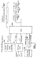
- FIG.23 shows the display generator in block diagram form.
- the signal from the solid state sensor is fed to an analog to a digital converter 342 for converting the analog video into digital video signal.
- the output of analog to the digital converter 342 is fed to a horizontal display generator 344.
- the output from the horizontal display generator 344 is fed to a vertical display generator 346 which provides both horizontally and vertically corrected video output that is fed to digital to an analog converter 348.
- the digital video signals from analog to the digital converter 342 are fed directly to a logic circuit 350 and through a first delay circuit 352 and through a second delay circuit 354.
- a delay circuit 354 consists of three delay lines 356, 358 and 360.
- the output from the delay circuit 354 goes from 0 delay to 3 ⁇ delay means of a sequence sampling switch 362.
- the delay ⁇ in the delay line 352 is one-half a horizontal gate width so that the number of lines in the delay circuit 354 equals one-half of the vertical gate width.
- the output from the horizontal corrected video out of the logic circuit 350 is fed directly to the logic circuit 362 (FIG.25) and through horizontal delay circuits 364 and 366.
- Logic circuits 350 and 362 are controlled by the horizontal and vertical gates and center position signals respectively from the vertical gate generator 334 (FIG.22).
- the delay circuits 354 and 366 consist of a number of a plurality of delay elements which should equal one-half of the vertical gate width. In the example shown there are three delay elements.
- clock pulses corresponding to enlarging magnification are generated in the variable scan generator 316, and reading of signal from the solid state sensor 312 is thereby controlled to execute or stop.
- the display generator 314 When signal is taken from the sensor 312, the display generator 314 generates the signal, and when signal is not taken therefrom, the display generator 314 issues a signal which is delayed by the delay line.
- interpolation between neighboring two picture elements is performed by successively issuing the previous one (or several) signal(s) of picture element or the previous one (or several) signal(s) of line(s). Therefore, the quality of the enlarged picture is deteriorated like a mosaic state.
- horizontal transferring of the sensor which is generally executed with very high speed, is not easily controlled to execute or stop at every time period of the picture element. It may result in deterioration of quality of the image by the reason such as imperfect transferring of data of the CCD.
- the object of the present invention is to offer an image pickup apparatus which can enlarge or reform the image without declining quality of the image through optimum memory means.
- the image pickup apparatus in accordance with the present invention comprises: a solid-state image pickup element; a drive circuit which controls to execute and stop vertical scanning of the image pickup element in response to a control signal C1; n pieces of line memories (M1--Mn) for storing data of scanning lines; change-over means for selectively giving an output signal SO of the image pickup element to the line memories in response to a control signal C2; a selector for selecting output signals of m pieces of the line memories in response to a control signal C3; at least one multiplier for multiplying output signals S1--Sm of the selector by weight signals W1--Wm, respectively; an adder for adding output signals of the multiplier to each other; and a control signal generating circuit which issues the control signals C1, C2, C3 and W1--Wm and controls the change-over means, to execute vertical transferring of the image pickup element, thereby to supply a new line's signal SON and write the new line's signal
- the above-mentioned image pickup apparatus realizes special functions such as enlargement or reform of the picture by using only several line memories without lowering quality of the image.
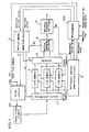
- FIG.1 is a block diagram showing an image pickup apparatus of a first embodiment of the present invention.
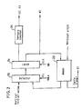
- FIG.2 is a block diagram showing a vertical address generating circuit of the first embodiment.
- FIG.3 is a block diagram showing a horizontal address generating circuit of the first embodiment.
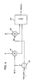
- FIG.4 is a block diagram showing a vertical interpolating circuit of the first embodiment.
- FIG.5 is a block diagram showing a horizontal interpolating circuit of the first embodiment.
- FIG.6(a) and FIG.6(b) are illustrations showing concept of magnification of a picture.
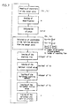
- FIG.7 is a flow-chart showing a process of a microcomputer 220 in accordance with the first embodiment.
- FIG.8 is a block diagram showing a circuit which is constructed by logic circuit to follow the flow-chart of FIG.7.
- FIG.9 is a block diagram showing the image pickup apparatus of a second embodiment of the present invention.
- FIG.10 is a block diagram showing the image pickup apparatus of a third embodiment of the present invention.
- FIG.11 is a block diagram showing a processing circuit of the image pickup apparatus of a fourth embodiment in accordance with the present invention.
- FIG.12 is a block diagram showing a processing circuit of the image pickup apparatus of a fifth embodiment in accordance with the present invention.
- FIG.13 is a block diagram showing the image pickup apparatus of a sixth embodiment of the present invention.
- FIG.14 is a block diagram showing a control signal generating circuit 113 of the sixth embodiment.
- FIG.15 is a block diagram showing the image pickup apparatus of a seventh embodiment of the present invention.
- FIG.16 is a block diagram showing a vertical pitch generating circuit and a vertical address generating circuit of the seventh embodiment.
- FIG.17 is a block diagram showing a horizontal pitch generating circuit and a horizontal address generating circuit of the seventh embodiment.
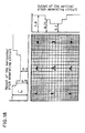
- FIG.18 is a graph showing an example of partially enlarged image and data of ROM 22 and ROM 23.
- FIG.19 is the block diagram showing the conventional image pickup apparatus.
- FIG.20 is the block diagram showing the variable scan generator of the conventional image pickup apparatus.
- FIG.21 is the block diagram showing the horizontal scan generator of the conventional image pickup apparatus.
- FIG.22 is the block diagram showing the vertical scan generator of the conventional image pickup apparatus.
- FIG.23 is the block diagram showing the display generator of the conventional image pickup apparatus.
- FIG.24 is the block diagram showing the horizontal display generator of the conventional image pickup apparatus.
- FIG.25 is the block diagram showing the vertical display generator of the conventional image pickup apparatus.
- FIG.1 is a block diagram showing the image pickup apparatus of a first embodiment.
- a CCD type image pickup element which has a vertical transferring part comprising a construction of shift register, is employed as a solid-state image pickup element 201 and continuous zooming is carried out by means of a microcomputer 220.
- a drive circuit 202 controls to execute or stop vertical-transferring of the solid-state image pickup element 201 in accordance with a control signal C1. Electric charge for unnecessary scanning lines is swept by the drive circuit 202 in accordance with a control signal C4.
- Output signal of the image pickup element 201 is selectively given to line memories 5, 6 and 7 through a change-over switch 4 in response to a control signal C2.
- a selector 8 selects two of the line memories and issues data in response to a control signal C3. Output signal of the selector 8 is sent to a vertical interpolating circuit 9 and a horizontal interpolating circuit 10.
- a vertical address generating circuit 11 receives a vertical initial value and a vertical pitch signal from the microcomputer 220 as input signals. The vertical address generating circuit 11 generates the control signal C1 for controlling vertical transferring of the solid-state image pickup element 201, the control signals C2 and C3 for respectively controlling the change-over switch 4 and the selector 8, and a weight signal W2 for the vertical interpolating circuit 9.
- a horizontal address generating circuit 13 receives a horizontal initial value and a horizontal pitch signal from the microcomputer 220 as input signals.
- the horizontal address generating circuit 13 generates write address and read address for the line memories 5, 6 and 7 and weight signal W4 for the horizontal interpolating circuit 10.
- the vertical address generating circuit 11 and the horizontal address generating circuit 13 constitute a control signal generating circuit. According to random magnification and coordinates of the center of the partial image to be enlarged, the microcomputer 220 calculates to issue signals of the vertical initial value and the horizontal initial value, a vertical pitch and a horizontal pitch, and position of transferring head line of the solid state image pickup element 201.
- FIG.2 is a block diagram showing the vertical address generating circuit 11.
- Initial value is set in a selector 26 during time period of vertical blanking (VBLK), and thereafter an adder 23 adds vertical pitch signals given thereto, at every line.
- Decimal processed in the adder 23 is issued through a latch 24 as the weight signal W2 for the vertical interpolating circuit 9.
- Carry signal of the adder 23 is issued as the control signal C1 and sent to a ternary counter 25.
- the lowest two bits of number processed in the ternary counter 25 are issued as the control signals C2 and C3.
- FIG.3 is a block diagram showing the horizontal address generating circuit 13.
- Initial value is set in a selector 36 during time period of horizontal blanking (HBLK), and thereafter an adder 33 adds horizontal pitch signals given thereto, at every picture element.
- Integer processed in the adder 33 is issued through a latch 34 as a read address signal for the line memories 5, 6 and 7 (FIG.1), and decimal of that is issued through a delay circuit 35 as the weight signal W4 for the horizontal interpolating circuit 10.
- the lowest bit of the integer is inputted to an exclusive OR gate 38 together with signal passed through a latch 37.
- the control signal C5 is issued from the exclusive OR gate 38 to the horizontal interpolating circuit 10 (FIG.1).
- Write addresses for the line memories 5, 6 and 7 are issued from a counter 39.
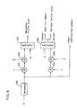
- FIG.4 is a block diagram showing the vertical interpolating circuit 9.
- the circuit 9 comprises multipliers 41 and 42, a subtracter 43 and an adder 44. Two picture element's signals weighed by the multipliers 41 and 42 are added each other by the adder 44 and issued therefrom.
- FIG.5 is a block diagram showing the horizontal interpolating circuit 10.
- the circuit 10 comprises latches 51 and 52, multipliers 53 and 54, an adder 55 and a subtracter 56. Signals of picture elements, which are mutually neighboring signals in the horizontal direction, are taken by the latches 51 and 52. Signals of two picture elements, which are weighted by the multiplier 53 and 54, are added to each other by the adder 55 and issued therefrom.
- FIG.6(a), FIG.6(b) and FIGs. 1--5 For instance, proportional enlargement of 4/3 times in the vertical direction is shown.
- magnification of 4/3 and a central coordinates (Xc, Yc) are predetermined.
- the microcomputer 220 calculates a scanning starting line of the solid-state image pickup element 201 and vertical/horizontal initial values and pitches from the given magnification and the central coordinates, and the microcomputer 220 issues outputs to the drive circuit 202 for the image pickup element 201, the vertical address generating circuit 11 and the horizontal address generating circuit 13. A pitch of 0.75 is given to the vertical address generating circuit 11 in response to the magnification.
- decimal value of the vertical address of the scanning line D which is held by the latch 24, is 0.25
- value of W1 is set to be 0.75 and value of W2 is 0.25
- the multipliers 41 and 42 multiply weights into the scanning lines [3] and [4], respectively, and the weighted signals are added each other in the adder 44, thereby outputting interpolated signals of the scanning line D.
- adding of the next address is executed in the adder 23, and the vertical pitch 0.75 is added to the output 0.25 of the latch 24. Since sum is 1.00 (0.75+0.25), a carry signal C1 becomes 1, and this signal C1 is supplied to the drive circuit 202.
- Decimal 0.00 is written to the latch 24 by a next horizontal pulse HD.
- the drive circuit 202 When the carry signal C1 becomes 1, the drive circuit 202 operates to vertically transfer the solid-state image pickup element 201, and a new signal of the scanning line [5] is issued from the solid-state image pickup element 201.
- a signal of the scanning line [2] stored in the line memory 5 is the oldest one among the signals of the scanning lines [2], [3] and [4]. It has already been unnecessary for interpolation after the scanning line D. Therefore, the change-over switch 4 selects the line memory 5 and operates to write the signal of the scanning line [5] issued from the solid-state image pickup element 201. Both the writing to the line memory and the reading from that, that is, reading of the scanning lines [3] and [4] and writing of the scanning line [5], are simultaneously executed.
- the signal of the scanning line [4] can be used as that of the scanning line E.
- the weight signal W1 supplied to the multiplier 42 is 1, and the weight signal W2 supplied to the multiplier 41 is zero, thereby operating to supply the multiplier 42 and 41 with signals of the scanning line [4] and [5], respectively. That is, the selector 8 issues the signal of the line memory 7 to the multiplier 42 and the signal of the line memory 5 to the multiplier 41.
- the signal of the scanning line [4], namely the scanning line E is therefore issued from the adder 44.
- Table 1 shows the above-mentioned selection of reading/writing of the line memories 5, 6 and 7 and control of transferring of the solid-state image pickup element 201.
- Table 2 shows another selection of reading/writing of the line memories 5, 6 and 7 and another control of transferring of the solid-state image pickup element.
- the control signal C1 is delayed with one line against the operation of Table 1.
- Outputs from the horizontal address generating circuit shown by FIG.3 are used as read addresses for the line memories 5, 6 and 7.
- Output signal from the vertical interpolating circuit 9 is supplied to the horizontal interpolating circuit shown by FIG.5.
- Interpolation between two picture elements in the horizontal direction is executed by using the horizontal weight signal W4 generated by the horizontal address generating circuit shown by FIG.3. This operation is very similar to that of vertical direction.
- the latch 37 and the exclusive OR gate 38 change of the read address is detected. When the change is detected, the control signal C5 becomes 1, and the next picture element's signals are taken into the latches 51 and 52 of the horizontal interpolating circuit 10. Other operation is the same as that of the vertical enlargement.
- the image pickup apparatus of this embodiment can offer an electronic zoom image pickup apparatus which realizes special functions such as enlargement or reform of the picture by means of several line memories without lowering quality of the image. Besides, by changing the magnification given to the microcomputer 220 with lapse of time, continuous zooming like that of an optical zoom lens is obtained. Also, by changing the center of coordinates given to the microcomputer 220 as time lapses, continuous movement of pickup angle, e.g. pan or tilt of the image pickup apparatus, is realized.
- This circuit-unit comprises a circuit 230 for obtaining reciprocal, multipliers 231, 232, 234 and 235 and subtracter 233 and 236.
- the circuit 230 finds a reciprocal p of the magnification m and issues the reciprocal p as vertical/horizontal pitches.
- the multiplier 231 multiplies the pitch p and a number H of the horizontal picture element together, and the multiplier 232 makes output of the multiplier 231 1/2 times.
- the subtracter 233 subtracts the output of the multiplier 232 from a horizontal coordinates Xc of the central coordinates given thereto, and output signal of the subtracter 233 is issued as a horizontal initial value.
- the multiplier 234 multiplies the pitch p by a number V of the scanning lines in one field, and the multiplier 235 makes output of the multiplier 234 1/2 times.
- the subtracter 236 subtracts output of the multiplier 235 from a vertical coordinates Yc of the central coordinates given thereto. Integer of output signal of the subtracter 236 is issued as a starting line number of vertical scanning, and decimal of that is issued as a vertical initial value.
- a processing circuit (not shown) is generally provided between the image pickup element 201 and the change-over switch 4 or at the next step of the block diagram shown by FIG.1 in order to obtain luminance signal and chrominance signal.
- FIG.9 is a block diagram showing the image pickup apparatus of a second embodiment.
- a CCD type image pickup element which has a vertical transferring part comprising a construction of shift register, is employed as a solid-state image pickup element 1.
- a drive circuit 2 controls to execute or stop vertical-transferring of the solid-state image pickup element 1 in accordance with a control signal C1. Electric charge for unnecessary scanning lines is swept by the drive circuit 2 in accordance with a control signal C4.
- Output signal of the solid-state image pickup element 1 is selectively given to line memories 5, 6 and 7 through a change-over switch 4 in response to a control signal C2.
- a selector 8 selects two of the line memories and issues data in response to a control signal C3.
- Output signal of the selector 8 is sent to a vertical interpolating circuit 9 and a horizontal interpolating circuit 10.
- a vertical address generating circuit 11 receives a vertical initial value and a vertical pitch signal as input signals.
- the vertical address generating circuit 11 generates the control signal C1 for controlling vertical transferring of the solid-state image pickup element 1, the control signals C2 and C3 for respectively controlling the change-over switch 4 and the selector 8, and a weight signal W2 for the vertical interpolating circuit 9.
- a horizontal address generating circuit 13 receives a horizontal initial value and a horizontal pitch signal as input signals.
- the horizontal address generating circuit 13 generates write address and read address for the line memories 5, 6 and 7 and weight signal W4 for the horizontal interpolating circuit 10.
- the vertical address generating circuit 11 and the horizontal address generating circuit 13 constitute a control signal generating circuit.
- FIG. 2 is a block diagram shown the vertical address generating circuit 11.
- FIG.3 is a block diagram showing the horizontal address generating circuit 13.
- FIG.4 is a block diagram showing the vertical interpolating circuit 9.
- FIG.5 is a block diagram showing the horizontal interpolating circuit 10. Description concerning these circuits are the same as described in the first embodiment.
- FIG.6(a), FIG.6(b) and FIGs. 1--5 For instance, proportional enlargement of 4/3 times in the vertical direction is shown.
- a pitch of 0.75 corresponding to magnification is predetermined.
- data of scanning lines [2], [3], and [4], which are issued from the solid-state image pickup element 1, are stored, respectively.
- interpolation of a scanning line D is described. Decimal of data which means vertical position of the scanning line D is held by the latch 24.
- the selector 8 operates to issue signal of the line memory 6 and signal of the line memory 7 to the multiplier 42 of the vertical interpolating circuit 9 and the multiplier 41 thereof, respectively. If decimal value of the vertical address of the scanning line D, which is held by the latch 24, is 0.25, value of W1 is set to be 0.75 and value of W2 is 0.25, in the vertical interpolating circuit 9.
- the multipliers 41 and 42 multiply weights on the scanning lines [3] and [4], respectively, and the weighted signals are added each other in the adder 44, thereby outputting interpolated signals of the scanning line D.
- the change-over switch 4 selects the line memory 5 and operates to write the signal of the scanning line [5] issued from the solid-state image pickup element 1. Both writing to the line memory and reading from that, namely reading of the scanning lines [3] and [4] and writing of the scanning line [5], are simultaneously executed.
- the signal of the scanning line [4] can be used as that of the scanning line E.
- the weight signal W1 supplied to the multiplier 42 is 1, and the weight signal W2 supplied to the multiplier 41 is zero, thereby operating to supply the multiplier 42 and 41 with signals of the scanning line [4] and [5], respectively. That is, the selector 8 issues the signal of the line memory 7 to the multiplier 42 and the signal of the line memory 5 to the multiplier 41.
- the signal of the scanning line [4], namely the scanning line E is therefore issued from the adder 44.
- Outputs from the horizontal address generating circuit shown by FIG.3 are used as read addresses for the line memories 5, 6 and 7.
- Output signal from the vertical interpolating circuit 9 is supplied to the horizontal interpolating circuit shown by FIG.5.
- Interpolation between two picture elements in the horizontal direction is executed by using the horizontal weight W4 generated by the horizontal address generating circuit shown by FIG.3. This operation is very similar to that of vertical direction.
- the latch 37 and the exclusive OR gate 38 change of the read address is detected. When the change is detected, the control signal C5 becomes 1, and the next picture element's signals are taken into the latches 51 and 52 of the horizontal interpolating circuit 10. Other operation is the same as that of the vertical enlargement.
- the image pickup apparatus of this embodiment can offer an electronic zoom image pickup apparatus which realizes special functions such as enlargement or reform of the picture by means of several line memories without declining quality of the image.
- FIG.10 is a block diagram showing the image pickup apparatus of a third embodiment.
- This image pickup apparatus has an electronic zooming function and is characterized by providing a processing circuit 3 which generates luminance signal and chrominance signal from output of an image pickup element 1.
- the image pickup element 1 has a vertical transferring part comprising a construction of shift register such as CCD.
- a drive circuit 2 controls to execute or stop vertical-transferring of the solid-state image pickup element 1 in accordance with a control signal C1. Electric charge for unnecessary scanning lines is swept by the drive circuit 2 in accordance with a control signal C4.
- the luminance signal and the chrominance signal or a chrominance-difference signal are obtained from the output signal of the solid state image pickup element 1 by means of the processing circuit 3.
- Output signal of the processing circuit 3 is selectively given to line memories 5, 6 and 7 through a change-over switch 4 in response to a control signal C2.
- a selector 8 selects two of the line memories and issues data in response to a control signal C3.
- Output signal of the selector 8 is sent to a vertical interpolating circuit 9 and a horizontal interpolating circuit 10.
- a vertical address generating circuit 11 receives a vertical initial value and a vertical pitch signal which are preset. The vertical address generating circuit 11 generates the control signal C1 for controlling vertical transferring of the image pickup element 1, the control signals C2 and C3 for respectively controlling the change-over switch 4 and the selector 8, and weight signal W2 for the vertical interpolating circuit 9.
- a horizontal address generating circuit 13 receives a horizontal initial value and a horizontal pitch signal and generates write address and read address for the line memories 5, 6 and 7 and weight signal W4 for the horizontal interpolating circuit 10.
- construction except the processing circuit 3 is the same one as that of the second embodiment (FIG.9). Therefore, electronic enlargement or reform of the luminance signal and the chrominance signal which are obtained by the processing circuit 3 are carried out in the same way as that of the second embodiment.
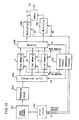
- FIG.11 is a block diagram showing the processing circuit 3 of the image pickup apparatus in accordance with the fourth embodiment.
- a pair of selectors 91 and 92 select input signals of a pair of delay lines 93 and 94 in response to the control signal C1 issued from the vertical address generating circuit 11.
- Each of the delay lines (hereinafter is referred as 1HDL) 93 and 94 delays signal of one horizontal scanning time period.
- a signal generating circuit 95 generates the luminance signal or the chrominance signal by utilizing output signals of the 1HDL 93 and 94 and the solid-state image pickup element 1.
- the selectors 91, 92, the 1HDL 93, 94 and the signal generating circuit 95 constitute the process circuit 3.
- FIG.12 is a block diagram showing the processing circuit 3 of the image pickup apparatus in accordance with the fifth embodiment.
- a drive circuit 96 controls to drive or stop a pair of delay lines 93 and 94 in response to the control signal C1 issued from the vertical address generating circuit 11.
- Each of the delay lines (hereinafter is referred as 1HDL) 93 and 94 delays signal of one horizontal scanning time period.
- a signal generating circuit 95 generates the luminance signal or the chrominance signal by utilizing output signals of the 1HDL 93 and 94 and the solid-state image pickup element 1.
- the drive circuit 96, the 1HDL 93, 94 and the signal generating circuit 95 constitute the processing circuit 3.
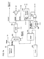
- FIG.13 is a block diagram showing the image pickup apparatus of a sixth embodiment.
- a solid-state image pickup element 101 is of a type which is scanned with X-Y address like a MOS type.
- a drive circuit 102 supplies vertical and horizontal scanning pulses to drive the solid-state image pickup element 101.
- Vertical scanning of the image pickup element 101 is executed or stopped in response to a control signal C1, and a head line number of vertical scanning is determined by a control signal C4.
- Luminance signal and chrominance signal are obtained from output signal of the solid-state image pickup element 101 by means of a processing circuit 103.
- Output signal of the processing circuit 103 is selectively given to line memories 5, 6 and 7 through a change-over switch 104 in response to a control signal C2.
- a selector 108 selects two of the line memories and issues data in response to a control signal C3.
- Multipliers 109 and 110 multiply output signal of the selector 108 by weight signals W1 and W3, respectively. Scanning line's signal of an upper side of the picture is supplied to the multiplier 109, and scanning line's signal of a lower side of the picture is supplied to the multiplier 110.
- An adder 111 adds output signals of the multipliers 109 and 110 each other and issues output signal to an output terminal 112.
- a control signal generating circuit 113 supplies the control signals and the weight signals to each part and also supplies the address signals to the line memories 5, 6 and 7.
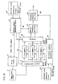
- FIG.14 is a block diagram showing the control signal generating circuit 113.
- a starting address register 121 specifies a starting position of the scanning lines for a desired part of the picture to be enlarged. For example, interval between the scanning lines in respective fields is selected to be 1. Integer of the starting address is issued as a starting line number C4 of vertical scanning, and decimal of the starting address is issued to a selector 123.
- a pitch register 122 specifies a value which is converted from interval of the scanning lines of an enlarged picture to that of an original picture. When the picture is enlarged, the above-mentioned value is below 1.
- the selector 123 issues the initial value from the starting address register 121 during the vertical blanking, and issues the signal from the adder 125 except the time of vertical blanking, thereby to form a looped circuit by the selector 123, the latch 124 and the adder 125.
- a latch 124 latches input signal once at each line.
- An adder 125 adds output of the latch 124 with output of the pitch register 122.
- a carry signal is issued as C1 and other lower digits of the signal is issued to the selector 123.
- a ternary counter 126 counts HD only at the time when value of C1 is 1, thereby issuing counting value as C2 and C3.
- Output signal of the latch 124 is used as a weight signal W2 (0 ⁇ W2 ⁇ 1).
- the selector 108 operates to issue signal of the line memory 6 and signal of the line memory 7 to the multiplier 109 and the multiplier 110, respectively. If decimal value of the vertical address of the scanning line D, which is held by the latch 124, is 0.25, value of W1 is set to be 0.75 and value of W2 is 0.25, in the control signal generating circuit 113.
- the multipliers 109 and 110 multiply weights on the scanning lines [3] and [4], respectively, and the weighted signals are added each other in the adder 111, thereby outputting interpolated signals of the scanning line D. At that time, adding of the next address is executed in the adder 125, and the pitch 0.75 of the pitch register 122 is added to the output 0.25 of the latch 124.
- a carry signal C1 becomes 1, and this signal C1 is supplied to the drive circuit 102. Decimal 0.00 is written to the latch 124 by a next horizontal pulse HD.
- the drive circuit 102 operates to scan the next line of the solid-state image pickup element 101, and a new signal of the scanning line [5] is issued from the solid-state image pickup element 101.
- a signal of the scanning line [2] stored in the line memory 5 is the oldest one among the signals of the scanning lines [2], [3] and [4]. It has already been unnecessary for interpolation after the scanning line D.
- the change-over switch 104 selects the line memory 5 and operates to write the signal of the scanning line [5] issued from the solid-state image pickup element 101. Both writing to the line memory and reading from that, namely reading of the scanning lines [3] and [4] and writing of the scanning line [5], are simultaneously executed.
- the signal of the scanning line [4] can be used as that of the scanning line E.
- the weight signal W1 supplied to the multiplier 109 is 1, and the weight signal W2 supplied to the multiplier 110 is zero, thereby operating to supply the multiplier 109 and 110 with signals of the scanning line [4] and [5], respectively. That is, the selector 108 issues the signal of the line memory 7 to the multiplier 109 and the signal of the line memory 5 to the multiplier 110.
- the signal of the scanning line [4], namely the scanning line E is therefore issued from the adder 111.
- FIG.15 is a block diagram showing the image pickup apparatus of a seventh embodiment.
- a drive circuit 2 controls to execute or stop vertical-transferring of the solid-state image pickup element 1 in accordance with a control signal C1.
- Output signal of the solid-state image pickup element 1 is selectively given to line memories 5, 6 and 7 through a charge-over switch 4 in response to control signal C2.
- a selector 8 selects two of the line memories and issues data in response to a control signal C3. Output signal of the selector 8 is sent to a vertical interpolating circuit 9 and a horizontal interpolating circuit 10.
- a vertical address generating circuit 11 receives a vertical initial value and a vertical pitch signal given from the vertical pitch generating circuit 12 at every line as input signals.
- the vertical address generating circuit 11 generates the control signal C1 for controlling vertical transferring of the solid-state image pickup element 1, the control signals C2 and C3 for respectively controlling the change-over switch 4 and the selector 8, and a weight signal W2 for the vertical interpolating circuit 9.
- a horizontal address generating circuit 13 receives a horizontal initial value and a horizontal pitch signal given from the horizontal pitch generating circuit 14 at every picture element as input signals.
- the horizontal address generating circuit 13 generates write address and read address for the line memories 5, 6 and 7 and weight signal W4 for the horizontal interpolating circuit 10.
- the vertical address generating circuit 11 and the horizontal address generating circuit 13 constitute a control signal generating circuit.
- FIG.16 is a block diagram showing the vertical pitch generating circuit 12 and the vertical address generating circuit 11.
- a counter 21 counts up at every line and is reset during a time period of vertical blanking. Output of the counter 21 is supplied to a ROM 22 as address signals. Data of vertical pitches are stored in the ROM 22 in correspondence with each line of the picture, and the data of vertical pitches are issued in response to the address signal.
- Initial value is set in an adder 23 by a selector 26 during the time period of vertical blanking, and thereafter vertical pitch signal, which is supplied from the ROM 22, is added at every line.
- Decimal processed in the adder 23 is issued through a latch 24 as a weight signal W2 for the vertical interpolating circuit 9.
- Carry signal of the adder 23 is issued as a control signal C1 and sent to a ternary counter 25. The lowest two bits of number processed in the ternary counter 25 are issued as control signals C2 and C3.
- FIG.17 is a block diagram showing the horizontal pitch generating circuit 14 and the horizontal address generating circuit 13.
- a counter 31 counts up at every picture element and is reset during a time period of horizontal blanking. Output of the counter 31 is supplied to a ROM 32 as address signals. Horizontal pitches are stored in the ROM 32 in correspondence with each picture element on the scanning line of the picture, and the horizontal pitches are issued in response to the address signal. Initial value is set in an adder 33 by a selector 36 during the time period of horizontal blanking, and thereafter horizontal pitch signal, which is supplied from the ROM 32, is added at every picture element.
- Integer processed in the adder 33 is issued through the latch 34 as read address signals for the line memories 5, 6 and 7, and decimal processed in the adder 33 is issued through a delay circuit 35 as the weight signal W4 for the horizontal interpolating circuit 10.
- the lowest bit of the integer is inputted to an exclusive OR gate 38 together with signal passed through a latch 37, thereby issuing a control signal C5 to the horizontal interpolating circuit 10.
- a counter 39 has the similar function to that of the counter 31 and generates write addresses for the line memories 5, 6 and 7.
- the selector 8 operates to issue signal of the line memory 6 and signal of the line memory 7 to the multiplier 42 of the vertical interpolating circuit 9 and the multiplier 41 thereof, respectively. If decimal value of the vertical address of the scanning line D, which is held by the latch 24, is 0.25, value of W1 is set to be 0.75 and value of W2 is 0.25, in the vertical interpolating circuit 9.
- the multipliers 41 and 42 multiply weights on the scanning lines [3] and [4], respectively, and the weighted signals are added each other in the adder 44, thereby outputting interpolated signals of the scanning line D.
- the change-over switch 4 selects the line memory 5 and operates to write the signal of the scanning line [5] issued from the solid-state image pickup element 1. Both the writing to the line memory and the reading from that, that is, reading of the scanning lines [3] and [4] and writing of the scanning line [5], are simultaneously executed.
- the signal of the scanning line [4] can be used as that of the scanning line E.
- the weight signal W1 supplied to the multiplier 42 is 1, and the weight signal W2 supplied to the multiplier 41 is zero, thereby operating to supply the multiplier 42 and 41 with signals of the scanning line [4] and [5], respectively. That is, the selector 8 issues the signal of the line memory 7 to the multiplier 42 and the signal of the line memory 5 to the multiplier 41.
- the signal of the scanning line [4], namely the scanning line E is therefore issued from the adder 44.
- Outputs from the horizontal address generating circuit shown by FIG.3 are used as read addresses for the line memories 5, 6 and 7.
- Output signal from the vertical interpolating circuit 9 is supplied to the horizontal interpolating circuit shown by FIG.5.
- Interpolation between two picture elements in the horizontal direction is executed by using the horizontal weight signal W4 generated by the horizontal address generating circuit shown by FIG.3. This operation is very similar to that of vertical direction.
- the latch 37 and the exclusive OR gate 38 change of the read address is detected. When the change is detected, the control signal C5 becomes 1, and the next picture element's signals are taken into the latches 51 and 52 of the horizontal interpolating circuit 10. Other operation is the same as that of the vertical enlargement.
- the ROM which is used for the vertical/horizontal pitch generating circuit
- the ROM can be replaced by a RAM etc.
- various reforming patterns can be easily realized by changing data stored therein.
- the vertical/horizontal pitch generating circuit can be constructed by many logical components.
- the image pickup apparatus of this embodiment can offer an electronic zoom image pickup apparatus which realizes special functions such as enlargement or reform of the picture by means of several line memories without lowering quality of the image.
Landscapes
- Engineering & Computer Science (AREA)
- Multimedia (AREA)
- Signal Processing (AREA)
- Transforming Light Signals Into Electric Signals (AREA)
Claims (9)
- Eine Bildaufnahmevorrichtung, enthaltend:
ein Festkörper-Bildaufnahmeelement (1, 101, 201);
einen Treiberschaltkreis (2, 102, 202), der steuert zum Ausführen und Stoppen der Vertikalabtastung dieses Bildaufnahmeelements, ansprechend auf ein Steuersignal C1;
n Stück Zeilenspeicher (M1--Mn) zum Abspeichern von Daten der Abtastzeilen;
eine Umschalteinrichtung (4, 104) zur selektiven Ausgabe eines Ausgangssignals SO dieses Bildaufnahmeelements zu diesen Zeilenspeichern, ansprechend auf ein Steuersignal C2;
einen Wähler (8, 108) zum Wählen von Ausgangssignalen von m Stück dieser Zeilenspeicher, ansprechend auf ein Steuersignal C3;
wenigstens einen Multiplizierer (41, 42, 109, 110) zum Multiplizieren der Ausgangssignale S1--Sm dieses Wählers mit entsprechenden Wichtungssignalen W1--Wm;
einen Addierer (44, 111) zum Addieren der Ausgangssignale dieses Multiplizierers miteinander; und
einen steuersignalgenerierenden Schaltkreis (11, 13, 113), der diese Steuersignale C1, C2, C3 und W1--Wm ausgibt und diese Umschalteinrichtung steuert, um eine Vertikalübertragung dieses Bildaufnahmeelements auszuführen und dabei ein Signal einer neuen Zeile SON zu liefern und das Signal der neuen Zeile SON in einem Zeilenspeicher Mx zu schreiben, der aus diesen Zeilenspeichern M1--Mn ausgewählt wurde, wobei das in diesem Zeilenspeicher Mx abgespeicherte Signal das älteste der in diesen Zeilenspeichern M1--Mn abgespeicherten Signale ist; wobei
n, m und x die folgenden Beziehungen haben:
n ≧ 3,
2 ≦ m < n,
1 ≦ x ≦ n,
wobei
n, m und x ganze Zahlen sind. - Eine Bildaufnahmevorrichtung gemäß Anspruch 1, die ferner aufweist:
einen Verarbeitungsschaltkreis (3, 103) zum Generieren eines Leuchtdichtesignals oder eines Chrominanz/Chrominanz-Differenz-Signals, die als Eingangssignale der Umschalteinrichtung von diesem Ausgangssignal SO benutzt werden. - Eine Bildaufnahmevorrichtung gemäß Anspruch 2, in der dieser Verarbeitungsschaltkreis eine Verzögerungsleitung (93, 94) aufweist, der ein Ausgangssignal zu der Zeit wieder eingegeben wird, wenn die Vertikalübertragung dieses Bildaufnahmeelements stoppt und dieses Signal SO nicht ausgegeben wird.
- Eine Bildaufnahmevorrichtung gemäß Anspruch 2, in der dieser Verarbeitungsschaltkreis eine Verzögerungsleitung (93, 94) aufweist, wobei das Treiben von dieser ein vorliegendes Signal stoppt und hält zu der Zeit, wenn die Vertikalübertragung dieses Bildaufnahmeelements stoppt und dieses Signal SO nicht ausgegeben wird.
- Eine Bildaufnahmevorrichtung gemäß Anspruch 1, bei der dieses Bildaufnahmeelement einen Vertikalübertragungsteil enthält, der von einem Schieberegister gebildet wird.
- Eine Bildaufnahmevorrichtung gemäß Anspruch 1, bei der dieses Bildaufnahmeelement vom X - Y-Adressentyp ist.
- Eine Bildaufnahmevorrichtung enthaltend:
ein Festkörper-Bildaufnahmeelement (1, 101, 201);
einen Treiberschaltkreis (2, 102, 202), der steuert zum Ausführen und Stoppen der Vertikalabtastung dieses Bildaufnahmeelements, ansprechend auf ein Steuersignal C1;
n Stück Zeilenspeicher (M1--Mn) zum Abspeichern von Daten der Abtastzeilen;
eine Umschalteinrichtung (4, 104) zur selektiven Ausgabe eines Ausgangssignals SO dieses Bildaufnahmeelements zu diesen Zeilenspeichern, ansprechend auf ein Steuersignal C2;
einen Wähler (8, 108) zum Wählen von Ausgangssignalen von m Stück dieser Zeilenspeicher, ansprechend auf ein Steuersignal C3;
wenigstens einen Multiplizierer (41, 42, 109, 110) zum Multiplizieren der Ausgangssignale S1--Sm dieses Wählers mit entsprechenden Wichtungssignalen W1--Wm;
einen Addierer (44, 111) zum Addieren der Ausgangssignale dieses Multiplizierers miteinander;
einen abstands- bzw. grundmaßgenerierenden Schaltkreis (12, 14) zur Ausgabe von Abstands- bzw. Grundmaßsignalen eines vorgegebenen Musters, wobei diese Abstandssignale jeweils den Abtastzeilen eines Bildes entsprechen; und
einen steuersignalgenerierenden Schaltkreis (11, 13, 113), der diese Steuersignale C1, C2, C3 und W1--Wm ausgibt und diese Umschalteinrichtung steuert, um eine Vertikalübertragung dieses Bildaufnahmeelements auszuführen und dabei ein Signal einer neuen Zeile SON zu liefern und das Signal der neuen Zeile SON in einen Zeilenspeicher Mx zu schreiben, der aus diesen Zeilenspeichern M1--Mn ausgewählt wurde, wobei das in diesem Zeilenspeicher Mx abgespeicherte Signal das älteste der in diesen Zeilenspeichern M1--Mn abgespeicherten Signale ist; wobei
n, m und x die folgenden Beziehungen haben:
n ≧ 3,
2 ≦ m < n,
1 ≦ x ≦ n,
wobei
n, m und x ganze Zahlen sind. - Eine Bildaufnahmevorrichtung, aufweisend:
ein Festkörper-Bildaufnahmeelement (1, 101, 201);
einen Treiberschaltkreis (2, 102, 202), der steuert zum Ausführen und Stoppen der Vertikalabtastung dieses Bildaufnahmeelements, ansprechend auf ein Steuersignal C1;
n Stück Zeilenspeicher (M1--Mn) zum Abspeichern von Daten der Abtastzeilen;
eine Umschalteinrichtung (4, 104) zur selektiven Ausgabe eines Ausgangssignals SO dieses Bildaufnahmeelements zu diesen Zeilenspeichern, ansprechend auf ein Steuersignal C2;
einen Wähler (8, 108) zum Wählen von Ausgangssignalen von m Stück dieser Zeilenspeicher, ansprechend auf ein Steuersignal C3;
wenigstens einen Multiplizierer (41, 42, 109, 110) zum Multiplizieren der Ausgangssignale S1--Sm dieses Wählers mit entsprechenden Wichtungssignalen W1--Wm;
einen Addierer (44, 111) zum Addieren der Ausgangssignale dieses Multiplizierers miteinander;
einen Mikrocomputer (220) zum Generieren von Abstands- bzw. Grundmaßsignalen, ansprechend auf ein Vergrößerungssignal, das vorgegeben ist und sich mit dem Ablauf der Zeit ändert; und
einen steuersignalgenerierenden Schaltkreis (11, 13, 113), der diese Steuersignale C1, C2, C3 und W1--Wm ausgibt und diese Umschalteinrichtung steuert, um eine Vertikalübertragung dieses Bildaufnahmeelements auszuführen und dabei ein Signal einer neuen Zeile SON zu liefern und das neue Zeilensignal SON in einem Zeilenspeicher Mx zu schreiben, der aus diesen Zeilenspeichern M1--Mn ausgewählt wurde, wobei das in diesem Zeilenspeicher Mx abgespeicherte Signal das älteste der in diesen Zeilenspeichern M1--Mn abgespeicherten Signale ist; wobei
n, m und x die folgenden Beziehungen haben:
n ≧ 3,
2 ≦ m < n,
1 ≦ x ≦ n,
wobei
n, m und x ganze Zahlen sind. - Eine Bildaufnahmevorrichtung, aufweisend:
ein Festkörper-Bildaufnahmeelement (1, 101, 201), das einen Vertikalübertragungsteil aufweist, der von einem Schieberegister gebildet wird;
einen Treiberschaltkreis (2, 102, 202), der steuert zum Ausführen und Stoppen des Vertikalabtastens dieses Bildaufnahmeelements, ansprechend auf ein Steuersignal C1;
einen Verarbeitungsschaltkreis (3, 103) zum Generieren eines Leuchtdichtesignals oder eines Chrominanz/Chrominanz-Differenz-Signals aus einem Ausgangssignal SO dieses Bildaufnahmeelements;
n Stück Zeilenspeicher (M1--Mn) zum Abspeichern von Daten der Abtastzeilen;
eine Umschalteinrichtung (4, 104) zur selektiven Ausgabe des Ausgangssignals dieses Verarbeitungsschaltkreises zu diesen Zeilenspeichern, ansprechend auf ein Steuersignal C2;
einen Wähler (8, 108) zum Wählen von Ausgangssignalen von m Stück dieser Zeilenspeicher, ansprechend auf ein Steuersignal C3;
wenigstens einen Multiplizierer (41, 42, 109, 110) zum Multiplizieren der Ausgangssignale S1--Sm dieses Wählers mit entsprechenden Wichtungssignalen W1--Wm;
einen Addierer (44, 111) zum Addieren der Ausgangssignale dieses Multiplizierers miteinander;
einen Mikrocomputer (220) zum Generieren von Abstands- bzw. Grundmaßsignalen, ansprechend auf ein Vergrößerungssignal, das vorgegeben ist und sich mit dem Ablauf der Zeit ändert; und
einen steuersignalgenerierenden Schaltkreis (11, 13, 113), der diese Steuersignale C1, C2, C3 und W1--Wm ausgibt und diese Umschaltmittel steuert, um eine Vertikalübertragung dieses Bildaufnahmeelements auszuführen und dabei ein Signal einer neuen Zeile SON zu liefern und das Signal der neuen Zeile SON in einem Zeilenspeicher Mx abzuspeichern, der aus diesen Zeilenspeichern M1--Mn ausgewählt wurde, wobei das in diesem Zeilenspeicher Mx abgespeicherte Signal das älteste der in diesen Zeilenspeichern M1--Mn abgespeicherten Signale ist; wobei
n, m und x die folgenden Beziehungen haben:
n ≧ 3,
2 ≦ m < n,
1 ≦ x ≦ n,
wobei
n, m und x ganze Zahlen sind.
Applications Claiming Priority (6)
| Application Number | Priority Date | Filing Date | Title |
|---|---|---|---|
| JP63089827A JPH0767154B2 (ja) | 1988-04-12 | 1988-04-12 | 撮像装置 |
| JP89827/88 | 1988-04-12 | ||
| JP184320/88 | 1988-07-22 | ||
| JP63184320A JPH0233271A (ja) | 1988-07-22 | 1988-07-22 | 撮像装置 |
| JP289297/88 | 1988-11-16 | ||
| JP63289297A JPH02135880A (ja) | 1988-11-16 | 1988-11-16 | 撮像装置 |
Publications (2)
| Publication Number | Publication Date |
|---|---|
| EP0337424A1 EP0337424A1 (de) | 1989-10-18 |
| EP0337424B1 true EP0337424B1 (de) | 1993-09-29 |
Family
ID=27306250
Family Applications (1)
| Application Number | Title | Priority Date | Filing Date |
|---|---|---|---|
| EP89106506A Expired - Lifetime EP0337424B1 (de) | 1988-04-12 | 1989-04-12 | Bildaufnahmegerät |
Country Status (4)
| Country | Link |
|---|---|
| US (1) | US4951125A (de) |
| EP (1) | EP0337424B1 (de) |
| KR (1) | KR920006956B1 (de) |
| DE (1) | DE68909470T2 (de) |
Families Citing this family (23)
| Publication number | Priority date | Publication date | Assignee | Title |
|---|---|---|---|---|
| US5083208A (en) * | 1988-12-26 | 1992-01-21 | Ricoh Company, Ltd. | Electronic zoom apparatus |
| JPH0393370A (ja) * | 1989-09-06 | 1991-04-18 | Nippon Hoso Kyokai <Nhk> | 画像処理装置 |
| JPH03282497A (ja) * | 1990-03-30 | 1991-12-12 | Toshiba Corp | 信号変換方式および装置 |
| JP2913797B2 (ja) * | 1990-08-10 | 1999-06-28 | ソニー株式会社 | 画像拡縮処理方法 |
| KR940007161B1 (ko) * | 1991-06-21 | 1994-08-06 | 삼성전자 주식회사 | 이미지버퍼를 이용한 전자주밍시스템 |
| US5138454A (en) * | 1991-09-16 | 1992-08-11 | Eastman Kodak Company | Megapixel video previewer framestore and display |
| US5333055A (en) * | 1992-02-24 | 1994-07-26 | Sanyo Electric Co., Ltd. | Video camera circuit for processing image signals from an image pickup device having a mosaic color filter |
| US5565919A (en) * | 1992-03-12 | 1996-10-15 | Hitachi, Ltd. | Video camera/VTR and camera station with opto-electronic link between camera/VTR and camera station |
| JP3216907B2 (ja) * | 1992-05-18 | 2001-10-09 | 株式会社日立製作所 | 電子ズーム装置及び撮像装置 |
| WO1994003015A1 (en) * | 1992-07-22 | 1994-02-03 | Matsushita Electric Industrial Co., Ltd. | Imaging device with horizontal line interpolation function |
| GB2269955B (en) * | 1992-08-07 | 1996-02-14 | British Broadcasting Corp | Method of showing 16:9 pictures on 4:3 displays |
| US5481304A (en) * | 1992-09-25 | 1996-01-02 | Samsung Electronics Co., Ltd. | Apparatus for zooming a digital video signal of a predetermined color order which is derived from a charge-coupled device |
| US5406334A (en) * | 1993-08-30 | 1995-04-11 | Sony Corporation | Apparatus and method for producing a zoomed image signal |
| JP2931520B2 (ja) * | 1993-08-31 | 1999-08-09 | 三洋電機株式会社 | 単板式カラービデオカメラの色分離回路 |
| TW269091B (de) * | 1993-12-22 | 1996-01-21 | Matsushita Electric Industrial Co Ltd | |
| US5428390A (en) * | 1994-01-21 | 1995-06-27 | Texas Instruments Incorporated | Apparatus and method for focal plane zoom and pan |
| US5903481A (en) * | 1994-09-09 | 1999-05-11 | Sony Corporation | Integrated circuit for processing digital signal |
| US6509927B1 (en) * | 1994-12-16 | 2003-01-21 | Hyundai Electronics America Inc. | Programmably addressable image sensor |
| US6380979B1 (en) | 1996-07-02 | 2002-04-30 | Matsushita Electric Industrial Co., Ltd. | Scanning line converting circuit and interpolation coefficient generating circuit |
| MY119346A (en) | 1996-12-24 | 2005-05-31 | Sony Corp | Picture processing apparatus and method |
| JP5030261B2 (ja) * | 2005-11-16 | 2012-09-19 | キヤノン株式会社 | 映像配信装置、ビューワ装置、映像配信装置の制御方法、ビューワ装置の制御方法およびコンピュータプログラム |
| JP2008035324A (ja) * | 2006-07-31 | 2008-02-14 | Matsushita Electric Ind Co Ltd | 撮像装置 |
| JP6412361B2 (ja) | 2014-07-30 | 2018-10-24 | Hoya株式会社 | 内視鏡用撮像装置 |
Family Cites Families (15)
| Publication number | Priority date | Publication date | Assignee | Title |
|---|---|---|---|---|
| US3935381A (en) * | 1974-06-24 | 1976-01-27 | The United States Of America As Represented By The Secretary Of The Navy | Electronic solid state sensor image size control |
| US4002824A (en) * | 1976-01-28 | 1977-01-11 | The United States Of America As Represented By The Secretary Of The Navy | Selective zoom camera and display |
| JPS5397328A (en) * | 1977-02-07 | 1978-08-25 | Toshiba Corp | Electronic zooming system for charge transfer type pickup element |
| JPS58207776A (ja) * | 1982-05-28 | 1983-12-03 | Victor Co Of Japan Ltd | 撮像装置 |
| JPS5915370A (ja) * | 1982-07-16 | 1984-01-26 | Canon Inc | 信号処理装置 |
| GB8410596D0 (en) * | 1984-04-25 | 1984-05-31 | Quantel Ltd | Video signal processing |
| JPS61121068A (ja) * | 1984-11-16 | 1986-06-09 | Toshiba Corp | 画像形成装置 |
| JPS61232781A (ja) * | 1985-04-05 | 1986-10-17 | Matsushita Electric Ind Co Ltd | 固体撮像装置 |
| JPS6259473A (ja) * | 1985-09-09 | 1987-03-16 | Toshiba Corp | 固体撮像装置 |
| JPS62132489A (ja) * | 1985-12-04 | 1987-06-15 | Matsushita Electric Ind Co Ltd | 固体撮像装置 |
| JPS62291269A (ja) * | 1986-06-11 | 1987-12-18 | Toshiba Corp | 固体カラ−撮像装置 |
| JPS6386975A (ja) * | 1986-09-30 | 1988-04-18 | Toshiba Corp | 固体カラ−撮像装置 |
| JP2557866B2 (ja) * | 1987-01-28 | 1996-11-27 | キヤノン株式会社 | 固体撮像装置 |
| JP2557865B2 (ja) * | 1987-01-28 | 1996-11-27 | キヤノン株式会社 | 固体撮像装置 |
| JPS63185285A (ja) * | 1987-01-28 | 1988-07-30 | Canon Inc | 固体撮像装置 |
-
1989
- 1989-04-12 US US07/336,490 patent/US4951125A/en not_active Expired - Lifetime
- 1989-04-12 EP EP89106506A patent/EP0337424B1/de not_active Expired - Lifetime
- 1989-04-12 KR KR8904857A patent/KR920006956B1/ko not_active Expired
- 1989-04-12 DE DE89106506T patent/DE68909470T2/de not_active Expired - Fee Related
Also Published As
| Publication number | Publication date |
|---|---|
| KR890016612A (ko) | 1989-11-29 |
| US4951125A (en) | 1990-08-21 |
| KR920006956B1 (en) | 1992-08-22 |
| DE68909470T2 (de) | 1994-02-10 |
| DE68909470D1 (de) | 1993-11-04 |
| EP0337424A1 (de) | 1989-10-18 |
Similar Documents
| Publication | Publication Date | Title |
|---|---|---|
| EP0337424B1 (de) | Bildaufnahmegerät | |
| EP0579795B1 (de) | Digitales bildinterpolationssystem für zoom und schwenkeffekte | |
| US5253064A (en) | Video camera apparatus with electronic zoom control and method therefor | |
| US20090251577A1 (en) | Image sensing apparatus | |
| GB2139456A (en) | Line structure correction circuit | |
| JPS6318394B2 (de) | ||
| EP0629044B1 (de) | Digitale Signalverarbeitung | |
| JPH07111561A (ja) | 原稿読み取り装置 | |
| JPH1021387A (ja) | 画像処理装置および処理方法 | |
| US5157481A (en) | Registration and contour correction circuit and method for solid-state camera | |
| US5153728A (en) | Image enlargement apparatus using plural diverse capacity memories | |
| US7142236B2 (en) | Digital zoom apparatus to perform zoom during successive changes in zoom magnification | |
| US6917383B2 (en) | Image sensing device | |
| US5181110A (en) | Video signal processing circuit capable of enlarging and displaying a picture | |
| EP0851388B1 (de) | Bildverarbeitungsgerät und -verfahren | |
| JP3415215B2 (ja) | ディジタルズーミングシステム | |
| JPH0224073B2 (de) | ||
| US20060237630A1 (en) | Imaging apparatus | |
| JPS6259473A (ja) | 固体撮像装置 | |
| JP2552742B2 (ja) | 適応型輪郭補正回路 | |
| US5481304A (en) | Apparatus for zooming a digital video signal of a predetermined color order which is derived from a charge-coupled device | |
| JPH0233271A (ja) | 撮像装置 | |
| JP3389385B2 (ja) | ビデオカメラ | |
| JP3151288B2 (ja) | 画像要素変換処理装置 | |
| JPH06350876A (ja) | 撮像装置 |
Legal Events
| Date | Code | Title | Description |
|---|---|---|---|
| PUAI | Public reference made under article 153(3) epc to a published international application that has entered the european phase |
Free format text: ORIGINAL CODE: 0009012 |
|
| 17P | Request for examination filed |
Effective date: 19890412 |
|
| AK | Designated contracting states |
Kind code of ref document: A1 Designated state(s): DE GB |
|
| 17Q | First examination report despatched |
Effective date: 19920313 |
|
| GRAA | (expected) grant |
Free format text: ORIGINAL CODE: 0009210 |
|
| AK | Designated contracting states |
Kind code of ref document: B1 Designated state(s): DE GB |
|
| REF | Corresponds to: |
Ref document number: 68909470 Country of ref document: DE Date of ref document: 19931104 |
|
| PLBE | No opposition filed within time limit |
Free format text: ORIGINAL CODE: 0009261 |
|
| STAA | Information on the status of an ep patent application or granted ep patent |
Free format text: STATUS: NO OPPOSITION FILED WITHIN TIME LIMIT |
|
| 26N | No opposition filed | ||
| REG | Reference to a national code |
Ref country code: GB Ref legal event code: IF02 |
|
| PGFP | Annual fee paid to national office [announced via postgrant information from national office to epo] |
Ref country code: DE Payment date: 20070405 Year of fee payment: 19 |
|
| PGFP | Annual fee paid to national office [announced via postgrant information from national office to epo] |
Ref country code: GB Payment date: 20070411 Year of fee payment: 19 |
|
| GBPC | Gb: european patent ceased through non-payment of renewal fee |
Effective date: 20080412 |
|
| PG25 | Lapsed in a contracting state [announced via postgrant information from national office to epo] |
Ref country code: DE Free format text: LAPSE BECAUSE OF NON-PAYMENT OF DUE FEES Effective date: 20081101 |
|
| PG25 | Lapsed in a contracting state [announced via postgrant information from national office to epo] |
Ref country code: GB Free format text: LAPSE BECAUSE OF NON-PAYMENT OF DUE FEES Effective date: 20080412 |