EP0336498B1 - Halbleiterspeicheranordnung - Google Patents
Halbleiterspeicheranordnung Download PDFInfo
- Publication number
- EP0336498B1 EP0336498B1 EP89200807A EP89200807A EP0336498B1 EP 0336498 B1 EP0336498 B1 EP 0336498B1 EP 89200807 A EP89200807 A EP 89200807A EP 89200807 A EP89200807 A EP 89200807A EP 0336498 B1 EP0336498 B1 EP 0336498B1
- Authority
- EP
- European Patent Office
- Prior art keywords
- voltage
- gate
- source zone
- memory
- charge
- Prior art date
- Legal status (The legal status is an assumption and is not a legal conclusion. Google has not performed a legal analysis and makes no representation as to the accuracy of the status listed.)
- Expired - Lifetime
Links
- 239000004065 semiconductor Substances 0.000 title claims description 21
- 230000015654 memory Effects 0.000 claims abstract description 50
- 230000006641 stabilisation Effects 0.000 claims abstract description 6
- 238000011105 stabilization Methods 0.000 claims abstract description 6
- 239000002800 charge carrier Substances 0.000 claims description 4
- 230000005669 field effect Effects 0.000 claims description 2
- 238000010586 diagram Methods 0.000 description 6
- 238000000034 method Methods 0.000 description 6
- 239000003990 capacitor Substances 0.000 description 5
- 239000000758 substrate Substances 0.000 description 3
- 238000010276 construction Methods 0.000 description 2
- 238000005516 engineering process Methods 0.000 description 2
- XUIMIQQOPSSXEZ-UHFFFAOYSA-N Silicon Chemical compound [Si] XUIMIQQOPSSXEZ-UHFFFAOYSA-N 0.000 description 1
- 230000003321 amplification Effects 0.000 description 1
- 230000015572 biosynthetic process Effects 0.000 description 1
- 230000001419 dependent effect Effects 0.000 description 1
- 238000001514 detection method Methods 0.000 description 1
- 230000000694 effects Effects 0.000 description 1
- 238000003199 nucleic acid amplification method Methods 0.000 description 1
- 229910052710 silicon Inorganic materials 0.000 description 1
- 239000010703 silicon Substances 0.000 description 1
- 239000003381 stabilizer Substances 0.000 description 1
Images


Classifications
-
- G—PHYSICS
- G11—INFORMATION STORAGE
- G11C—STATIC STORES
- G11C19/00—Digital stores in which the information is moved stepwise, e.g. shift registers
- G11C19/28—Digital stores in which the information is moved stepwise, e.g. shift registers using semiconductor elements
-
- G—PHYSICS
- G11—INFORMATION STORAGE
- G11C—STATIC STORES
- G11C19/00—Digital stores in which the information is moved stepwise, e.g. shift registers
- G11C19/28—Digital stores in which the information is moved stepwise, e.g. shift registers using semiconductor elements
- G11C19/282—Digital stores in which the information is moved stepwise, e.g. shift registers using semiconductor elements with charge storage in a depletion layer, i.e. charge coupled devices [CCD]
- G11C19/285—Peripheral circuits, e.g. for writing into the first stage; for reading-out of the last stage
-
- G—PHYSICS
- G11—INFORMATION STORAGE
- G11C—STATIC STORES
- G11C11/00—Digital stores characterised by the use of particular electric or magnetic storage elements; Storage elements therefor
- G11C11/21—Digital stores characterised by the use of particular electric or magnetic storage elements; Storage elements therefor using electric elements
- G11C11/34—Digital stores characterised by the use of particular electric or magnetic storage elements; Storage elements therefor using electric elements using semiconductor devices
- G11C11/40—Digital stores characterised by the use of particular electric or magnetic storage elements; Storage elements therefor using electric elements using semiconductor devices using transistors
- G11C11/401—Digital stores characterised by the use of particular electric or magnetic storage elements; Storage elements therefor using electric elements using semiconductor devices using transistors forming cells needing refreshing or charge regeneration, i.e. dynamic cells
- G11C11/4063—Auxiliary circuits, e.g. for addressing, decoding, driving, writing, sensing or timing
- G11C11/407—Auxiliary circuits, e.g. for addressing, decoding, driving, writing, sensing or timing for memory cells of the field-effect type
- G11C11/4074—Power supply or voltage generation circuits, e.g. bias voltage generators, substrate voltage generators, back-up power, power control circuits
Definitions
- the invention relates to a semiconductor memory device comprising a source zone located at a surface of a semiconductor body, a memory gate located beside the source zone and insulated from the surface, by means of which a potential well can be induced in the semiconductor body, in which well an information-representing charge packet in the form of a quantity of charge carriers supplied by the source zone can be stored, and a switching gate located between the source zone and the memory gate and insulated from the surface, by means of which the connection between the source zone and the potential well can be closed or interrupted.
- a semiconductor memory device may be, for example, a charge transfer device, such as a CCD or a BBD, whose input stage is constituted by the said source zone, the said switching gate and the said memory gate.
- a signal which is introduced into the memory can be distorted by all kinds of interference influences, as a result of which the signals arriving at the output will deviate more or less from the nominal values "1" and "0".
- the value "1 ⁇ 2" halfway between the "1" level and the "0" level is used as a reference. If the signal lies above 1 ⁇ 2, it is considered as a "1", whereas, if it lies below 1 ⁇ 2, it is considered as a "0".
- the interference margin i.e. the maximum permissible interference with which the signal can still be correctly detected
- the interference margin is half or 50 % of the distance between the nominal "1" and "0".
- the permissible fluctuations in the supply voltage are normally about 10 %, that is to say that the clock voltage applied is not always exactly 5 V, but may vary between 5.5 V and 4.5 V. This variation also occurs with the clock voltage applied to the clock electrodes during the transport of the charge packet.
- the consequence of the fluctuation of the voltage at the memory gate at the input will be that the size of the charge packet will also vary. Since overflow of the charge from one packet (bit) to another bit will lead to disturbing errors, the filling level below the said memory gate must be such that, when this well is filled at the maximum supply voltage, overflow does not yet occur even at the minimum supply voltage. This can be achieved in that the potential well is filled up to 80 % of the supply voltage.
- the potential well is then filled up to a level of 4.4 V.
- the well is filled, however, only up to a level of 3.6 V.
- This means that the fluctuation in the supply voltage in this input method also gives rise to a fluctuation of about 10 % in the size of the charge packet, which corresponds to an interference of 20 %. Therefore, already 20 % of the permissible interference margin of 50 % is used by the fluctuations of the supply voltage. Since besides the supply voltage also other interference sources exist, such as leakage current, incomplete charge transport, capacitive crosstalk between the electrodes, output amplifier, it is desirable to reduce the influence of the interferences in the supply voltage.
- each memory cell consists of a capacitor, in which information is stored in the form of charge, and of an insulated gate field effect transistor.
- the capacitor, or at least the information-containing plate of the capacitor is connected to the source or the drain of the transistor.
- the other main electrode of the transistor is connected to a bit line, through which information is written or read.
- the gate electrode of the transistor is connected to a word line.
- the memory capacitor comprises a gate electrode, which is insulated from the surface of the semiconductor body by a thin dielectric and by means of which a potential well is induced in the semiconductor body, in which well a charge packet is stored as information.
- the invention is based inter alia on the recognition of the fact that the influence of fluctuation in the supply voltage on the size of the charge packet to be formed can be practically entirely eliminated by applying to the source zone a voltage with the same fluctuations.
- a semiconductor memory device of the kind described in the opening paragraph is characterized in that between the said memory gate and the said source zone voltage stabilization means are present, with the aid of which such a voltage can be applied to the source zone during the introduction of charge carriers into the said potential well that the potential difference between the memory gate and the source zone and hence the size of the said charge packet are at least practically entirely independent of voltage fluctuations at the memory gate.
- the said voltage stabilization means it is achieved that fluctuations in the supply voltage influencing the depth of the potential well below the memory gate vary the potential of the source zone in the same or at least practically the same manner, as a result of which the size of the charge packet to be formed is independent or at least practically independent of these fluctuations, As a result, in a comparatively simple manner a large interference source can be eliminated, as a result of which the interference margin for other interference sources can become larger again.
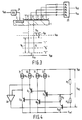
- Fig. 1 shows diagrammatically a CCD having a conventional input stage.
- the device comprises a silicon substrate having a p-type region 1 adjoining the surface 2.
- the input stage comprises an n-type surface zone 3 provided with a connection 4 for applying voltages.
- a series of electrodes 5-9 is arranged, which are insulated from the surface 2 by a thin dielectric layer not shown.
- the electrode 6, designated hereinafter as memory gate, is the gate below which an information-representing charge packet is formed.
- the electrode 5 with clock ⁇ s between the zone 3 and the memory gate 6 constitutes a circuit by means of which the connection between the zone 3 and the memory region below the gate 6 can be closed or interrupted.
- the zone 3 and the electrodes 5,6 together constitute the input stage of the charge-coupled device. Only an adjoining part of the charge transport channel with the electrodes 7,8 and 9 is shown.
- the device constitutes, by way of example, a 4-phase system with the clock voltages ⁇ 1, ⁇ 2, ⁇ 3 and ⁇ 4, the clock ⁇ also being applied for the sake of simplicity to the gate 6.
- the output is also shown diagrammatically with an output gate 10, which is applied to a direct voltage, and an adjoining n-type output zone 11.
- the zone 11 is connected to one of the inputs of the differential amplifier 12, which is shown in the Figure only diagrammatically by a block.
- a reference signal is applied to the input 13 of the amplifier 12 and the output signal derived from the zone 11 is compared with this reference signal.
- the read-out signal can be derived at the output 14 of the amplifier 12.
- the clock voltages ⁇ s and ⁇ 1, ⁇ 2, ⁇ 3 and ⁇ 4 are derived directly from the supply voltage and vary, for example, between 0 V and +5 V.
- the gate 10 is applied to a suitably chosen level between 0 V and 5 V, for example 1.5 V.
- Fig. 1 shows the potential variation in the input stage during the formation of a charge packet (logic "1").
- the (positive) potential is plotted in downward direction. If a voltage which is exactly 5 V is applied to the memory gate 6, a potential well, whose depth is indicated by a full line, is induced below the gate 6.
- the potential level below the switching gate is indicated by the line 16a at a voltage of 5 V and by the level 16b at a reverse voltage of 0 V.
- the potential level of the zone 3 is adjusted to the reference level 17.
- the size of the charge packet now becomes Qo+ ⁇ Q, where ⁇ Q is about 0.1 Qo. If the voltage applied is 4.5 V instead of the nominal voltage of 5 V, the bottom of the (empty) potential well 15 rises to the level 20b. The potential well then becomes less deep and can therefore contain less charge. In order to avoid that overflow of charge from one bit to another bit occurs in the period between writing and reading, the reference level 17 will be chosen so that also the largest charge packet (clock voltage 5.5 V) fits into a shallow potential well (clock voltage 4.5 V).
- Fig. 2a shows the circuit diagram of a 1 MOST/BIT memory cell.
- the information is stored in the memory capacitance C and is supplied or read via the bit line BL.
- the cell is selected by means of the MOS transistor 22, whose gate is connected to the word line WL.
- Fig. 2b shows diagrammatically a cross-section of a possible embodiment of this cell.
- the semiconductor body 1 again comprises a p-type region 1 provided with an n-type surface zone 3, which is connected to the bit line BL.
- the memory capacitance C is constituted by the gate electrode or memory gate 6 and the underlying surface region of the body 1, which is separated by a thin oxide layer from the gate 6.
- the supply voltage of 5 V is applied to the gate 6, as a result of which a potential well is induced in the semiconductor body.
- This potential well 15 is shown in Fig. 2 below the semiconductor body 1.
- the depth of the well fluctuates with the supply voltage, which is indicated by the broken lines.
- the voltage of 5 V is also applied to the gate 5 between the zone 3 and the memory gate 6.
- the signal to be written is applied via the bit line BL to the zone 3.
- the voltage level of the zone 3 is again chosen so that a charge packet, which is formed when the supply voltage is 5.5 V, will not overflow when the voltage at the gate 6 then falls to 4.5 V. With such a choice of the voltage applied to the zone 3, the size of the charge packet will still strongly vary with the supply voltage, which has similar disadvantages as described above for CCD's.
- Fig. 3 shows diagrammatically a charge-coupled device according to the invention, in which this disadvantage is abviated at least to a considerable extent.
- the same reference numerals as in Fig. 1 are used for corresponding components.
- To the clock electrodes 5,6,7,8 etc. are applied clock voltages ⁇ s , ⁇ 1, ⁇ 2, ⁇ 3, ⁇ 4, which are supplied by the clock voltage source 25 and which vary between V ss (for example 0 V or earth) and the voltage V dd (nominal value, for example, 5 V).
- V dd nominal value, for example, 5 V
- To the input diode 3 is applied a voltage V d , which is derived via a reference voltage source 26 from V dd .
- the voltage V d is such that the difference V dd -V d is at least practically independent of fluctuations at V dd , that is to say that V d is subjected to at least practically the same fluctuations as V dd , as a result of which the quantity of charge stored below the gate 6 is practically independent of the fluctuations at V dd .
- the reference voltage source 26 is constituted by a so-called band gap reference, which is well known in the literature and is frequently used in cases in which a low temperature coefficient is desired.
- Reference numeral 15 again designates the potential well below the gate 6.
- the level V ss represents the earth potential.
- the surface potential below the gates 5 and 7 which are applied to earth exceeds by V th the earth potential.
- the drawing also shows the potential level V dd .
- the surface potential below the gate 6 exceeds by V th the level V dd . It is assumed that the threshold voltages below the gates 5,6,7 and 8 have equal values.
- Fig. 4 shows an embodiment which is described in Netherlands Patent Application entitled “Band gap reference circuit", which was filed on 19 February 1988 under Application No. 8800422 in the name of the Applicant and whose contents are incorporated by reference in the present Application.
- the circuit comprises an operational differential amplifier 30, whose output is fed back through the transistor Q10 and through two cascade circuits comprising Q7 and Q9 and Q6 and Q8, respectively, to the two inputs.
- the positive input + is connected to the emitter of the transistor Q7, while the negative input - of the amplifier 30 is connected to the emitter of the transistor Q6.
- the base of Q7 is connected to the emitter of Q9 and the base of Q6 is connected to the emitter of the transistor Q8.
- the base of the transistor Q9 is connected to the junction point P of the voltage divider R10-R11 and through the resistor R9 to the emitter of the transistor Q10 and the base of the transistor Q8.
- the emitters of the transistors Q6 and Q8 are each connected to a current source 31, which supplies a current 5 Io; the emitters of the transistors Q7 and Q9 are each connected to the current source 32, which supplies a current Io.
- the collectors of the transistors are connected to the substrate, which is in turn connected, for example, to earth.
- the operational amplifier 30 supplies such an output signal that the voltage between the input terminals is practically 0 V, that is to say that the emitters of Q6 and Q7 practically have the same potential.
- V bg (V BE10 + jV T 1n 45) (1+R11/R10) + (jV T 1n 45) R11/R9.
- V bg (V BE10 + jV T 1n 45 + V os ) (1+R11/R10) + (jV T 1n 45 + V os ) R11/R9.
- j was chosen to be equal to 2.
- R11/R10 for V bg each value above a minimum value of 1.28 V can be obtained and therefore also the desired value of 2.8 V.
- the circuit shown in Fig. 4 may be constructed together with the charge-coupled device according to CMOS technology or a combined bipolar CMOS technology.
- the differential amplifier 30 and the current sources 31, 32 may be constituted by MOS transistors.
- the bipolar pnp transistors Qi may be constituted by vertical transistors arranged in an N well, the p-type substrate constituting a common collector.
- the output of the band gap reference voltage source of Fig. 4 is connected to a voltage divider 8R-R-4R, which divides the voltage V BG into units 1/13 V BG .
- the junction point between 4R and R is connected to the gate electrode of the n-channel MOST N1.
- the junction point between 8R and R is connected to the gate electrode of the c-channel MOST N2.
- the transistors N1 and N2 are connected to current sources in such a manner that a 4 times larger current flows through N2 than through N1.
- the output voltage is derived at the output terminal 37.
- the transistors N1,N2 are assumed to have the same threshold voltage V th as the charge-coupled device.
- V g1 V CCD - 9 13 V bg (6)
- V g 1 13 V bg (7)
- the principle described here for CCD's may also advantageously be used in a so-called 1 MOST'BIT memory or DRAM, as shown diagrammatically in Fig. 6.
- the supply voltage V dd 5 V is applied to the memory gate 6, as a result of which the potential well 15 is induced in the semiconductor body.
- the input diode 3 may be connected, for example, by means of the "write enable" signal to the reference voltage source 26, which supplies a fixed reference voltage with respect to V dd .
- the voltage level V d is such that, when writing a logic "1", the quantity of charge in the well 15 is again independent of fluctuations in the supply. For the value of the "1" signal, similar considerations as described here for CCD's may be applied.
- the invention is not limited to the embodiment described here, but that many further variations are possible for those skilled in the art within the scope of the invention.
- the invention may also be used in buried channel CCD'S or in bucket brigades (BBD's).
- BBD's bucket brigades
- the reference sources described here other reference voltage sources may also be used.
Landscapes
- Engineering & Computer Science (AREA)
- Microelectronics & Electronic Packaging (AREA)
- Computer Hardware Design (AREA)
- Semiconductor Memories (AREA)
- Solid State Image Pick-Up Elements (AREA)
- Non-Volatile Memory (AREA)
- Static Random-Access Memory (AREA)
- Dram (AREA)
- Read Only Memory (AREA)
Claims (7)
- Halbleiterspeicheranordnung mit einer auf einer Fläche (2) eines Halbleiterkörpers (1) liegenden Source-Zone (3), einem neben der Source-Zone liegenden und von der Oberfläche isolierten Speicher-Gate (6), mit dessen Hilfe eine Potentialmulde (15) in dem Halbleiterkörper induziert werden kann, in dem ein Information darstellendes Ladungspaket (19) in Form einer Menge von von der Source-Zone gelieferten Ladungsträgern gespeichert werden kann, und einem zwischen der Source-Zone und dem Speicher-Gate liegenden und von der Oberfläche isolierten Schalt-Gate (5), mit dem die Verbindung zwischen der Source-Zone und der Potentialmulde hergestellt oder unterbrochen werden kann, dadurch gekennzeichnet, daß zwischen dem genannten Speicher-Gate und der genannten Source-Zone Spannungsstabilisierungsmittel (26) vorhanden sind, mit deren Hilfe während des Einbringens von Ladungsträgern in die genannte Potentialmulde der Source-Zone eine solche Spannung zugeführt werden kann, daß die Potentialdifferenz zwischen dem Speicher-Gate und der Source-Zone und damit die Größe des genannten Ladungspaketes mindestens praktisch vollständig unabhängig von Spannungsschwankungen an dem Speicher-Gate sind.
- Halbleiterspeicheranordnung nach Anspruch 1, dadurch gekennzeichnet, daß die Source-Zone, das Schalt-Gate und das Speicher-Gate die Eingangsstufe einer ladungsgekoppelten Anordnung bilden, mit einem Transportkanal, durch den die eingebrachte Information unter dem Einfluß von an eine Reihe von über dem Transportkanal angeordneten Taktelektroden angelegte Taktspannungen an einen Ausgang transportiert werden kann.
- Halbleiterspeicheranordnung nach Anspruch 2, dadurch gekennzeichnet, daß das Schalt-Gate mit einer Signalquelle verbunden ist, von der aus entweder an das Schalt-Gate eine Spannung gelegt wird, bei der beim Einbringen von Information Ladung von der Source-Zone in die Potentialmulde unter dem Schalt-Gate fließen kann, oder an das Schalt-Gate eine Spannung gelegt wird, bei der die Stromzufuhr zu dieser Potentialmulde vollständig blockiert wird.
- Halbleiterspeicheranordnung nach Anspruch 2 oder 3, dadurch gekennzeichnet, daß Mittel vorhanden sind, mit deren Hilfe die an die Reihe von Taktelektroden gelegten Taktspannungspegel ebenfalls an das Schalt-Gate gelegt werden.
- Halbleiterspeicheranordnung nach Anspruch 1, dadurch gekennzeichnet, daß die Source-Zone, das Schalt-Gate und das Speicher-Gate Teil einer dynamischen 1-MOST/Bit-Speicherzelle sind, mit einem Feldeffekttransistor (22) mit isoliertem Gate, für die einer der Hauptelekrodenbereiche von der genannten Source-Zone gebildet wird, die mit einer Bitleitung verbunden ist, während der andere Hauptelektrodenbereich mit dem Oberflächenbereich unter dem Speichertransistor und die Gate-Elektrode mit einer Wortleitung verbunden ist.
- Halbleiterspeicheranordnung nach einem der vorhergehenden Ansprüche, dadurch gekennzeichnet, daß die genannten Spannungsstabitisierungsmittel eine Bandlücken-Referenzspannungsschaltung umfassen, die eine feste Spannung in bezug auf die an das Speicher-Gate angelegte Spannung erzeugt.
- Halbleiterspeicheranordnung nach Anspruch 1, dadurch gekennzeichnet, daß weiterhin Mittel vorhanden sind, mit deren Hilfe die Schwellenspannung des Speicher-Gates zu der von der Bandlücken-Referenzspannungsschaltung erzeugten Spannung addiert wird.
Priority Applications (1)
| Application Number | Priority Date | Filing Date | Title |
|---|---|---|---|
| AT89200807T ATE98043T1 (de) | 1988-04-05 | 1989-03-30 | Halbleiterspeicheranordnung. |
Applications Claiming Priority (2)
| Application Number | Priority Date | Filing Date | Title |
|---|---|---|---|
| NL8800851A NL8800851A (nl) | 1988-04-05 | 1988-04-05 | Halfgeleidergeheugeninrichting. |
| NL8800851 | 1988-04-05 |
Publications (2)
| Publication Number | Publication Date |
|---|---|
| EP0336498A1 EP0336498A1 (de) | 1989-10-11 |
| EP0336498B1 true EP0336498B1 (de) | 1993-12-01 |
Family
ID=19852057
Family Applications (1)
| Application Number | Title | Priority Date | Filing Date |
|---|---|---|---|
| EP89200807A Expired - Lifetime EP0336498B1 (de) | 1988-04-05 | 1989-03-30 | Halbleiterspeicheranordnung |
Country Status (9)
| Country | Link |
|---|---|
| US (1) | US4987558A (de) |
| EP (1) | EP0336498B1 (de) |
| JP (1) | JP2713456B2 (de) |
| KR (1) | KR970008787B1 (de) |
| AT (1) | ATE98043T1 (de) |
| AU (1) | AU618996B2 (de) |
| DE (1) | DE68911010T2 (de) |
| IE (1) | IE65242B1 (de) |
| NL (1) | NL8800851A (de) |
Families Citing this family (4)
| Publication number | Priority date | Publication date | Assignee | Title |
|---|---|---|---|---|
| US5386384A (en) * | 1993-03-09 | 1995-01-31 | California Institute Of Technology | Parallel CCD memory chip and method of matching therewith |
| US5748035A (en) * | 1994-05-27 | 1998-05-05 | Arithmos, Inc. | Channel coupled feedback circuits |
| US5694445A (en) * | 1994-09-22 | 1997-12-02 | Matshushita Electric Industrial Co., Ltd. | Semiconductor device with means for charge recycling |
| FR2826180B1 (fr) * | 2001-06-19 | 2003-09-19 | St Microelectronics Sa | Dispositif semiconducteur integre de memoire de type dram et procede de fabrication correspondant |
Family Cites Families (17)
| Publication number | Priority date | Publication date | Assignee | Title |
|---|---|---|---|---|
| US3831041A (en) * | 1973-05-03 | 1974-08-20 | Bell Telephone Labor Inc | Compensating circuit for semiconductive apparatus |
| US4011471A (en) * | 1975-11-18 | 1977-03-08 | The United States Of America As Represented By The Secretary Of The Air Force | Surface potential stabilizing circuit for charge-coupled devices radiation hardening |
| US4156818A (en) * | 1975-12-23 | 1979-05-29 | International Business Machines Corporation | Operating circuitry for semiconductor charge coupled devices |
| US4118795A (en) * | 1976-08-27 | 1978-10-03 | Texas Instruments Incorporated | Two-phase CCD regenerator - I/O circuits |
| NL7610351A (nl) * | 1976-09-17 | 1978-03-21 | Philips Nv | Ladingsoverdrachtinrichting. |
| JPS6044752B2 (ja) * | 1978-04-24 | 1985-10-05 | 日本電気株式会社 | ダイナミツクメモリ |
| US4357571A (en) * | 1978-09-29 | 1982-11-02 | Siemens Aktiengesellschaft | FET Module with reference source chargeable memory gate |
| JPS5672530A (en) * | 1979-11-19 | 1981-06-16 | Nec Corp | Semiconductor circuit |
| US4317054A (en) * | 1980-02-07 | 1982-02-23 | Mostek Corporation | Bandgap voltage reference employing sub-surface current using a standard CMOS process |
| US4325018A (en) * | 1980-08-14 | 1982-04-13 | Rca Corporation | Temperature-correction network with multiple corrections as for extrapolated band-gap voltage reference circuits |
| DE3108726A1 (de) * | 1981-03-07 | 1982-09-16 | Deutsche Itt Industries Gmbh, 7800 Freiburg | Monolithisch integrierte referenzspannungsquelle |
| JPS5822423A (ja) * | 1981-07-31 | 1983-02-09 | Hitachi Ltd | 基準電圧発生回路 |
| US4574384A (en) * | 1982-08-25 | 1986-03-04 | Hitachi, Ltd. | Signal transfer system using a charge transfer device |
| DE3321556A1 (de) * | 1983-06-15 | 1984-12-20 | Telefunken electronic GmbH, 7100 Heilbronn | Bandgap-schaltung |
| NL8302731A (nl) * | 1983-08-02 | 1985-03-01 | Philips Nv | Halfgeleiderinrichting. |
| JPS6044752A (ja) * | 1983-08-20 | 1985-03-09 | Matsushita Electric Ind Co Ltd | 空気調和機の送風制御方法 |
| NL8600891A (nl) * | 1986-04-09 | 1987-11-02 | Philips Nv | Halfgeleiderinrichting. |
-
1988
- 1988-04-05 NL NL8800851A patent/NL8800851A/nl not_active Application Discontinuation
-
1989
- 1989-03-30 AT AT89200807T patent/ATE98043T1/de not_active IP Right Cessation
- 1989-03-30 EP EP89200807A patent/EP0336498B1/de not_active Expired - Lifetime
- 1989-03-30 DE DE68911010T patent/DE68911010T2/de not_active Expired - Fee Related
- 1989-03-31 US US07/332,686 patent/US4987558A/en not_active Expired - Fee Related
- 1989-04-03 IE IE104689A patent/IE65242B1/en not_active IP Right Cessation
- 1989-04-03 KR KR89004344A patent/KR970008787B1/ko not_active Expired - Fee Related
- 1989-04-03 AU AU32361/89A patent/AU618996B2/en not_active Ceased
- 1989-04-04 JP JP1084135A patent/JP2713456B2/ja not_active Expired - Lifetime
Also Published As
| Publication number | Publication date |
|---|---|
| KR970008787B1 (en) | 1997-05-29 |
| IE891046L (en) | 1989-10-05 |
| JPH0210866A (ja) | 1990-01-16 |
| ATE98043T1 (de) | 1993-12-15 |
| IE65242B1 (en) | 1995-10-04 |
| AU618996B2 (en) | 1992-01-16 |
| NL8800851A (nl) | 1989-11-01 |
| KR890016752A (ko) | 1989-11-30 |
| AU3236189A (en) | 1989-10-12 |
| US4987558A (en) | 1991-01-22 |
| DE68911010T2 (de) | 1994-05-19 |
| EP0336498A1 (de) | 1989-10-11 |
| JP2713456B2 (ja) | 1998-02-16 |
| DE68911010D1 (de) | 1994-01-13 |
Similar Documents
| Publication | Publication Date | Title |
|---|---|---|
| US4169233A (en) | High performance CMOS sense amplifier | |
| US4495693A (en) | Method of integrating MOS devices of double and single gate structure | |
| US5363325A (en) | Dynamic semiconductor memory device having high integration density | |
| US4879690A (en) | Static random access memory with reduced soft error rate | |
| GB2162394A (en) | Mos static ram | |
| US4003034A (en) | Sense amplifier circuit for a random access memory | |
| JPS6388858A (ja) | ラツチアツプ保護回路付き集積回路 | |
| US4259729A (en) | Dynamic memory | |
| US4725875A (en) | Memory cell with diodes providing radiation hardness | |
| US4109284A (en) | Self-scanning photo-sensitive circuits | |
| EP0336498B1 (de) | Halbleiterspeicheranordnung | |
| EP0139196A2 (de) | Halbleiterspeicher mit einem Spannungsverstärker des ladungsgekoppelten Typs | |
| GB1461683A (en) | Information storage apparatus | |
| GB2149250A (en) | Dynamic memory | |
| US4423490A (en) | JFET Dynamic memory | |
| US3876887A (en) | Mos amplifier | |
| JPS59143360A (ja) | ワンデバイス・メモリ・セル | |
| US4272693A (en) | Analysis circuit for a charge coupled device | |
| JPS61224357A (ja) | 電荷転送装置 | |
| US4250568A (en) | Capacitor semiconductor storage circuit | |
| US4280067A (en) | Semiconductor charge transfer device having a decoupling gate for stopping reverse charge flow | |
| US4492973A (en) | MOS Dynamic memory cells and method of fabricating the same | |
| JPS6322069B2 (de) | ||
| US4712123A (en) | Dynamic memory device | |
| KR930002468B1 (ko) | 기준전위배선을 구비한 반도체 집적회로 |
Legal Events
| Date | Code | Title | Description |
|---|---|---|---|
| PUAI | Public reference made under article 153(3) epc to a published international application that has entered the european phase |
Free format text: ORIGINAL CODE: 0009012 |
|
| AK | Designated contracting states |
Kind code of ref document: A1 Designated state(s): AT CH DE ES FR GB IT LI NL |
|
| 17P | Request for examination filed |
Effective date: 19900406 |
|
| 17Q | First examination report despatched |
Effective date: 19930126 |
|
| GRAA | (expected) grant |
Free format text: ORIGINAL CODE: 0009210 |
|
| AK | Designated contracting states |
Kind code of ref document: B1 Designated state(s): AT CH DE ES FR GB IT LI NL |
|
| PG25 | Lapsed in a contracting state [announced via postgrant information from national office to epo] |
Ref country code: NL Effective date: 19931201 Ref country code: LI Effective date: 19931201 Ref country code: ES Free format text: THE PATENT HAS BEEN ANNULLED BY A DECISION OF A NATIONAL AUTHORITY Effective date: 19931201 Ref country code: CH Effective date: 19931201 Ref country code: AT Effective date: 19931201 |
|
| REF | Corresponds to: |
Ref document number: 98043 Country of ref document: AT Date of ref document: 19931215 Kind code of ref document: T |
|
| REF | Corresponds to: |
Ref document number: 68911010 Country of ref document: DE Date of ref document: 19940113 |
|
| ITF | It: translation for a ep patent filed | ||
| ET | Fr: translation filed | ||
| REG | Reference to a national code |
Ref country code: CH Ref legal event code: PL |
|
| ITTA | It: last paid annual fee | ||
| NLV1 | Nl: lapsed or annulled due to failure to fulfill the requirements of art. 29p and 29m of the patents act | ||
| PLBE | No opposition filed within time limit |
Free format text: ORIGINAL CODE: 0009261 |
|
| STAA | Information on the status of an ep patent application or granted ep patent |
Free format text: STATUS: NO OPPOSITION FILED WITHIN TIME LIMIT |
|
| 26N | No opposition filed | ||
| ITPR | It: changes in ownership of a european patent |
Owner name: CAMBIO RAGIONE SOCIALE;PHILIPS ELECTRONICS N.V. |
|
| REG | Reference to a national code |
Ref country code: FR Ref legal event code: CD |
|
| REG | Reference to a national code |
Ref country code: FR Ref legal event code: CD |
|
| REG | Reference to a national code |
Ref country code: GB Ref legal event code: IF02 |
|
| PGFP | Annual fee paid to national office [announced via postgrant information from national office to epo] |
Ref country code: FR Payment date: 20020327 Year of fee payment: 14 |
|
| PGFP | Annual fee paid to national office [announced via postgrant information from national office to epo] |
Ref country code: GB Payment date: 20020328 Year of fee payment: 14 |
|
| PGFP | Annual fee paid to national office [announced via postgrant information from national office to epo] |
Ref country code: DE Payment date: 20020523 Year of fee payment: 14 |
|
| PG25 | Lapsed in a contracting state [announced via postgrant information from national office to epo] |
Ref country code: GB Free format text: LAPSE BECAUSE OF NON-PAYMENT OF DUE FEES Effective date: 20030330 |
|
| PG25 | Lapsed in a contracting state [announced via postgrant information from national office to epo] |
Ref country code: DE Free format text: LAPSE BECAUSE OF NON-PAYMENT OF DUE FEES Effective date: 20031001 |
|
| GBPC | Gb: european patent ceased through non-payment of renewal fee |
Effective date: 20030330 |
|
| PG25 | Lapsed in a contracting state [announced via postgrant information from national office to epo] |
Ref country code: FR Free format text: LAPSE BECAUSE OF NON-PAYMENT OF DUE FEES Effective date: 20031127 |
|
| REG | Reference to a national code |
Ref country code: FR Ref legal event code: ST |
|
| PG25 | Lapsed in a contracting state [announced via postgrant information from national office to epo] |
Ref country code: IT Free format text: LAPSE BECAUSE OF NON-PAYMENT OF DUE FEES;WARNING: LAPSES OF ITALIAN PATENTS WITH EFFECTIVE DATE BEFORE 2007 MAY HAVE OCCURRED AT ANY TIME BEFORE 2007. THE CORRECT EFFECTIVE DATE MAY BE DIFFERENT FROM THE ONE RECORDED. Effective date: 20050330 |