EP0336449A2 - Flachbau-Kathodenstrahlröhre - Google Patents
Flachbau-Kathodenstrahlröhre Download PDFInfo
- Publication number
- EP0336449A2 EP0336449A2 EP89106299A EP89106299A EP0336449A2 EP 0336449 A2 EP0336449 A2 EP 0336449A2 EP 89106299 A EP89106299 A EP 89106299A EP 89106299 A EP89106299 A EP 89106299A EP 0336449 A2 EP0336449 A2 EP 0336449A2
- Authority
- EP
- European Patent Office
- Prior art keywords
- deflection
- electrodes
- flat configuration
- ray tube
- cathode ray
- Prior art date
- Legal status (The legal status is an assumption and is not a legal conclusion. Google has not performed a legal analysis and makes no representation as to the accuracy of the status listed.)
- Granted
Links
Images

Classifications
-
- H—ELECTRICITY
- H01—ELECTRIC ELEMENTS
- H01J—ELECTRIC DISCHARGE TUBES OR DISCHARGE LAMPS
- H01J31/00—Cathode ray tubes; Electron beam tubes
- H01J31/08—Cathode ray tubes; Electron beam tubes having a screen on or from which an image or pattern is formed, picked up, converted, or stored
- H01J31/10—Image or pattern display tubes, i.e. having electrical input and optical output; Flying-spot tubes for scanning purposes
- H01J31/12—Image or pattern display tubes, i.e. having electrical input and optical output; Flying-spot tubes for scanning purposes with luminescent screen
- H01J31/123—Flat display tubes
- H01J31/125—Flat display tubes provided with control means permitting the electron beam to reach selected parts of the screen, e.g. digital selection
- H01J31/126—Flat display tubes provided with control means permitting the electron beam to reach selected parts of the screen, e.g. digital selection using line sources
Definitions
- the present invention relates to a flat configuration cathode ray tube for applications such as a color television receiver, computer display terminal, etc.
- the flat configuration cathode ray tube is one type of such an apparatus, for example as described in Japanese patent laid-open Nos. 60-189848 and 60-193242.
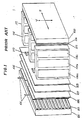
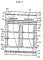
- Fig. 1 is an oblique view of a prior art flat configuration CRT, formed of electrodes which are contained within an external vacuum sealed container, e.g. a glass vacuum vessel
- Fig. 2 is a corresponding partial plan cross-sectional view.
- the horizontal display direction of images or characters displayed by the CRT is indicated by a horizontal arrow H, and the vertical display direction by a vertical arrow V.
- a plurality of mutually separate line cathodes 101, each extending in the vertical direction, are arrayed with a fixed pitch along the horizontal direction.
- the line cathodes 101 are each formed of tungsten wire having a surface coating of a cathode oxide.
- the number of line cathodes 101 and the pitch at which they are arrayed are optional. However assuming for example that the display image size is 10 inches, then the array pitch of the line cathodes 101 would be 10 mm, and 20 line cathodes would be used, each having a vertical height of 160 mm.
- An image display section 102 is separated from the line cathodes 101 by a predetermined spacing.
- Vertical scanning electrodes 103 are disposed behind the line cathodes 101. Each of the vertical scanning electrodes 103 is elongated in the horizontal direction, and the electrodes are arrayed with a fixed pitch in the vertical direction, and supported such as to be mutually electrically isolated upon a supporting member 104.
- the number of the vertical scanning electrodes 103 is 1/n times the total number of horizontal scanning lines of the display, where n is an integer. However in this example it will be assumed that the number of these vertical scanning electrodes 103 is identical to the number of horizontal scanning lines (i.e. if the CRT is to be utilized for a usual television display, approximately 480 lines, for the NTSC standard).
- the line cathodes 101 and the image display section 102 are successively positioned, extending from the line cathodes 101, a set of first grid electrodes (hereinafter abbreviated to G1 electrodes) 105, a second grid electrode (hereinafter abbreviated to G2 electrode) 106, a third grid electrode (hereinafter abbreviated to G3 electrode) 107, and a fourth grid electrode (hereinafter abbreviated to G4 electrode) 108.
- the G1 electrodes 105 each are respectively identical and electrically separate flat-shaped electrodes having respective apertures 109 (shown in Fig. 2) formed therein, with the apertures being positioned in correspondence with respectively ones of the line cathodes 101 as indicated in Fig. 2.
- the G2 to G4 electrodes are each formed as a thin flat plate, with apertures formed therein. Respective video signals are applied to the G1 electrodes 105, for executing electron beam modulation.
- the G2 electrode 106 and the G3 electrode 107 have respective apertures 110 and 111 (shown in Fig. 2) formed therein which are positioned in correspondence with the apertures of the G1 electrodes 105, but are not divided in the vertical direction.
- the G4 electrode 108 has apertures 112 formed therein which may be identical to the apertures 110, 111 of the G2 electrode 106 and G3 electrode 107 respectively, or which may be of greater width in the horizontal direction than in the vertical direction as illustrated in Fig. 1.
- Each of these pairs of horizontal scanning electrodes consists of vertically extending electrodes which are positioned symmetrically with respect to the axis of a corresponding electron beam which is emitted from the line cathodes 101 (as described in detail hereinafter).
- the centers of these pairs of horizontal scanning electrodes are spaced at regular intervals which are identical to the pitch of the line cathodes 101.
- the horizontal deflection electrodes 115A, 115B and 115C are formed by means such as etching of a metallic layer formed by metal plating or evaporative deposition upon surfaces of supporting members 114, each of which is formed of an electrically insulating material. As a result of voltages applied thereto, the horizontal deflection electrodes 115A, 115B and 115C execute horizontal electron beam focusing, electron beam horizontal deflection, and beam acceleration.
- a photo-emissive layer consisting of a screen phosphor layer 116 and a metal back layer electrode 117 is formed on the inner surface of a portion of the glass containing vessel, to thereby constitue an image display section 102.
- the phosphor layer 116 is formed of red (R), green (G) and blue (B) stripes or dots arrayed successively along the horizontal direction, in the case of a colour display.
- This flat configuration CRT is as follows. Heating currents are caused to flow in the line cathodes 101 shown in Fig. 1, which are fixed at a common potential, while a potential that is more negative than that common potential is applied to all of the vertical scanning electrodes 103 other than a currently selected one of the vertical scanning electrodes 103. Respective electron beams, arrayed along a horizontal line corresponding to the selected one of the vertical scanning electrodes 103, are thereby emitted from the vertical scanning electrodes 103, towards the G1 electrodes 105 and the G2 electrode 106.
- a potential which is higher than that of the line cathodes 101 by approximately 100 to 500 V is applied to the G2 electrode 106, causing the electron beams to pass through respective ones of the apertures 110, 111 formed in the G1 electrodes 105 and G2 electrode 106 respectively, after having passed through the apertures 109 of the G1 electrodes 105.
- Control of the level of current of each electron beam is executed by varying the voltage which is applied to the corresponding one of the G1 electrodes 105.
- the electron beams pass through the apertures of the G3 electrode 107 and G4 electrode 108, then pass midway between respective ones of the pairs of mutually opposing sets of horizontal deflection electrodes 115A, 115B and 115C.
- Predetermined voltages are applied to the above electrodes, for causing the electron beams to form respective small spots on the phosphor layer of the image display section 102. Focussing of each beam in the vertical direction is implemented by a static electron lens which is formed at the exit from a corresponding one of the apertures 112 of the G4 electrode 108, while beam focusing in the horizontal direction is implemented by an electron lens formed by the horizontal deflection electrodes.
- Horizontal focus adjustment can be executed by variation of the center values of respective voltages which are applied between each of the opposing pairs of horizontal deflection electrodes 115A, 115B and 115C,
- the horizontal deflection electrodes 115A, 115B and 115C are mutually interconnected by respective pairs of common conductors 115A-a,b 115B-a,b and 115C-a,b.
- a sawtooth waveform deflection voltage or a staircase waveform deflection voltage is applied betwen each of these pairs of common conductors, superimposed upon the respective focus voltages.
- timing control of the modulation signals which are applied to the G1 electrodes 105 can be synchronized with timings at which the electron beams fall upon respective color stripe or dot portions of the phosphor layer 116 of the image display section 102 during each horizontal sweep.
- control of electron emission from the line cathodes 101 is executed by selectively determining the voltages applied to respective ones of the vertical scanning electrodes 103. Specifically, the potential of the space surrounding a line cathode, adjacent to a specific one of the vertical scanning electrodes 103, is is made positive or negative with respect to the potential of the line cathodes 101, in accordance with the voltage applied to that vertical scanning electrode. Electron beam switching for vertical beam scanning is thereby implemented. The smaller the spacing between the line cathodes 101 and the vertical scanning electrodes 103, the smaller will be the level of voltage that is required to control ON/OFF switching of the electron beams emitted from the line cathodes 101.
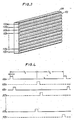
- first vertical scanning interval i.e. a first vertical scanning interval, designated as 1 V A in Fig. 4
- the ON state a condition in which electron beams are generated
- the first horizontal scanning interval i.e. 1 H interval
- a signal is applied to the vertical scanning electrode 103C to establish the electron beam ON state, and thereafter signals are successively applied to the remainder of the odd-numbered vertical scanning electrodes to successively establish the electron beam ON state during sequential 1 H intervals.
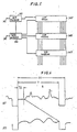
- a timing pulse generator 144 generates timing pulses to be applied to drive circuits that are described hereinafter, in response to a television sync signal 142.
- a corresponding television video signal 141 is converted to successive digital data values by an analog/digital convertor 143, and a set of these data values are sequentially inputted to a line memory 145 during a 1 H interval.
- the data values are then simultaneously transferred to a second line memory 146, and during the succeeding 1 H interval a new set of digital data values are inputted to the line memory 145.
- the data values which have been transferred to the line memory 146 are held therein during a 1 H interval, and are transferred to a digital/analog converter (or pulse-width converter) 147, to be converted to corresponding analog signals (or pulse-width modulated signals). These are amplified, and applied to the G1 electrodes 105 of the CRT.
- the line memories are thereby used to perform time-axis conversion, as can be understood referring to Fig. 6.
- a portion of the input video signal 151 in Fig. 6 that occurs during an interval T within a 1 H interval is divided into A segments, each having a duration of T/A.
- the duration of these signal segments is then multiplied by the factor A, to thereby extend that duration to become equal to T.
- An example of a time-axis expanded signal segment is designated as 152 in Fig. 6. This process is executed for the entirity of each 1 H interval of the input video signal, and as a result of sequential scanning in the vertical direction by the scanning signals applied to the vertical scanning electrodes 103, a complete display image is produced.
- deflection voltages having a periodic waveform such as a sawtooth waveform are applied to the deflection plates for executing horizontal deflection, together with DC voltages superimposed thereon for executing horizontal focusing.
- the levels of these DC voltages are approximately in the range 1 to 20 KV.
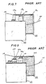
- the horizontal deflection electrodes 115A, 115B and 115C are formed directly upon the supporting members 114, e.g. by etching of a metallic layer formed on the supporting member surface, electrical discharge or insulation breakdown can readily occur in regions between mutually adjacent ones of the horizontal deflection electrodes 115A, 115B and 115C. Structures for such horizontal deflection plates have been proposed in the prior art for overcoming this problem, for example as described in Japanese patent laid-open No. 62-58554.
- Each deflection plate consists of a supporting member 118 formed of an electrically insulating material, with three horizontal deflection electrodes 119a, 119b and 119c mounted thereon (only the electrodes mounted upon one face of each supporting member being shown, for simplicity of description).
- the horizontal deflection electrodes 119a and 119c are formed directly upon a surface of a supporting member 118, as in the preceding prior art example, e.g.
- each of the supporting members 118 has a horizontal deflection electrode 121c formed on a surface thereof in the same way as for electrodes 119c, 119a in Fig. 7.
- each of the horizontal deflection electrodes 121a (or 119a in Fig. 7) is situated at the low-voltage end of the deflection plates, i.e. is subjected to a relatively low DC focusing voltage, while the horizontal deflection electrodes 121c (or 121c in Fig. 8) are situated at the high-voltage end of the deflection plates, and the horizontal deflection electrodes 121b (or 119b in Fig. 7) are positioned intermediate between the high and low voltage ends of the deflection plates.
- a first embodiment of a flat configuration cathode ray tube comprises: a plurality of line cathodes for emission of electrons, successively arrayed with a predetermined pitch; a focus electrode section for focusing respective electron beams which are emitted from the line cathodes; deflection plates having deflection electrodes for executing horizontal deflection of the electron beams after focusing has been executed by the focus electrode section, the deflection electrodes being divided into at least two parts each formed of mutually opposing electrodes; and an image display section upon which the electron beams are incident, for displaying an image; in which the length of a region where deflection is executed by the deflection electrodes, as measured along the trajectory of an electron beam, is within a value which is three times the pitch of the line cathodes.
- a flat configuration cathode ray tube is further characterized in that each of the deflection plates is formed of a supporting member formed of an electrically insulating material, with respective horizontal deflection electrodes mounted thereon, and in that at least a part of the deflection electrodes of each of the deflection plates are mounted on the corresponding electrically insulating material by spacer members, such that at least a portion of mutually adjacent ones of the deflection electrodes mutually overlap by a predetermined amount.
- the deflection electrodes which are thus mounted on spacer members may be formed of metal plates, or of an electrically insulating material such as glass having a metallic film formed thereon.
- a flat configuration cathode ray tube according to the present invention can thereby be made thinner than has been possible in the prior art, while greater reliability and stability of focus operation is ensured due to the suppression of electrical discharge of insulation breakdown between adjacent ones of deflection electrodes which must be utilized, due to space limitations, both for electron beam deflection and for also for focusing the electron beams.
- Fig. 9 is a partial plan cross-sectional view of a first embodiment of a flat configuration CRT according to the present invention. This differs from the prior art in that the distance between the G4 electrode 108 and the image display section 102, i.e.
- the length (measured along the trajectory of an electron beam, assuming that the trajectory is oriented directly perpendicular to the image display section 102) of a region in which horizontal focusing is executed by a set of horizontal deflection plates 113′, is approximately equal to, and no greater than, three times the pitch of the line cathodes 101.
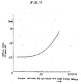
- Fig. 10 shows how the vertical beam focus diameter varies in accordance with changes in the distance between the G4 electrode 108 and the image display section 102.
- the vertical beam focus diameter abruptly deteriorates.
- the spacing pitch of the line cathodes 101 is approximately 15 mm
- this value of 50 mm is approximately three times the pitch of the line cathodes 101. This distance determines the limit of the range of satisfactory focus of each of the vertical focus lenses that are formed by the apertures 112 in the G4 electrode 108.
- the distance from the G4 electrode 108 to the image display section 102 i.e. the length of the horizontal deflection region that is defined by the horizontal deflection plates 113′, no greater than approximately three times the pitch of the line cathodes 101.
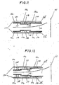
- Fig. 11 is a plan view of a pair of horizontal deflection plates for a second embodiment of a flat configuration cathode ray tube according to the present invention. Only the deflection electrodes on one side of each deflection plate are shown, for simplicity of description. In Fig.
- a pair of deflection plates 113 ⁇ are disposed mutually parallel, each having a set of deflection electrodes 131a, 131b and 131c attached to a supporting member 130 which is formed of an electrically insulating material, with the deflection electrodes 131a, 131b and 131c being positioned at differing heights over the supporting member and attached thereto by a long spacer 132, a short spacer 133, and a long spacer 134 respectively, and with mutually adjacent end portions of the deflection electrodes 131a and 131b and deflection electrodes 131b, 131c respectively mutually overlapping by predetermined amounts.
- each of the deflection electrodes is mounted on spacers, this is not an essential feature, i.e. a part of the deflection electrodes of a deflection plate could be directly mounted on the supporting member 130.
- the respective amounts of overlap need not be identical.
- Each of the supporting members 130 is formed in the shape of a flat plate from an electrically insulating material such as glass.
- the deflection electrodes 131a, 131b and 131c can each be formed of metal plate, or from plates made of an electrically insulating material such as glass having a metal coating formed thereon.
- the deflection electrodes 131a, 131b and 131c are attached to the corresponding supporting member 130 by the spacers 132, 133 and 134, which serve to accurately define the spacing between each deflection electrode and the supporting member 130.
- the spacers are attached to the supporting member 130 by an attachment material 135, such as glass frit.
- Numeral 160 denotes an electron beam
- numeral 161 denotes the inner surface of the image display section upon which the electron beam is incident.
- deflection center voltages respectively supplied to the deflection electrodes 131a, 131b and 131c of each deflection plate would be approximately 0.5 KV, 5 KV and 10 KV.
- the respective deflection electrodes 131a, 131b and 131c of a deflection plate are attached to the supporting member 130 by spacers 132, 133 and 134, the surface distances between the deflection electrodes are made long. Thus it is difficult for surface currents to flow across the spacers 132, 133, 134, and the supporting member 130. Furthermore, due to the fact that the deflection electrodes 131a, 131b and 131c mutually overlap, this serves to prevent the supporting member 130 from becoming electrically charged by the electron beam 160. Moreover, this overlap also has the effect of making the surface distances between the deflection electrodes longer, thereby further reducing the possibility of surface current flow or insulation breakdown occurring in the regions between adjacent horizontal deflection electrodes.
- Deflection plates for a third embodiment of the present invention are illustrated in plan view in Fig. 12. This differs from the second embodiment in that the deflection electrode 131a of each deflection plate is held substantially distant from the supporting member 130 by a long spacer 132′.
- deflection plates of Figs. 11 and 12 have been described for use as horizontal deflection plates, it would also be possible to apply such plates as vertical deflection plates.
- a flat configuration CRT has a plurality of line cathodes (101) arrayed with a predetermined pitch, a focus electrode section for focusing respective electron beams which are emitted from the line cathodes, and pairs of deflection plates (113) having opposed deflection electrodes for executing deflection of the focussed electron beams, the deflection electrodes of each deflection plate being divided into at least two parts (115A, 115B, 115C), and an image display section (102) upon which the electron beams are incident.
- the length of a region in which deflection is executed by the deflection electrodes is made no greater than a value which is approximately three times the pitch of the line cathodes.
Landscapes
- Cathode-Ray Tubes And Fluorescent Screens For Display (AREA)
Applications Claiming Priority (4)
| Application Number | Priority Date | Filing Date | Title |
|---|---|---|---|
| JP87484/88 | 1988-04-08 | ||
| JP63087485A JPH01260745A (ja) | 1988-04-08 | 1988-04-08 | 荷電粒子ビーム偏向板 |
| JP8748488 | 1988-04-08 | ||
| JP87485/88 | 1988-04-08 |
Publications (3)
| Publication Number | Publication Date |
|---|---|
| EP0336449A2 true EP0336449A2 (de) | 1989-10-11 |
| EP0336449A3 EP0336449A3 (de) | 1991-10-02 |
| EP0336449B1 EP0336449B1 (de) | 1995-08-30 |
Family
ID=26428755
Family Applications (1)
| Application Number | Title | Priority Date | Filing Date |
|---|---|---|---|
| EP89106299A Expired - Lifetime EP0336449B1 (de) | 1988-04-08 | 1989-04-10 | Flachbau-Kathodenstrahlröhre |
Country Status (3)
| Country | Link |
|---|---|
| US (1) | US4988913A (de) |
| EP (1) | EP0336449B1 (de) |
| DE (1) | DE68923987T2 (de) |
Families Citing this family (5)
| Publication number | Priority date | Publication date | Assignee | Title |
|---|---|---|---|---|
| AU665006B2 (en) | 1991-07-17 | 1995-12-14 | Canon Kabushiki Kaisha | Image-forming device |
| EP0658916B1 (de) * | 1993-11-09 | 1998-04-15 | Canon Kabushiki Kaisha | Bildanzeigegerät |
| KR100312690B1 (ko) * | 1999-08-25 | 2001-11-03 | 김순택 | 형광표시관 |
| RU2196372C2 (ru) * | 2000-12-25 | 2003-01-10 | Общество с ограниченной ответственностью "ВОЛГА-СВЕТ" | Низковольтный катодолюминесцентный экран |
| RU2479064C2 (ru) * | 2011-05-25 | 2013-04-10 | ОБЩЕСТВО С ОГРАНИЧЕННОЙ ОТВЕТСТВЕННОСТЬЮ "Волга-Свет" (ООО "Волга-Свет") | Источник света |
Family Cites Families (7)
| Publication number | Priority date | Publication date | Assignee | Title |
|---|---|---|---|---|
| JPS60189848A (ja) * | 1984-03-09 | 1985-09-27 | Matsushita Electric Ind Co Ltd | 平板型陰極線管 |
| JPS60193242A (ja) * | 1984-03-14 | 1985-10-01 | Matsushita Electric Ind Co Ltd | 平板形陰極線管 |
| US4703231A (en) * | 1984-06-26 | 1987-10-27 | Matsushita Electric Industrial Co., Ltd. | Flat type image display tube and display device using the same |
| US4752721A (en) * | 1984-09-12 | 1988-06-21 | Matsushita Electric Industrial Co., Ltd. | Charged particle beam deflector and flat CRT using the same |
| JPH07114119B2 (ja) * | 1985-09-09 | 1995-12-06 | 松下電器産業株式会社 | 平板形陰極線管 |
| US4736139A (en) * | 1984-11-19 | 1988-04-05 | Matsushita Electric Industrial Co., Ltd. | Flat type cathode ray tube and color image display apparatus utilizing same |
| US4804887A (en) * | 1986-11-19 | 1989-02-14 | Matsushita Electrical Industrial Co., Ltd. | Display device with vibration-preventing plate for line cathodes |
-
1989
- 1989-04-07 US US07/334,517 patent/US4988913A/en not_active Expired - Lifetime
- 1989-04-10 EP EP89106299A patent/EP0336449B1/de not_active Expired - Lifetime
- 1989-04-10 DE DE68923987T patent/DE68923987T2/de not_active Expired - Fee Related
Also Published As
| Publication number | Publication date |
|---|---|
| EP0336449A3 (de) | 1991-10-02 |
| DE68923987D1 (de) | 1995-10-05 |
| DE68923987T2 (de) | 1996-05-23 |
| EP0336449B1 (de) | 1995-08-30 |
| US4988913A (en) | 1991-01-29 |
Similar Documents
| Publication | Publication Date | Title |
|---|---|---|
| EP0404022B1 (de) | Flache Bildwiedergabevorrichtung und Verfahren zur Herstellung derselben | |
| EP0045350B1 (de) | Bildanzeigevorrichtung | |
| US4804887A (en) | Display device with vibration-preventing plate for line cathodes | |
| US4694225A (en) | Method of driving a flat type of cathode ray tube to provide uniformity of electron beam emission characteristics for a plurality of beam sources | |
| GB2124017A (en) | A deflection colour selection system for a single beam channel plate display tube | |
| EP0328079B1 (de) | Flache Bildwiedergabevorrichtung mit Kathodenstrahlröhre | |
| EP0336449B1 (de) | Flachbau-Kathodenstrahlröhre | |
| US5068579A (en) | Flat configuration color crt display apparatus with scanning correction for component positioning error | |
| EP0271926B1 (de) | Bildwiedergabevorrichtung mit einer flachen Kathodenstrahlröhre | |
| EP0334438A2 (de) | Flache Kathodenstrahlröhren-Bildwiedergabevorrichtung | |
| US5061880A (en) | Method of driving image display device | |
| JP2563282B2 (ja) | 平板形陰極線管 | |
| JPS63193441A (ja) | 平板形陰極線管 | |
| JPS63261661A (ja) | 画像表示装置 | |
| JPS62143347A (ja) | 画像表示装置 | |
| US4137485A (en) | Image display block scanning method | |
| JPS63266740A (ja) | 平板形陰極線管 | |
| JPS61230239A (ja) | 平板形映像管 | |
| JPH07114119B2 (ja) | 平板形陰極線管 | |
| JPS61230240A (ja) | 表示管 | |
| JPS63102143A (ja) | 電子ビ−ム偏向板 | |
| JPS61230249A (ja) | 平板形陰極線管 | |
| JPH0290444A (ja) | 平板形画像表示装置 | |
| JPS63275281A (ja) | 平板形陰極線管の駆動方法 | |
| JPS62211832A (ja) | 平板型陰極線管 |
Legal Events
| Date | Code | Title | Description |
|---|---|---|---|
| PUAI | Public reference made under article 153(3) epc to a published international application that has entered the european phase |
Free format text: ORIGINAL CODE: 0009012 |
|
| 17P | Request for examination filed |
Effective date: 19890410 |
|
| AK | Designated contracting states |
Kind code of ref document: A2 Designated state(s): DE FR GB |
|
| PUAL | Search report despatched |
Free format text: ORIGINAL CODE: 0009013 |
|
| AK | Designated contracting states |
Kind code of ref document: A3 Designated state(s): DE FR GB |
|
| 17Q | First examination report despatched |
Effective date: 19931014 |
|
| GRAA | (expected) grant |
Free format text: ORIGINAL CODE: 0009210 |
|
| AK | Designated contracting states |
Kind code of ref document: B1 Designated state(s): DE FR GB |
|
| PG25 | Lapsed in a contracting state [announced via postgrant information from national office to epo] |
Ref country code: FR Free format text: THE PATENT HAS BEEN ANNULLED BY A DECISION OF A NATIONAL AUTHORITY Effective date: 19950830 |
|
| REF | Corresponds to: |
Ref document number: 68923987 Country of ref document: DE Date of ref document: 19951005 |
|
| EN | Fr: translation not filed | ||
| PLBE | No opposition filed within time limit |
Free format text: ORIGINAL CODE: 0009261 |
|
| STAA | Information on the status of an ep patent application or granted ep patent |
Free format text: STATUS: NO OPPOSITION FILED WITHIN TIME LIMIT |
|
| 26N | No opposition filed | ||
| PG25 | Lapsed in a contracting state [announced via postgrant information from national office to epo] |
Ref country code: DE Effective date: 19970101 |
|
| PGFP | Annual fee paid to national office [announced via postgrant information from national office to epo] |
Ref country code: GB Payment date: 19970401 Year of fee payment: 9 |
|
| PG25 | Lapsed in a contracting state [announced via postgrant information from national office to epo] |
Ref country code: GB Free format text: LAPSE BECAUSE OF NON-PAYMENT OF DUE FEES Effective date: 19980410 |
|
| GBPC | Gb: european patent ceased through non-payment of renewal fee |
Effective date: 19980410 |