EP0335660B1 - Wärmebeständiges, isolierendes Substrat, thermischer Druckkopf und thermografischer Apparat - Google Patents
Wärmebeständiges, isolierendes Substrat, thermischer Druckkopf und thermografischer Apparat Download PDFInfo
- Publication number
- EP0335660B1 EP0335660B1 EP89303052A EP89303052A EP0335660B1 EP 0335660 B1 EP0335660 B1 EP 0335660B1 EP 89303052 A EP89303052 A EP 89303052A EP 89303052 A EP89303052 A EP 89303052A EP 0335660 B1 EP0335660 B1 EP 0335660B1
- Authority
- EP
- European Patent Office
- Prior art keywords
- heat
- layer
- resistant
- resin
- printing head
- Prior art date
- Legal status (The legal status is an assumption and is not a legal conclusion. Google has not performed a legal analysis and makes no representation as to the accuracy of the status listed.)
- Revoked
Links
Images

Classifications
-
- H—ELECTRICITY
- H10—SEMICONDUCTOR DEVICES; ELECTRIC SOLID-STATE DEVICES NOT OTHERWISE PROVIDED FOR
- H10W—GENERIC PACKAGES, INTERCONNECTIONS, CONNECTORS OR OTHER CONSTRUCTIONAL DETAILS OF DEVICES COVERED BY CLASS H10
- H10W70/00—Package substrates; Interposers; Redistribution layers [RDL]
- H10W70/60—Insulating or insulated package substrates; Interposers; Redistribution layers
- H10W70/67—Insulating or insulated package substrates; Interposers; Redistribution layers characterised by their insulating layers or insulating parts
- H10W70/69—Insulating materials thereof
- H10W70/695—Organic materials
-
- B—PERFORMING OPERATIONS; TRANSPORTING
- B41—PRINTING; LINING MACHINES; TYPEWRITERS; STAMPS
- B41J—TYPEWRITERS; SELECTIVE PRINTING MECHANISMS, i.e. MECHANISMS PRINTING OTHERWISE THAN FROM A FORME; CORRECTION OF TYPOGRAPHICAL ERRORS
- B41J2/00—Typewriters or selective printing mechanisms characterised by the printing or marking process for which they are designed
- B41J2/315—Typewriters or selective printing mechanisms characterised by the printing or marking process for which they are designed characterised by selective application of heat to a heat sensitive printing or impression-transfer material
- B41J2/32—Typewriters or selective printing mechanisms characterised by the printing or marking process for which they are designed characterised by selective application of heat to a heat sensitive printing or impression-transfer material using thermal heads
- B41J2/335—Structure of thermal heads
- B41J2/33505—Constructional details
- B41J2/3353—Protective layers
-
- B—PERFORMING OPERATIONS; TRANSPORTING
- B41—PRINTING; LINING MACHINES; TYPEWRITERS; STAMPS
- B41J—TYPEWRITERS; SELECTIVE PRINTING MECHANISMS, i.e. MECHANISMS PRINTING OTHERWISE THAN FROM A FORME; CORRECTION OF TYPOGRAPHICAL ERRORS
- B41J2/00—Typewriters or selective printing mechanisms characterised by the printing or marking process for which they are designed
- B41J2/315—Typewriters or selective printing mechanisms characterised by the printing or marking process for which they are designed characterised by selective application of heat to a heat sensitive printing or impression-transfer material
- B41J2/32—Typewriters or selective printing mechanisms characterised by the printing or marking process for which they are designed characterised by selective application of heat to a heat sensitive printing or impression-transfer material using thermal heads
- B41J2/335—Structure of thermal heads
- B41J2/3355—Structure of thermal heads characterised by materials
-
- B—PERFORMING OPERATIONS; TRANSPORTING
- B41—PRINTING; LINING MACHINES; TYPEWRITERS; STAMPS
- B41J—TYPEWRITERS; SELECTIVE PRINTING MECHANISMS, i.e. MECHANISMS PRINTING OTHERWISE THAN FROM A FORME; CORRECTION OF TYPOGRAPHICAL ERRORS
- B41J2/00—Typewriters or selective printing mechanisms characterised by the printing or marking process for which they are designed
- B41J2/315—Typewriters or selective printing mechanisms characterised by the printing or marking process for which they are designed characterised by selective application of heat to a heat sensitive printing or impression-transfer material
- B41J2/32—Typewriters or selective printing mechanisms characterised by the printing or marking process for which they are designed characterised by selective application of heat to a heat sensitive printing or impression-transfer material using thermal heads
- B41J2/335—Structure of thermal heads
- B41J2/3359—Manufacturing processes
Definitions
- thermographic apparatus such as facsimile or printer
- thermal printing head to be used therein
- heat-resistant electrically insulating substrate to be used in the thermal printing head and various electronic devices.
- heat-resistant insulating substrates having insulating layers or heat-accumulating layers of such heat-resistant resin as a polyimide resin on substrates of a varying kind have been finding growing utility as high-resistance base plates for thermal printing heads and as supporting base plates for various electronic devices such as hybrid IC grade multilayer circuit boards which are required to exhibit performance of high reliability in spite of effects of heat.
- the conventional high-resistance base plates produced by forming a glazed glass layer as an insulating layer capable of controlling radiation and accumulation of heat on a substrate of such a ceramic substance as alumina are giving place to heat-resistant resin layer such as a polyimide resin layer on ceramic substrates or metallic substrates.
- One thermal printing head provided with this polyimide resin layer as an insulating layer is known to possess the following construction, for example.
- the thermal printing head is produced by superposing a heat-resistant resin layer formed of a polyimide resin, for example, and intended to serve concurrently as a heat-accumulating layer and a heat-resistant layer on a metallic substrate made of a Fe alloy, for example, covering the heat-resistant resin layer with a heat-generating resistor film such as of Ta-SiO2 or Ti-SiO2 by the sputtering technique, further depositing on the heat-generating resistor film such several electrodes and common electrodes made of Al or Al-Si Cu, for example, and adapted to give rise to openings destined to serve as heat-generating parts, and forming an abrasion-resistant layer of silicon oxynitride (Si-O-N), for example, in such a manner as to cover at least the heat-generating parts and serve concurrently as an antioxidant film (hereinafter referred to as "abrasion-resistant layer," the term "abrasion-resistant layer" as used in the present specification and the appended claims shall be construed as
- the thermal printing head of this construction owing to the use of the insulating layer of polyimide resin which possesses a heat diffusion ratio as low as one third to one sixth of that of the conventional glazed glass layer, is pre-eminently excellent in thermal efficiency. Further, since this thermal printing head is allowed to use the metallic substrate, namely a supporting substrate possessing flexibility, it can tolerate the impacts of the bending work. It is, therefore, attracting attention as a compact and inexpensive thermal head of high performance. This thermal printing head, however, encounters the following problem during the course of its manufacture.
- the heat-resistant resin layer sustains an injury.
- the polyimide resin layer is suffered to emit a gas abundantly. This gas brings about an adverse effect of rendering the control of the magnitude of resistance difficult. Further, during the distribution of wires by the wire bonding technique, the elasticity of the polyimide resin layer renders the work of bonding difficult.
- the present applicant for patent formerly proposed a thermal head having interposed between the heat-resistant resin layer and the heat-generating resistor layer a resin-protecting layer made of such an inorganic insulating substance as alumina, silicon oxynitride, or Sialon (Si-Al-ON) (Japanese Patent Application Disclosure SHO 63 (1988)-189,253, SHO 63(1988)-297,066, and Japanese Patent Application SHO 62(1987)-191,655).
- the polyimide resin layer is prevented from sustaining an injury and the polyimide resin layer from emitting gas during the manufacture of the thermal printing head and the thermal printing head is allowed to acquire certain improvement in rigidity.
- the produced thermal printing head has an effect of enabling the actual work of mounting to be carried out stably.
- This superposition of the resin-protecting layer on the heat-resistant resin layer constitutes itself an effective measure for enabling the actual work of mounting to be stably performed because this resin-protecting layer serves not merely as a high-resistance base plate for a thermal head but also as an insulating substrate for other electronic devices.
- Japanese Patent Application Disclosure SHO 61(1986)-297,159 discloses a thermal printing head which comprises a ceramic substrate, a glazed glass layer covering the ceramic substrate, a layer of a compound, i.e. silicon nitride doped with a stated amount of oxygen, superposed on the glazed glass layer, and a heat-generating resistor layer further superposed on the doped compound layer.
- This compound layer precludes diffusion of a defiling substance from the glazed glass layer to the heat-generating resistor layer and protects the glazed glass layer against fusion.
- Japanese Patent Application Disclosure SHO 62(1987)-117,760 discloses a thermal printing head comprising a glazed glass layer, a polyimide resin layer formed on the glazed glass layer, and an adhesive layer of such an inorganic substance as NiCr, Cr, or Ti and an insulating layer formed of SiO2, Si-O-N4, or Al2O3 both superposed on the polyimide resin layer to ensure adhesiveness to the polyimide resin layer and materialize an insulating heat-resistant layer.
- This construction permits a reduction in the power applied to the thermal printing head.
- the heat-resistant insulating substrate comprising a layer of such a heat-resistant resin as polyimide resin and a resin-protecting layer of such an inorganic insulating substance as alumina, silicon oxynitride, or Sialon (Si-Al-ON) superposed on the heat-resistant resin layer
- a high-resistance base member for a thermal printing head for example, there are derived various advantages.
- the inorganic insulator layer mentioned above does not acquire any sufficient film strength but entails the following problem.
- This phenomenon may be logically explained by a postulate that in the thermal printing head which uses the high-resistance base member incorporating therein a glazed glass layer or a glass layer as an insulating layer, the substrate in its entirety possesses high rigidity enough to be prevented from yielding to local deformation and sustaining the crack of the nature mentioned above because the abrasion-resistant layer, on exposure to local pressure, is only suffered to deform in the same pattern as the substrate.
- the resin-protecting layer enhances the rigidity of the substrate to a certain extent
- the capacity of the layer of the resin for deformation is conspicuous as compared with the abrasion-resistant layer.
- the deformation of the heat-resistant layer cannot be prevented by the resin-protecting layer and the abrasion-resistant layer. It is consequently though that the crack occurs when the deformation of the resin-protecting layer or the abrasion-resistant layer fails to follow the deformation of the heat-resistant resin layer.
- the problem of this nature is not limited to the thermal printing head.
- the deformation sustained by the heat-resistant resin layer as during the course of actual mounting inflicts breakage of wire in the wire-distribution layer and eventually impairs the outcome of the bonding work.
- An object of this invention is to provide a heat-resistant insulating substrate possessing high rigidity.
- Another object of this invention is to provide a heat-resistant insulating substrate adapted to repress the ratio of occurrence of defectives during the course of actual mounting.
- a further object of this invention is to provide a thermal heat such that, when it is set in place in a printer, for example, the abrasion-resistant layer used therein absolutely no crack or only sparing crack.
- Still another object of this invention is to provide a thermal printing head capable of producing a stable printing operation.
- Yet another object of this invention is to provide a thermal printing head prevented from sustaining an injury in the heat-resistant resin layer thereof during the course of manufacture, enabled to effect easy control of the magnitude of resistance, and allowed to yield to stable wire bonding during the work of actual mounting.
- a further object of this invention is to provide a thermal printing head enabled to acquire enhanced strength without requiring any increase in the thickness of the abrasion-resistant layer.
- thermographic apparatus capable of effecting a stable printing operation.
- thermographic apparatus capable of highly reliable operation.
- a first aspect of the present invention provides a heat-resistant electrically insulating substrate, comprising a highly thermoconductive supporting substrate and a heat-resistant resin layer formed on the supporting substrate, characterised in that a resin-protecting layer is deposited on the heat-resistant resin layer and formed of one layer, or a plurality of layers, of an amorphous substance including hydrogen and/or halogen and having as main components thereof silicon and at least one member selected from nitrogen, carbon and oxygen.
- a second aspect of the present invention provides a thermal printing head as set out in claim 3.
- thermographic apparatus as set out in claim 5.
- the heat-resistant resin layer to be used in the heat-resistant insulating substrate, the thermal printing head, and the thermographic apparatus of this invention is desired to be formed of one layer, or a plurality of layers, of polyimide resin, polyamide resin, polyamideimide resin, or a mixture of the resins.
- it is made of the polyimide resin.
- the resin-protecting layer or the abrasion-resistant layer or both which is formed of one layer, or a plurality of layers, of an amorphous substance containing at least one member from among hydrogen and halogen elements and using as main components thereof silicon and at least one member selected from among nitrogen, carbon, and oxygen is produced by any of the conventional methods such as, for example, sputtering method, ion-plating method, vacuum deposition method, plasma CVD method, ECR plasma CVD method, thermal CVD method, and photo-CVD method.
- the plasma CVD method proves to be particularly advantageous in respect that the produced film enjoys fast adhesiveness, the treatment can be carried out at a relatively low temperature without impairing the characteristics of the substrate, and the physical properties, i.e. electrical properties and optical properties, of the film can be controlled easily.
- the substrate to be covered is formed of a heat-resistant resin, the temperature of the substrate is not allowed, even when polyimide resin is employed as the heat-resistant resin, to exceed 550°C, a temperature tolerated thermally by the polyimide resin in an ordinary run.
- the method employed for the production mentioned above must be capable of permitting the treatment to be carried out at a temperature lower than the tolerable temperature mentioned above.
- the plasma CVD method which uses the raw material gases including SiH4 gas and SiF4 gas as Si components and N2 gas, CH4 gas, and N2O gas as other components forms a thin ceramic film aimed at on the substrate by converting the raw material gases into a plasma in a vacuum and allowing the plasma to deposit on the substrate.
- the film occludes such halogen elements as hydrogen and fluorine from the raw material gases.
- the produced thin film is capable of retaining its amorphous state stably owing to the effects of such occluded elements.
- the resin-protecting layer or the abrasion-resistant layer in the thermal printing head or as the resin-protecting layer in the heat-resistant insulating substrate respectively of the present invention there is formed a layer of an amorphous substance containing at least one member from among hydrogen and halogen elements and using as main components thereof silicon and at least one member selected from among nitrogen, carbon, and oxygen.
- this layer of amorphous substance contains hydrogen and halogen elements and abounds in transition, the layer as a film possesses high toughness. Since the layer is formed of an inorganic substance unlike polyimide, the substrate itself exhibits an appreciably high hardness.
- the substrate as a whole or the thermal head as a whole possesses high rigidity and high crackproofness.
- it is enabled to preclude the crack which would otherwise be inflicted owing to local deformation of the heat-resistant layer of polyimide resin under the pressure exerted on the surface layer.
- the prevention of the heat-resistant resin layer in the thermal printing head from deformation is considered alone, it could be accomplished by increasing the thickness of the abrasion-resistant layer. Since this measure enlarges the distance between the heat-generating resistor and the thermosensitive paper, it not only entails serious drawbacks of quality such as impairment of efficiency and impairment of resolving power but also degrades the capacity for mass production in a large measure.
- the substrate as a whole is allowed to acquire high strength without requiring any increase in the thickness of the layer.
- the heat-resistant insulating substrate of this invention is enabled by the improvement of hardness of the resin-protecting layer to enhance the stability of the work of mounting and curb the ratio of occurrence of defects due to breakage of wire.
- this heat-resistant insulating substrate is used as a high-resistance base plate in the thermal printing head, it goes to stabilizing the printing operation of the thermal printing head.
- the thermal printing head of this invention prevents the heat-resistant resin layer from sustaining an injury during the course of manufacture thereof, facilitates the control of the magnitude of resistance, enables the operation of wire bonding to be carried out stably during the work of actual mounting, effectively prevents the abrasion-resistant layer as a surface layer from sustaining a crack during the actual printing operation, and therefore enables the printing to proceed stably and enjoys decided improvement in reliability of operation.
- thermographic apparatus of this invention enjoys a remarkable improvement in the reliability of performance.
- Fig. 1 is a perspective view illustrating in a partially disassembled state a typical thermal printing head as one embodiment of this invention.
- Fig. 2 is a flow chart of the process of production of the thermal printing head as one embodiment of this invention.
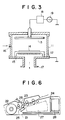
- Fig. 3 is a diagram illustrating the construction of a plasma CVD device used in the formation of a layer of amorphous substance in a working example of this invention.
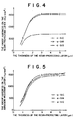
- Fig. 4 is a graph showing the relation between the thickness of the resin-protecting layer and the Knoop hardness in the working example of this invention.
- Fig. 5 is a graph showing the relation between the thickness of the resin-protecting layer and the knoop hardness thereof on the abrasion-resistant layer in the working example of this invention.
- Fig. 6 is a model diagram illustrating in a cross section the thermographic apparatus of this invention.
- Fig. 1 is a structural diagram of the essential part of a typical thermal printing head as one embodiment of this invention.
- 1 stands for a metallic substrate made of a Fe-Cr alloy, for example, in a thickness of about 0.5 mm.
- a heat-resistant resin layer 2 formed of one layer, or a plurality of layers, of polyimide resin or polyamideimide resin or a mixture thereof and destined to serve concurrently as a heat-accumulating layer and an insulating layer is superposed in a thickness of about 20 ⁇ m.
- a resin-protecting layer 3 made of an amorphous substance using as main components thereof silicon and at least one member from among nitrogen, carbon, and oxygen and containing at least one member from among hydrogen and halogen elements is formed in a thickness in the range of 1 to 10 ⁇ m.
- the layers mentioned above jointly form a heat-resistant insulating substrate 4.
- a heat-generating resistor member 5 made of Ta-SiO2, for example is formed on the heat-resistant insulating substrate 4.
- several electrodes 6 and a common electrode 7 formed of Al or Al-Si-Cu, for example, in a thickness approximately in the range of 0.7 to 1 um in such a manner as to give rise to openings destined to serve as heat-generating parts 10 are superposed.
- an adhesive layer 8 made of SiO2 and an abrasion-resistant layer 9 made of Si-O-N and adapted to serve additionally as an antioxidant layer are formed so as to cover at least the openings intended to serve as heat-generating parts 10 are formed.
- This thermal printing head when pulses of voltage spaced by pertinent time intervals are applied between the several electrodes 6 and the common electrode 7, the heat-generating resistor members corresponding to the openings destined to serve as heat-generating parts 10 generate heat to effect printing and recording.
- This thermal printing head is manufactured as follows, for example.
- the metallic substrate 1 of a Fe-Cr alloy having a Fe content of 16 wt% is cut in a prescribed size, degreased, washed, dried, and heat-treated at a temperature in the range of 600°C to 800°C in an atmosphere of dry hydrogen (Fig. 2-a).
- polyimide varnish or polyamideimide varnish is spread with a roll coater or a spin coater in an amount calculated to form a film 20 to 30 ⁇ m in thickness after firing.
- the applied layer of the varnish is dried and fired to give rise to the heat-resistant resin layer 2 (Fig. 2-b).
- the heat-resistant insulating substrate 4 is completed by forming the resin-protecting layer 3, following the procedure described hereinbelow and using a parallel-plate capacitive coupling type plasma CVD device illustrated in Fig. 3.
- the raw material gas is introduced through a gas inlet 16 into the vacuum chamber 11 and discharged through an outlet 17 in such a manner as to maintain the interior of the vacuum chamber 11 to a vacuum degree approximately in the range of 0.05 to 1.0 Torr and, at the same time, the electric power from a high-frequency power source 19 is advanced via a matching box 18 to the high-frequency electrode 13, with the result that glow discharge occurs between the electrodes to convert the raw material gas into a plasma and give rise to a thin film aimed at on the treating substrate 14.
- the plasma CVD method produces a film at a very high rate as shown in Table 1.
- a film of a heat-generating resistor substance such as Ta-SiO2 or Ti-SiO2 is deposited by the sputtering method or other known method (Fig. 2-e) and a film of an electrode substance such as Al, Al-Si-Cu, or Au is formed by the sputtering method (Fig. 2-f).
- a masking film is formed in a desired circuit pattern so as to give rise to openings destined to serve as heat-generating parts.
- several heat-generating resistor members 5, several electrodes 6, and a common electrode 7 are formed by a chemical dry etching treatment, for example (Fig. 2-g).
- the thermal printing head is completed by forming an adhesive layer 8 of SiO2 and an abrasion-resistant layer 9 of Si-O-N by the sputtering method or other method (Fig. 2-h).
- an a-SiN film, an a-SiC film, and an a-SiO film were severally superposed as the resin-protecting layer 3, each in varying thicknesses of 50 nm, 1 ⁇ m, 2 ⁇ m, 3 ⁇ m, and 5 ⁇ m by the procedure described above.
- the films thus formed were tested for Knoop hardness.
- the thickness of the resin-protecting layer is desired to be approximately in the range of 1 to 10 ⁇ m.
- the thermal printing heads provided severally with a-SiN films, and a-SiO films of the varying thickness mentioned above were mounted on radiating substrates of Al with a double-face adhesive tape and subjected to a wire-distribution test by the ultrasonic bonding with the driving IC's similarly mounted on driver substrates. Consequently, they were found to permit stable bonding.
- the thermal printing heads obtained as described above were left standing for 1,000 hours in a constant temperature consant humidity bath at 60 C and 90% RH, they remained perfectly intact and sustained no crack.
- thermal printing heads were each set in a printer and put to trial printing operation. This printing was performed at normal room temperature under normal pressure. After a 5-km running test, the thermal printing head using an a-SiN film 50 nm in thickness as the resin-protecting layer sustained cracks at five places in the abrasion-resistant layer and the thermal heads using an a-SiC film and an a-SiO film each 50 nm in thickness as the resin-protecting layer sustained cracks at eight places, whereas the thermal printing heads using an a-SiN film, an a-SiC film, and an a-SiO film each 1 ⁇ m, 2 ⁇ m, 3 ⁇ m, and 5 ⁇ m in thickness were found to sustain virtually no discernible crack.
- thermo printing head identical in construction with the thermal printing head of the present embodiment was manufactured, excepting a Sialon layer 1 um in thickness was formed by the sputtering method as the resin-protecting layer. After a 5-km running test, this thermal printing head sustained cracks at 20 places in the abrasion-resistant layer.
- the a-SiN film, the a-SiC film, or the a-SiO film to be formed by the plasma CVD method as the resin-protecting layer between the heat-resistant resin layer and the heat-generating resistor prevents the heat-resistant resin layer from sustaining an injury when the electrode substance and the heat-generating resistor substance are melted and removed in a desired circuit pattern and also prevents the heat-generating resistor substance from emitting a gas during its formation in a vacuum.
- the thermal printing head permits stabilization of the magnitude of resistance.
- the wire bonding operation during the course of actual mounting of the thermal printing head can be carried out stably because the cushioning effect manifested by the heat-resistant resin layer can be offset by the hardness of the resin-protecting layer.
- the a-SiN film, the a-SiC film, or the a-SiO film in the present embodiment possesses very high hardness as compared with the heat-resistant resin layer and is not required to have a very large thickness. Even when local pressure is exerted on the abrasion resistant layer during the actual printing operation, the resin-protecting layer prevents the heat-resistant resin layer from deformation. It, therefore, precludes local deformation and protects the abrasion-resistant layer against crack. As the result, the thermal head is enabled to continue its printing operation stably for a long time and enjoy very high reliability of operation.
- the working examples have been described as ones using a-SiN film, a-SiC film, a-SiO film, a-SiCN film, a-SiON film, and a-SiCO film severally as the resin-protecting layer.
- a plurality of these films may be jointly used in a superposed state as the resin-protecting layer to produce the same effect.
- an a-SiN film or an a-SiO film advantageous in terms of film-forming speed was formed in a thickness of about 3 ⁇ m on the heat-resistant resin layer and an a-SiC film advantageous in terms of resistance to etching (chemical dry etching) was superposed in a thickness of about 0.3 ⁇ m.
- a laminated resin-protecting layer composed of an a-SiO film possessing a high film-forming speed as a first layer and an a-SiC film excelling in resistance to etching as a second layer proved to be advantageous from the practical point of view. To be specific, it permitted a decrease in the time required for the process of manufacture and excelled in productivity.
- the a-SiC film forming the second layer comes into direct contact with the resistor film and, therefore, is required to possess an electrically insulating property. It fulfils its part safely so long as it exhibits specific resistivity of not less than 1011 ⁇ cm.
- a two-layer laminate may be formed by superposing two a-SiC films differing in carbon concentration, with the film of lower carbon concentration disposed on the heat-resistant resin layer side to heighten the film-forming speed and the film of higher carbon concentration on the resistor film side to enhance the resistance to etching.
- the hardness and the resistance to crack both are heightened in proportion as the total concentration of oxygen, nitrogen, and carbon contained in the films of a-SiO, a-SiN, a-SiC, a-SiON, a-SiOC, and a-SiNC is increased.
- the laminated layer discharges its role safely so long as the total concentration exceeds 10 atomic percent. Where the resistance to etching is taken into consideration, the total concentration is desired to be not less than 20%.
- the characteristics of the heat-resistant insulating substrate have been evaluated with respect to the performance as a thermal printing head.
- the thermal head is not the only embodiment of the heat-resistant insulating substrate contemplated by the present invention.
- the substrate of this invention may be embodied in a hybrid IC quality multilayer circuit board, for example.
- the stability of the work of mounting can be ensured and the occurrence of defects due to fracture of the wire distribution layer can be effectively prevented by the ability of the resin-protecting layer to enhance hardness.
- the heat-resistant insulating substrate manifests its numerous effects to great advantage.
- thermo printing head using an a-SiN film, an a-SiC film, or an a-SiO film, for example, as an abrasion-resistant layer will be described below as another embodiment of the heat-resistant insulating substrate.
- polyimide resin was deposited as a heat-resistant resin layer on the metallic substrate prepared as described in the preceding embodiment and SiO2 was superposed by the sputtering method in a thickness of 1 ⁇ m as a resin-protecting layer on the heat-resistant resin layer, to complete a heat-resistant insulating substrate.
- heat-resistant insulating substrate heat-generating resistor members, several electrodes, and a common electrode were formed by following the same procedure, and an a-SiN film, an a-SiC film, or an a-SiO film was formed thereon by the plasma CVD method as an abrasion-resistant layer, to complete a thermal printing head.
- the abrasion-resistant layer was given a varying thickness of 2 ⁇ m, 3 ⁇ m, 5 ⁇ m, and 8 ⁇ m.
- a thermal printing head provided with an abrasion-resistant layer of Ta2O5 deposited by the sputtering method and a thermal printing head provided with an abrasion-resistant layer of Si-O-N deposited by the sputtering method using a target composed of Si3N4 and 25% by weight of SiO2 were prepared.
- the thermal printing heads were each set in place in a printer and put to 5-km printing test. During the test, count was taken of the number of cracks sustained in the abrasion-resistant layers of the thermal printing head. The results are shown in Table 2.
- Table 2 Material for abrasion-resistant layer The Number of cracks sustained by abrasion-resistant layer 2 ⁇ m 3 ⁇ m 5 ⁇ m 8 ⁇ m
- Example of this invention a-SiN film 2 0 0 0 a-SiC film 1 0 0 0 a-SiO film 5 1 0 0
- the abrasion-resistant layer is desired to have a thickness of not less than 3 ⁇ m.
- the resin-protecting layer is given still higher hardness, for example, the abrasion-resistant layer having a thickness of about 2 ⁇ m fulfils its role satisfactorily.
- the thickness of the abrasion-resistant layer is unduly large, the efficiency of the thermal printing head is impaired.
- the thickness therefore, is desired not to exceed 8 ⁇ m.
- the a-SiN film, the a-SiC film, the a-SiO film, the a-SiCN film, the a-SiON film, or the a-SiCO film formed by the plasma CVD method and used as an abrasion-resistant layer is prevented from sustaining a crack during the actual printing operation.
- the thermal printing head using this abrasion-resistant layer therefore, enjoys high quality.
- the film obtained by the plasma CVD method contains hydrogen and halogen elements and abounds with transitions, it excels the conventional Ta2O5 film and Si-O-N film in terms of toughness.
- each of the embodiments described above has been depicted as having a heat-resistant resin layer formed on a metallic substrate.
- the material of the supporting substrate is not limited to metal.
- the effect of the present invention can be expected to be similarly obtained even when the material is a ceramic substance or glass.
- the metallic substrate is employed as a supporting substrate, however, it contributes in a large measure to miniaturization of the thermal printing head because the metallic substrate itself can be used as a common electrode and also because it can be bent at will.
- the resin-protecting layer of this invention may be formed by the sputtering method using a target composed of silicon and at least one member from among nitrogen, oxygen, and carbon in an atmosphere of gas containing hydrogen or a halogen element.
- thermographic apparatus i.e. one form of the thermographic apparatus
- Fig. 6 is a model diagram of the facsimile as one embodiment of the present invention.
- thermosensitive recording paper 22 is conveyed by a platen roller 23 and a pair of driving rollers 26 and, at the same time, the platen roller 23 is urged toward the thermal printing head 21 side to hold down the thermosensitive recording paper 22.
- the printing is accomplished by causing a recording signal forwarded from a data processing circuit 24 to a thermal printing head 21 to be processed with a driving element 25 installed on the thermal printing head 21, feeding electric pulses to dots necessary for the printing thereby heating the dots and consequently inducing discoloration of the corresponding parts of the thermosensitive recording paper 22.
- An optical part 27 is a device for reading letters and figures on a given paper desired to be transmitted with an optical device and converting them into electric signals.
- a power source part 28 is a device for supplying electric power to set the component parts of the facsimile into operation.
- the thermal head since the thermal head has a heat-resistant resin layer formed on a metallic substrate, it possesses thermal efficiency about 1.8 times as high as that of the conventional thermal printing head and warrants a generous saving in power consumption.
- the electric energy which the thermal printing head requires in producing prints of a fixed density is about 40% lower than that required by the conventional thermal printing head.
Landscapes
- Engineering & Computer Science (AREA)
- Manufacturing & Machinery (AREA)
- Electronic Switches (AREA)
Claims (6)
- Wärmebeständiges, elektrisch isolierendes Substrat, mit einem gut wärmeleitenden Trägersubstrat (1) und einer wärmebeständigen Harzschicht (2), die auf dem Trägersubstrat gebildet ist, dadurch gekennzeichnet, daß auf die wärmebeständige Harzschicht (2) eine harzschützende Schicht (3) aufgebracht ist, die aus einer Schicht oder einer Vielzahl von Schichten einer amorphen Substanz besteht, die Wasserstoff und/oder Halogen umfaßt, und als Hauptkomponenten Silizium und mindestens eines der Elemente Stickstoff, Kohlenstoff und Sauerstoff enthält.
- Warmebeständiges, elektrisch isolierendes Substrat gemäß Anspruch 1, dadurch gekennzeichnet, daß die wärmebeständige Harzschicht (2) Polyimid oder Polyamidimid als Hauptkomponente enthält.
- Thermischer Druckkopf, mit einem gut wärmeleitenden Trägersubstrat (1), einer wärmebeständigen Harzschicht (2), die auf dem Trägersubstrat (1) gebildet ist, einer harzschützenden Schicht (3), die auf die wärmebeständige Harzschicht (2) aufgebracht ist, einer Vielzahl von wärmeerzeugenden Widerstandselementen (5), die auf der harzschützenden Schicht (3) gebildet sind, wobei diese wärmeerzeugenden Widerstandselemente (5) wärmeerzeugende Teile (10) haben, Leitern (6,7), die an die wärmeerzeugenden Widerstandselemente (5) angeschlossen sind, und einer abriebfesten Schicht (9), die so angeordnet ist, daß sie mindestens die wärmeerzeugenden Teile (10) der wärmeerzeugenden Widerstandselemente (5) bedeckt, wobei die harzschützende Schicht (3) und/oder die abriebfeste Schicht (9) aus einer Schicht oder einer Vielzahl von Schichten einer amorphen Substanz bestehen, die Wasserstoff und/oder Halogen umfaßt, und als Hauptkomponenten Silizium und mindestens eines der Elemente Stickstoff, Kohlenstoff und Sauerstoff enthält.
- Thermischer Druckkopf gemäß Anspruch 3, dadurch gekennzeichnet, daß die wärmebeständige Harzschicht (2) Polyimid oder Polyamidimid als Hauptkomponente enthält.
- Thermografischer Apparat, mit wärmeempfindlichem Aufzeichnungspapier (22), Transportmitteln (23,26), um das wärmeempfindliche Aufzeichnungspapier zu transportieren, einem thermischen Druckkopf (21), um Ausdrucke auf dem wärmeempfindlichen Aufzeichnungspapier (22) zu erzeugen, Ansteuerelementen (25) zum Ansteuern der wärmeerzeugenden Widerstände (5) des thermischen Druckkopfes (21) entsprechend den Aufzeichnungssignal-Daten, und einer Datenverarbeitungsschaltung (24), um Aufzeichnungssignale für die Ansteuerelemente (25) zu erzeugen, wobei der thermische Druckkopf (21) aufweist: ein gut wärmeleitendes Trägersubstrat (1), eine wärmebeständige Harzschicht (2), die auf dem Trägersubstrat (1) gebildet ist, und eine harzschützende Schicht (3), die auf der wärmebeständigen Harzschicht (2) gebildet ist, eine Vielzahl von wärmeerzeugenden Widerständen (5), die auf der harzschützenden Schicht (3) gebildet sind, wobei diese wärmeerzeugenden Widerstände (5) wärmeerzeugende Teile (10) haben, Leiter (6,7), die an die wärmeerzeugenden Widerstände (5) angeschlossen sind, und eine abriebfeste Schicht (9), die so angeordnet ist, daß mindestens die wärmeerzeugenden Teile (10) der wärmeerzeugenden Widerstände (5) bedeckt sind, wobei die harzschützende Schicht (3) und/oder die abriebfeste Schicht (9) aus einer Schicht oder aus einer Vielzahl von Schichten einer amorphen Substanz bestehen, die Wasserstoff und/oder Halogen umfaßt, und als Hauptkomponenten Silizium und mindestens eines der Elemente Stickstoff, Kohlenstoff und Sauerstoff enthält.
- Thermografischer Apparat gemäß Anspruch 5, dadurch gekennzeichnet, daß die wärmebeständige Harzschicht (2) des thermischen Druckkopfes (21) Polyimid oder Polyamidimid als Hauptkomponente enthält.
Applications Claiming Priority (4)
| Application Number | Priority Date | Filing Date | Title |
|---|---|---|---|
| JP74241/88 | 1988-03-28 | ||
| JP7424188 | 1988-03-28 | ||
| JP63227524A JPH021339A (ja) | 1988-03-28 | 1988-09-13 | 耐熱性絶縁基板、サーマルヘッドおよび感熱記録装置 |
| JP227524/88 | 1988-09-13 |
Publications (3)
| Publication Number | Publication Date |
|---|---|
| EP0335660A2 EP0335660A2 (de) | 1989-10-04 |
| EP0335660A3 EP0335660A3 (en) | 1990-05-02 |
| EP0335660B1 true EP0335660B1 (de) | 1993-09-01 |
Family
ID=26415358
Family Applications (1)
| Application Number | Title | Priority Date | Filing Date |
|---|---|---|---|
| EP89303052A Revoked EP0335660B1 (de) | 1988-03-28 | 1989-03-28 | Wärmebeständiges, isolierendes Substrat, thermischer Druckkopf und thermografischer Apparat |
Country Status (3)
| Country | Link |
|---|---|
| US (3) | US4963893A (de) |
| EP (1) | EP0335660B1 (de) |
| DE (1) | DE68908749T2 (de) |
Families Citing this family (5)
| Publication number | Priority date | Publication date | Assignee | Title |
|---|---|---|---|---|
| JPH03205165A (ja) * | 1989-08-28 | 1991-09-06 | Ricoh Co Ltd | サーマルヘッド |
| JP3115453B2 (ja) * | 1992-12-28 | 2000-12-04 | 三菱電機株式会社 | サーマルヘッドおよび感熱記録装置 |
| JP3069247B2 (ja) * | 1994-07-29 | 2000-07-24 | アルプス電気株式会社 | サーマルヘッド |
| JPH10129021A (ja) * | 1996-10-25 | 1998-05-19 | Fuji Photo Film Co Ltd | 感熱記録システム |
| EP1226951A3 (de) * | 2001-01-29 | 2003-03-12 | Alps Electric Co., Ltd. | Energiesparthermokopf |
Citations (1)
| Publication number | Priority date | Publication date | Assignee | Title |
|---|---|---|---|---|
| JPS62117760A (ja) * | 1985-11-19 | 1987-05-29 | Fujitsu Ltd | サ−マルヘツド |
Family Cites Families (13)
| Publication number | Priority date | Publication date | Assignee | Title |
|---|---|---|---|---|
| JPS58118273A (ja) * | 1982-01-06 | 1983-07-14 | Hitachi Ltd | 感熱記録ヘツド |
| JPS5993366A (ja) * | 1982-11-19 | 1984-05-29 | Hitachi Ltd | サ−マルヘツド |
| JPS61167574A (ja) * | 1985-01-21 | 1986-07-29 | Nippon Telegr & Teleph Corp <Ntt> | サ−マルヘツド及びその製造方法 |
| US4768038A (en) * | 1985-05-17 | 1988-08-30 | Konishiroku Photo Industry Co., Ltd. | Thermal printhead integrated circuit device |
| US4772496A (en) * | 1985-06-15 | 1988-09-20 | Showa Denko Kabushiki Kaisha | Molded product having printed circuit board |
| JPS6221428A (ja) * | 1985-07-19 | 1987-01-29 | Toyo Seikan Kaisha Ltd | 深絞り成形容器の製法 |
| JPS6277476A (ja) * | 1985-10-01 | 1987-04-09 | Tdk Corp | 保護膜及びその製造法 |
| US4777103A (en) * | 1985-10-30 | 1988-10-11 | Fujitsu Limited | Electrophotographic multi-layered photosensitive member having a top protective layer of hydrogenated amorphous silicon carbide and method for fabricating the same |
| JPH0712786B2 (ja) * | 1985-12-05 | 1995-02-15 | マツダ株式会社 | 自動車のドア構造 |
| JPS62191655A (ja) * | 1986-02-18 | 1987-08-22 | Ngk Spark Plug Co Ltd | 超音波燃料霧化装置 |
| EP0251036B1 (de) * | 1986-06-25 | 1991-05-08 | Kabushiki Kaisha Toshiba | Wärmekopf |
| KR930004777B1 (ko) * | 1987-01-31 | 1993-06-08 | 가부시키가이샤 도시바 | 내열성 절연피복재 및 이것을 이용한 써말 헤드 |
| US5435212A (en) * | 1992-10-30 | 1995-07-25 | Eaton Corporation | Semi-automatic shift implementation |
-
1989
- 1989-03-27 US US07/328,980 patent/US4963893A/en not_active Expired - Lifetime
- 1989-03-28 DE DE89303052T patent/DE68908749T2/de not_active Revoked
- 1989-03-28 EP EP89303052A patent/EP0335660B1/de not_active Revoked
-
1990
- 1990-05-04 US US07/519,179 patent/US5119112A/en not_active Expired - Lifetime
-
1991
- 1991-12-09 US US07/804,014 patent/US5177498A/en not_active Expired - Lifetime
Patent Citations (1)
| Publication number | Priority date | Publication date | Assignee | Title |
|---|---|---|---|---|
| JPS62117760A (ja) * | 1985-11-19 | 1987-05-29 | Fujitsu Ltd | サ−マルヘツド |
Also Published As
| Publication number | Publication date |
|---|---|
| EP0335660A2 (de) | 1989-10-04 |
| US5119112A (en) | 1992-06-02 |
| EP0335660A3 (en) | 1990-05-02 |
| DE68908749T2 (de) | 1994-02-10 |
| DE68908749D1 (de) | 1993-10-07 |
| US4963893A (en) | 1990-10-16 |
| US5177498A (en) | 1993-01-05 |
Similar Documents
| Publication | Publication Date | Title |
|---|---|---|
| US6375312B1 (en) | HEAT GENERATING RESISTOR CONTAINING TaN0.8, SUBSTRATE PROVIDED WITH SAID HEAT GENERATING RESISTOR FOR LIQUID JET HEAD, LIQUID JET HEAD PROVIDED WITH SAID SUBSTRATE, AND LIQUID JET APPARATUS PROVIDED WITH SAID LIQUID JET HEAD | |
| US6080970A (en) | Wafer heating apparatus | |
| EP1014399B1 (de) | Flexibler Dünnfilmkondensator und Herstellungsverfahren | |
| JPH07280462A (ja) | 均熱セラミックスヒーター | |
| WO2001038600A1 (en) | Articles coated with aluminum nitride by chemical vapor deposition | |
| EP0355998A1 (de) | Glaskeramisches Substrat mit einer elektrisch leitenden Schicht | |
| US5177498A (en) | Heat-resistant insulating substrate, thermal printing head, and thermographic apparatus | |
| US5276423A (en) | Circuit units, substrates therefor and method of making | |
| EP0202877A2 (de) | Integrierte Schaltungsanordnung und Verfahren zu deren Herstellung | |
| US20030060146A1 (en) | Thermal head lapping apparatus | |
| JPS5846079B2 (ja) | 多層配線板の製造方法 | |
| KR20020029093A (ko) | 스퍼터링 프로세스 | |
| US4786916A (en) | Thermal head | |
| US20060098052A1 (en) | Thermal Head, Method Of Manufacturing The Same, And Thermal Printer | |
| JPH048554A (ja) | 耐熱性絶縁基板及びサーマルヘッド | |
| KR920005317B1 (ko) | 내열성 절연기판, 서멀헤드 및 감열 기록 장치 | |
| JPH0278576A (ja) | 耐熱性絶縁基板およびサーマルヘッド | |
| JPH0278575A (ja) | 耐熱性絶縁基板およびサーマルヘッド | |
| JPH0278574A (ja) | 耐熱性絶縁基板およびサーマルヘッド | |
| EP0459481B1 (de) | Herstellungsverfahren eines Thermodruckkopfes | |
| JP2000177158A (ja) | サーマルヘッドおよびその製造方法 | |
| US4985712A (en) | Thermal head | |
| JPH0278573A (ja) | 耐熱性絶縁基板およびサーマルヘッド | |
| JP3367995B2 (ja) | 複層セラミックスヒーター | |
| US6115055A (en) | Thermal head |
Legal Events
| Date | Code | Title | Description |
|---|---|---|---|
| PUAI | Public reference made under article 153(3) epc to a published international application that has entered the european phase |
Free format text: ORIGINAL CODE: 0009012 |
|
| 17P | Request for examination filed |
Effective date: 19890412 |
|
| AK | Designated contracting states |
Kind code of ref document: A2 Designated state(s): DE FR GB |
|
| PUAL | Search report despatched |
Free format text: ORIGINAL CODE: 0009013 |
|
| AK | Designated contracting states |
Kind code of ref document: A3 Designated state(s): DE FR GB |
|
| 17Q | First examination report despatched |
Effective date: 19911029 |
|
| GRAA | (expected) grant |
Free format text: ORIGINAL CODE: 0009210 |
|
| AK | Designated contracting states |
Kind code of ref document: B1 Designated state(s): DE FR GB |
|
| REF | Corresponds to: |
Ref document number: 68908749 Country of ref document: DE Date of ref document: 19931007 |
|
| ET | Fr: translation filed | ||
| PLBI | Opposition filed |
Free format text: ORIGINAL CODE: 0009260 |
|
| 26 | Opposition filed |
Opponent name: HI-TEC ELECTRONIK VERTRIEBS GMBH Effective date: 19940601 |
|
| PGFP | Annual fee paid to national office [announced via postgrant information from national office to epo] |
Ref country code: FR Payment date: 19960126 Year of fee payment: 8 |
|
| PGFP | Annual fee paid to national office [announced via postgrant information from national office to epo] |
Ref country code: GB Payment date: 19960319 Year of fee payment: 8 |
|
| PGFP | Annual fee paid to national office [announced via postgrant information from national office to epo] |
Ref country code: DE Payment date: 19960328 Year of fee payment: 8 |
|
| RDAG | Patent revoked |
Free format text: ORIGINAL CODE: 0009271 |
|
| STAA | Information on the status of an ep patent application or granted ep patent |
Free format text: STATUS: PATENT REVOKED |
|
| GBPR | Gb: patent revoked under art. 102 of the ep convention designating the uk as contracting state |
Free format text: 960206 |
|
| 27W | Patent revoked |
Effective date: 19960206 |