EP0459481B1 - Herstellungsverfahren eines Thermodruckkopfes - Google Patents
Herstellungsverfahren eines Thermodruckkopfes Download PDFInfo
- Publication number
- EP0459481B1 EP0459481B1 EP19910108862 EP91108862A EP0459481B1 EP 0459481 B1 EP0459481 B1 EP 0459481B1 EP 19910108862 EP19910108862 EP 19910108862 EP 91108862 A EP91108862 A EP 91108862A EP 0459481 B1 EP0459481 B1 EP 0459481B1
- Authority
- EP
- European Patent Office
- Prior art keywords
- layer
- substrate
- heat resistant
- resin layer
- resistant resin
- Prior art date
- Legal status (The legal status is an assumption and is not a legal conclusion. Google has not performed a legal analysis and makes no representation as to the accuracy of the status listed.)
- Expired - Lifetime
Links
- 238000004519 manufacturing process Methods 0.000 title claims description 7
- 239000000758 substrate Substances 0.000 claims description 61
- 229920006015 heat resistant resin Polymers 0.000 claims description 43
- 229920005989 resin Polymers 0.000 claims description 43
- 239000011347 resin Substances 0.000 claims description 43
- 229910052751 metal Inorganic materials 0.000 claims description 30
- 239000002184 metal Substances 0.000 claims description 30
- 238000000034 method Methods 0.000 claims description 27
- 229920001721 polyimide Polymers 0.000 claims description 27
- 239000004642 Polyimide Substances 0.000 claims description 25
- 238000006552 photochemical reaction Methods 0.000 claims description 11
- 239000000919 ceramic Substances 0.000 claims description 7
- 239000004593 Epoxy Substances 0.000 claims description 4
- 239000004952 Polyamide Substances 0.000 claims description 2
- 239000004962 Polyamide-imide Substances 0.000 claims description 2
- PNEYBMLMFCGWSK-UHFFFAOYSA-N aluminium oxide Inorganic materials [O-2].[O-2].[O-2].[Al+3].[Al+3] PNEYBMLMFCGWSK-UHFFFAOYSA-N 0.000 claims description 2
- 229910052593 corundum Inorganic materials 0.000 claims description 2
- 229920002647 polyamide Polymers 0.000 claims description 2
- 229920002312 polyamide-imide Polymers 0.000 claims description 2
- 229910001845 yogo sapphire Inorganic materials 0.000 claims description 2
- 239000010410 layer Substances 0.000 description 123
- 238000000059 patterning Methods 0.000 description 11
- 238000010438 heat treatment Methods 0.000 description 10
- VYPSYNLAJGMNEJ-UHFFFAOYSA-N silicon dioxide Inorganic materials O=[Si]=O VYPSYNLAJGMNEJ-UHFFFAOYSA-N 0.000 description 8
- 239000000463 material Substances 0.000 description 7
- 229910052681 coesite Inorganic materials 0.000 description 6
- 229910052906 cristobalite Inorganic materials 0.000 description 6
- 239000000377 silicon dioxide Substances 0.000 description 6
- 229910052682 stishovite Inorganic materials 0.000 description 6
- 229910052905 tridymite Inorganic materials 0.000 description 6
- 239000007789 gas Substances 0.000 description 5
- 229910004012 SiCx Inorganic materials 0.000 description 4
- 229920005575 poly(amic acid) Polymers 0.000 description 4
- 229910052814 silicon oxide Inorganic materials 0.000 description 4
- 238000012360 testing method Methods 0.000 description 4
- KFZMGEQAYNKOFK-UHFFFAOYSA-N Isopropanol Chemical compound CC(C)O KFZMGEQAYNKOFK-UHFFFAOYSA-N 0.000 description 3
- 238000006243 chemical reaction Methods 0.000 description 3
- 230000000694 effects Effects 0.000 description 3
- CBCKQZAAMUWICA-UHFFFAOYSA-N 1,4-phenylenediamine Chemical compound NC1=CC=C(N)C=C1 CBCKQZAAMUWICA-UHFFFAOYSA-N 0.000 description 2
- SECXISVLQFMRJM-UHFFFAOYSA-N N-Methylpyrrolidone Chemical compound CN1CCCC1=O SECXISVLQFMRJM-UHFFFAOYSA-N 0.000 description 2
- -1 Si-Zr-Y-O-N Inorganic materials 0.000 description 2
- 229910002795 Si–Al–O–N Inorganic materials 0.000 description 2
- 229910006360 Si—O—N Inorganic materials 0.000 description 2
- 230000003213 activating effect Effects 0.000 description 2
- 229910052782 aluminium Inorganic materials 0.000 description 2
- 229910052799 carbon Inorganic materials 0.000 description 2
- QDOXWKRWXJOMAK-UHFFFAOYSA-N dichromium trioxide Chemical compound O=[Cr]O[Cr]=O QDOXWKRWXJOMAK-UHFFFAOYSA-N 0.000 description 2
- 239000003960 organic solvent Substances 0.000 description 2
- 239000009719 polyimide resin Substances 0.000 description 2
- 239000002243 precursor Substances 0.000 description 2
- 230000005855 radiation Effects 0.000 description 2
- 239000000243 solution Substances 0.000 description 2
- 239000000126 substance Substances 0.000 description 2
- JVERADGGGBYHNP-UHFFFAOYSA-N 5-phenylbenzene-1,2,3,4-tetracarboxylic acid Chemical compound OC(=O)C1=C(C(O)=O)C(C(=O)O)=CC(C=2C=CC=CC=2)=C1C(O)=O JVERADGGGBYHNP-UHFFFAOYSA-N 0.000 description 1
- IJGRMHOSHXDMSA-UHFFFAOYSA-N Atomic nitrogen Chemical compound N#N IJGRMHOSHXDMSA-UHFFFAOYSA-N 0.000 description 1
- OKTJSMMVPCPJKN-UHFFFAOYSA-N Carbon Chemical compound [C] OKTJSMMVPCPJKN-UHFFFAOYSA-N 0.000 description 1
- LFQSCWFLJHTTHZ-UHFFFAOYSA-N Ethanol Chemical compound CCO LFQSCWFLJHTTHZ-UHFFFAOYSA-N 0.000 description 1
- 229910017060 Fe Cr Inorganic materials 0.000 description 1
- 229910000640 Fe alloy Inorganic materials 0.000 description 1
- 229910002544 Fe-Cr Inorganic materials 0.000 description 1
- 229910018594 Si-Cu Inorganic materials 0.000 description 1
- 229910004205 SiNX Inorganic materials 0.000 description 1
- 229910008465 Si—Cu Inorganic materials 0.000 description 1
- QAOWNCQODCNURD-UHFFFAOYSA-N Sulfuric acid Chemical compound OS(O)(=O)=O QAOWNCQODCNURD-UHFFFAOYSA-N 0.000 description 1
- 229910007733 Zr—O—N Inorganic materials 0.000 description 1
- 238000007259 addition reaction Methods 0.000 description 1
- 239000000853 adhesive Substances 0.000 description 1
- 230000001070 adhesive effect Effects 0.000 description 1
- 230000002411 adverse Effects 0.000 description 1
- 230000004075 alteration Effects 0.000 description 1
- XAGFODPZIPBFFR-UHFFFAOYSA-N aluminium Chemical compound [Al] XAGFODPZIPBFFR-UHFFFAOYSA-N 0.000 description 1
- 239000007864 aqueous solution Substances 0.000 description 1
- 125000003118 aryl group Chemical group 0.000 description 1
- 238000004380 ashing Methods 0.000 description 1
- UPHIPHFJVNKLMR-UHFFFAOYSA-N chromium iron Chemical compound [Cr].[Fe] UPHIPHFJVNKLMR-UHFFFAOYSA-N 0.000 description 1
- 238000004140 cleaning Methods 0.000 description 1
- 238000003776 cleavage reaction Methods 0.000 description 1
- 239000011247 coating layer Substances 0.000 description 1
- 238000007796 conventional method Methods 0.000 description 1
- 238000005520 cutting process Methods 0.000 description 1
- 230000003247 decreasing effect Effects 0.000 description 1
- 239000003599 detergent Substances 0.000 description 1
- 238000010586 diagram Methods 0.000 description 1
- 229910001873 dinitrogen Inorganic materials 0.000 description 1
- 238000010494 dissociation reaction Methods 0.000 description 1
- 230000005593 dissociations Effects 0.000 description 1
- 238000009826 distribution Methods 0.000 description 1
- 238000001312 dry etching Methods 0.000 description 1
- 238000005516 engineering process Methods 0.000 description 1
- 239000003822 epoxy resin Substances 0.000 description 1
- 239000000945 filler Substances 0.000 description 1
- 239000011521 glass Substances 0.000 description 1
- 229910052737 gold Inorganic materials 0.000 description 1
- 230000001678 irradiating effect Effects 0.000 description 1
- 238000012423 maintenance Methods 0.000 description 1
- 230000000873 masking effect Effects 0.000 description 1
- 239000000203 mixture Substances 0.000 description 1
- 239000000178 monomer Substances 0.000 description 1
- 230000007935 neutral effect Effects 0.000 description 1
- 229910052757 nitrogen Inorganic materials 0.000 description 1
- 230000003287 optical effect Effects 0.000 description 1
- 239000011368 organic material Substances 0.000 description 1
- 230000010355 oscillation Effects 0.000 description 1
- 230000001590 oxidative effect Effects 0.000 description 1
- 229910052763 palladium Inorganic materials 0.000 description 1
- 230000035515 penetration Effects 0.000 description 1
- 238000000206 photolithography Methods 0.000 description 1
- 238000005268 plasma chemical vapour deposition Methods 0.000 description 1
- 229910052697 platinum Inorganic materials 0.000 description 1
- 229920000647 polyepoxide Polymers 0.000 description 1
- 238000012545 processing Methods 0.000 description 1
- 239000010453 quartz Substances 0.000 description 1
- 238000007142 ring opening reaction Methods 0.000 description 1
- 230000007017 scission Effects 0.000 description 1
- 238000004544 sputter deposition Methods 0.000 description 1
- 238000006467 substitution reaction Methods 0.000 description 1
- 235000011149 sulphuric acid Nutrition 0.000 description 1
- 238000009834 vaporization Methods 0.000 description 1
- 230000008016 vaporization Effects 0.000 description 1
- XLYOFNOQVPJJNP-UHFFFAOYSA-N water Substances O XLYOFNOQVPJJNP-UHFFFAOYSA-N 0.000 description 1
Images
Classifications
-
- B—PERFORMING OPERATIONS; TRANSPORTING
- B41—PRINTING; LINING MACHINES; TYPEWRITERS; STAMPS
- B41J—TYPEWRITERS; SELECTIVE PRINTING MECHANISMS, i.e. MECHANISMS PRINTING OTHERWISE THAN FROM A FORME; CORRECTION OF TYPOGRAPHICAL ERRORS
- B41J2/00—Typewriters or selective printing mechanisms characterised by the printing or marking process for which they are designed
- B41J2/315—Typewriters or selective printing mechanisms characterised by the printing or marking process for which they are designed characterised by selective application of heat to a heat sensitive printing or impression-transfer material
- B41J2/32—Typewriters or selective printing mechanisms characterised by the printing or marking process for which they are designed characterised by selective application of heat to a heat sensitive printing or impression-transfer material using thermal heads
- B41J2/335—Structure of thermal heads
- B41J2/33555—Structure of thermal heads characterised by type
- B41J2/3357—Surface type resistors
-
- B—PERFORMING OPERATIONS; TRANSPORTING
- B41—PRINTING; LINING MACHINES; TYPEWRITERS; STAMPS
- B41J—TYPEWRITERS; SELECTIVE PRINTING MECHANISMS, i.e. MECHANISMS PRINTING OTHERWISE THAN FROM A FORME; CORRECTION OF TYPOGRAPHICAL ERRORS
- B41J2/00—Typewriters or selective printing mechanisms characterised by the printing or marking process for which they are designed
- B41J2/315—Typewriters or selective printing mechanisms characterised by the printing or marking process for which they are designed characterised by selective application of heat to a heat sensitive printing or impression-transfer material
- B41J2/32—Typewriters or selective printing mechanisms characterised by the printing or marking process for which they are designed characterised by selective application of heat to a heat sensitive printing or impression-transfer material using thermal heads
- B41J2/335—Structure of thermal heads
- B41J2/3359—Manufacturing processes
Definitions
- This invention relates to a method of manufacturing a thermal head having a high resistance substrate comprising a heat resistant resin coating layer as a heat insulating layer.
- thermal head is utilized for various recording apparatuses such as a facsimile, a printer for a word processor, or the like, on account of the advantages of noiseless, no need of in maintenance, a low running cost, etc. It is desirable that these recording apparatuses be compact, inexpensive, and low power consuming. Accordingly, a compact, inexpensive, and high-efficient thermal head has been required.
- the above-described polyimide layer was difficult to use for a thermal head in practice, since it is difficult to obtain a resin which can be used for the polyimide layer 2 serving as a heat insulating layer in the thermal head, i.e., a resin which has such heat resistance and adhesion enough to withstand the operation of the thermal head.
- the present inventors developed aromatic polyimide having the following molecular structure, and opened a prospect for realizing a thermal head having a heat insulating layer made of resin (see USP 4868584).
- the polyimide is formed as follows: a ring-opening poly-addition reaction is performed using a equimolar mixture of a biphenyl tetracarboxylic acid dihydride and a p-phenylene diamine, 0.05 to 10 mol% of p-phenylene diamine being replaced by bisaminosiloxane, to produce a polyamic acid; and the polyamic acid is coated on a metal substrate and baked, thereby forming a polyimide layer on the substrate.
- the polyimide layer not only enables the thermal head to operate at a high efficiency but also provides a high characteristic in image quality. Similar polyimide resins are described in the Summary of SPSE's 5th International Congress on Advances in Non-Impact Printing Technologies, pages 501 - 512 (November 12, 1989).
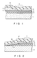
- Fig. 1 is an example of the above-mentioned thermal head.
- the thermal head includes a metal substrate 1, on which a polyimide layer 2 is formed.
- a resin protecting layer 3 is formed on the polyimide layer 2 to protect polyimide from CDE (Chemical Dry Etching) and ashing, to control the resistance of a heat-generating resistive layer (which will be formed later) easily, and to prevent a crack which may be caused by foreign material rolled up by the thermal head having a resin layer serving as a heat insulating layer.
- a heating resistor 4 made of Ta-SiO2, Nb-SiO2 and the like is formed on the resin protecting layer 3.
- An individual electrode 6 and a common electrode 7 made of Al, Al-Si-Cu and the like are formed on the heat-generating resistor so as to form an opening to serve as a heat-generating portion 5. In this manner, the heating portion 5 is formed.
- a protecting layer 8 made of Si-O-N, Si-Al-O-N, Si-Zr-Y-N-O, and the like is formed so as to cover at least the heat-generating portion 5.
- the above-mentioned thermal head which comprises a high-resistance substrate having a metal substrate and a resin layer formed thereon, has the following advantages and is expected to be a high performance thermal head of a next generation.
- One of the methods of patterning a resin on a metal substrate for forming a common electrode using a metal substrate is to print polyamic acid on the metal substrate into a predetermined pattern by a screen printer.
- a filler must be added to polyamic acid to control the thixotropy and the viscosity to obtain a paste suitable for the printing.
- Such a paste cannot provide the above-described advantages of a heat resistant layer made of polyimide.
- an unprinted portion of the metal substrate which should serve as a common electrode may be oxidized by an oxide gas generated during the dehydrating cyclizing reaction, with the result that an insulting layer is formed on that portion.
- Another method of patterning a resin layer is to plate a portion of the metal substrate surface with a metal which is not easily adhesive to polyimide and are not oxidized easily (e.g. Pt, Pd, and Au), coat a resin layer on the substrate using the plated portion, and remove the plated portion.
- a metal which is not easily adhesive to polyimide and are not oxidized easily e.g. Pt, Pd, and Au
- This method requires complicated manufacturing processes and high cost.
- the thermal head as shown in Fig. 1 requires an insulating layer, i.e., a ceramic film serving as a resin protecting layer. Hence, it is also necessary to form a pattern for the ceramic film.
- edges of the pattern form an angle of about 90°C with the substrate.
- step coverage of the thin resistor film and conductive film on the edge is deteriorated to cause disconnection of these films.
- a preferable patterning method for using the metal substrate as a common electrode has been awaited.
- the present invention has been conceived to overcome the above-described problems of the conventional art, and its object is to provide a method of manufacturing a thermal head using a high resistance substrate having a metal substrate and a heat resistant resin layer formed thereon, wherein patterning of the resin layer to form a common electrode using the metal substrate is satisfactorily performed, and the property of the resin layer is fully utilized, thereby improving the quality of the product.
- a method of manufacturing a thermal head comprises the steps of: forming a heat resistant resin layer on a substrate; removing a portion of the heat resistant resin layer by photochemical reaction by means of excimer laser which emits beams having a wavelength of 150 to 400nm, thereby exposing the portion of the substrate; forming a heating resistor layer on the heat resistant resin layer and the exposed portion of the substrate; and forming a conductive film and an individual electrode on the heating resistor layer.
- the property of the resin material is not degraded, and a heat resistant resin layer of a desirable property can be formed.
- the heat resistant resin layer is removed basically by photochemical reaction rather than heat, alteration by heat is prevented.
- the edges of the heat resistant resin layer formed by the laser beams are tapered, sufficient step coverage of the heating resistor layer with the conductive film thereon can be obtained. Hence, the heat resistant resin layer and layers formed thereon are not easily disconnected.
- the thermal head of the present invention is manufactured as follows.
- a heat resistant resin layer 12 is formed on a substrate 11. It is desirable that the substrate 11 be formed of a metal substrate made of Fe-Cr, Fe-Cr-Nb, and the like, a ceramic substrate made of Al2O3, AlN and the like or glassy epoxy substrate. These ceramic and glassy epoxy substrates have a metal film thereon as a common electrode and the like. Also, it is desirable that the heat resistant resin layer 12 be formed of one selected from the group consisting of polyimide, polyamide-imide and polyamide. A protecting layer 13, which is made of, for example, an in organic materials such as SiOx, SiCx, SiNx, Si-Al-O-N, Si-Zr-O-N or the like, may be formed on the heat resistant resin layer 12.
- a heating resistor layer 14 which is made of, for example, Ta-SiO2, Nb-SiO2, Cr-SiO2, or the like, is formed on top of the substrate body 11.
- the protecting layer 17 is made of, for example, Si-O-N, Si-Zr-Y-O-N, SiCx, or the like.
- excimer lasers which emit beams having a wavelength of 150 to 400nm
- an ArF excimer laser, a KrF excimer laser, an XeCl excimer laser, and an XeF excimer laser which respectively emit beams having wavelengths of 193nm, 248nm, 308nm, and 353nm.
- the most preferable wavelength of the excimer laser beams is 200 to 360 nm.
- Excimer laser beams of a wavelength shorter than 150nm are disadvantageous in practical use in that penetration depth of beams into the heat resistant resin layer is extremely shallow, thus requiring a long period of time to remove a portion of the resin layer.
- excimer laser beams of a wavelength longer than 400nm are disadvantageous in practical use in that the surface of the edges processed by the laser beams is rough.
- an excimer laser exited by ultraviolet rays which has a wavelength shorter than those of visible and infrared lasers, to cause oscillation, one photon has energy greater than that of visible and infrared lasers.
- photons of excimer laser beams directly excite a chemical bond of polyimide to dissociate, which is considered to be gradually changed to a form which is easily vaporized in accordance with the dissociation. Vaporization proceeds by heat as the change of polyimide, resulting in a sharp edge which has not been affected by heat.
- a resin protecting layer is formed on the heat resistant resin layer, it can be removed together with the heat resistant resin layer in the removing step. It is desirable that the edge of the heat resistant resin layer processed by excimer laser beams form a taper angle ⁇ 1 (3° ⁇ ⁇ 1 ⁇ 40°) to the substrate surface, and that the edge of the resin protecting layer form a taper angle ⁇ 2 (30° ⁇ ⁇ 2 ⁇ 50°) to the substrate surface.
- the taper angles ⁇ 1 and ⁇ 2 can be changed by controlling energy distribution of the excimer laser beam.
- excimer laser beams having a wavelength of 150nm to 400nm is used to remove portions of the heat resistant resin layer by a photochemical reaction. It is possible to simultaneously remove the resin protecting layer formed on the heat resistant resin layer and an unneeded oxide layer formed between the metal substrate and the resin layer by the excimer laser beams having the above-mentioned wavelength.
- Fig. 2 shows Example 1. As shown in Fig. 2, a metal substrate 11 having a thickness of 0.5mm and formed of an Fe alloy containing 18 wt% of Cr is subjected to a leveling process, and cut in a predetermined size, and deburring is performed.
- the metal substrate 11 is cleaned with alcohol and thereafter subjected to optical cleaning with UV/O3.
- the metal substrate 11 is immersed in, for example, an aqueous solution having a temperature of 40 to 60°C containing 5 to 20 vol% of 96% H2SO4 for 1 to 2 minutes, thereby removing the oxide layer, including Cr2O3 as its main component, formed on the metal substrate 1, and making the substrate surface rough.
- an organic solvent such as N-methyl-2-pyrolidone (NMP) was added to a polyamic solution which is a precursor of polyimide, thereby obtaining a desired viscosity.
- NMP N-methyl-2-pyrolidone
- the substrate is baked in nitrogen gas within a baking furnace under the conditions of 50°C for 60 minutes, 80°C for 30 minutes, 250°C for 60 minutes, and 450°C for 30 minutes in sequence, thereby removing the organic solvent.
- dehydrating cyclizing reaction proceeds and the precursor is changed to polyimide, thereby forming a heat resistant resin layer 12 having a thickness of about 20 ⁇ m.
- an oxidizing gas such as H2O gas generated by the dehydrating cyclizing reaction oxidizes the surface of the metal substrate 11, thereby reliably adhering the metal substrate 11 and the heat resistant resin layer 12.
- an Si-Zr-Y-N-O film serving as a resin protecting layer 13 is formed on the heat resistant resin layer 12 by sputtering method to a predetermined thickness.
- the heat resistant resin layer 12 is patterned by a device shown in Fig. 3.
- an excimer laser 20 emits excimer laser beams having a wavelength of 150 to 400nm.
- the laser beams are cut into a predetermined size by an aperture 21, reflected at a predetermined angle by, for example, a dichroic mirror 23, then converged by a quartz lens 24 set to a suitable focal distance, and applied to the metal substrate coated with the resin which is fixed to an X-Y table 25.
- An X-Y control board is provided to the X-Y table 25 to move the X-Y table to a desired position to control the radiation position and the radiation angle of the laser beams.
- a KrF excimer laser which emits beams having a wavelength of 248nm is used.
- the substrate is scraped with neutral detergent, rinsed in pure water, subjected to substitution using isopropyl alcohol, and thereafter dried.
- a heating resistor film 14 made of Ta-SiO2 is formed on the resin protecting layer 13. Subsequently, an Al layer is formed on the entire substrate. A resist layer is formed on the Al layer. The Al layer is patterned into a predetermined configuration by photolithography technique, thereby forming an individual electrode 15 and a conductive film 16 made of aluminum. The conductive film 16 electrically connects the metal substrate serving as a common electrode with the heating resistor film 14.
- a thermal head is obtained.
- the thermal head obtained in this manner was placed in an atmosphere of high temperature and humidity containing 95% of RH at a temperature of 40°C for 1,000 hours. Thereafter, a Cross Cut Tape Test (ASTM) was performed, with the result that peeling was not observed in the heat resistant resin layer 12 and no problem occurred in practical use.
- ASTM Cross Cut Tape Test
- Fig. 4 is a cross sectional view showing a thermal head according to another embodiment of the present invention.
- the thermal head of this embodiment has the same structure as in Example 1 except that an a-SiC x layer 13a and an a-SiO x layer 13b constituting a resin protecting layer are formed by plasma CVD method.
- the thermal head thus formed was subjected to the Cross Cut Tape Test in the same conditions as in Example 1, with the result that the heat resistant resin layer was not removed and no problem occurred in practical use.
- a thermal head of this embodiment has the same structure as in Example 1 except that a glassy epoxy or a ceramic substrate with a conductive film formed thereon as a common electrode is used as a substrate.
- the thermal head thus formed was subjected to the Cross Cut Tape Test in the same conditions as in Example 1, with the result that the heat resistant resin layer was not removed and no problem occurred in practical use.
- Example 1 Example 2
- a-SiO x forming the resin protecting layer is transparent to excimer laser beams having a wavelength of 150 to 400nm. If two layers can be removed by a photochemical reaction by using excimer laser beams, a transparent layer interposed between the two layers can also be processed. More specifically, first, excimer laser beams remove the uppermost layer (a-SiC x layer), pass through an intermediate transparent layer (a-SiO x layer), and reach the lowermost layer (polyimide layer). When the lowermost layer begins to be removed by photochemical reaction, gas begins to generate.
- the exposed portion of the intermediate layer is raised by the pressure of the gas, and the exposed portion of the intermediate layer is removed as if the intermediate layer is cut by a cutting knife at the portion between the edges of the uppermost layer and lowermost layer processed by the excimer laser.
- the heat resistant resin layer is basically removed by a photochemical reaction, rather than heat, a satisfactory thermal head having a desirable property which is expected in a case of using a heat insulating layer made of a heat resistant resin is obtained with no heat affected part.
Landscapes
- Engineering & Computer Science (AREA)
- Manufacturing & Machinery (AREA)
- Electronic Switches (AREA)
Claims (9)
- Verfahren zur Herstellung eines Thermokopfs durch: Ausbilden einer wärmebeständigen Harzschicht (12) auf der Oberfläche eines Substrats (11);
Ausbilden einer wärmeerzeugenden Widerstandsschicht (14) auf der wärmebeständigen Harzschicht (12) und Ausbilden einer einzelnen Elektrode (15) und eines leitenden Films (16) auf der wärmeerzeugenden Widerstandsschicht (14),
dadurch gekennzeichnet, daß das Verfahren vor der Stufe eines Ausbildens der wärmeerzeugenden Widerstandsschicht (14) die Stufe eines Entfernens eines Teils der wärmebeständigen Harzschicht (12) durch eine photochemische Reaktion unter Verwendung eines Excimerlaserstrahls einer Wellenlänge von 150 - 400 nm, um dadurch einen Teil des Substrats (11) freizulegen, umfaßt. - Verfahren nach Anspruch 1 des weiteren umfassend die Stufe eines Ausbildens einer Harzschutzschicht auf der wärmebeständigen Harzschicht, dadurch gekennzeichnet, daß ein Teil der Harzschutzschicht in der Stufe eines Entfernens des Teils der wärmebeständigen Harzschicht auch entfernt wird.
- Verfahren nach Anspruch 1, dadurch gekennzeichnet, daß eine mit dem Excimerlaser behandelte Kante der wärmebeständigen Harzschicht mit der Oberfläche des Substrats einen spitzen Winkel α₁ im Bereich von 3 - 40° bildet.
- Verfahren nach Anspruch 1, dadurch gekennzeichnet, daß eine mit dem Excimerlaser behandelte Kante der Harzschutzschicht mit der Oberfläche des Substrats einen spitzen Winkel α₂ im Bereich von 30 - 50° bildet.
- Verfahren nach Anspruch 1, dadurch gekennzeichnet, daß die Wellenlänge des Lasers 200 - 360 nm beträgt.
- Verfahren nach Anspruch 1, dadurch gekennzeichnet, daß das Substrat aus einem Metall besteht.
- Verfahren nach Anspruch 1, dadurch gekennzeichnet, daß das Substrat aus einem keramischen Substrat mit einem darauf befindlichen leitenden Film oder einem glasartigen Epoxysubstrat mit einem darauf befindlichen leitenden Film besteht.
- Verfahren nach Anspruch 7, dadurch gekennzeichnet, daß die Keramik aus der Gruppe Keramiken aus Al₂O₃ und Keramiken aus AlN ausgewählt ist.
- Verfahren nach Anspruch 1, dadurch gekennzeichnet, daß die wärmebeständige Harzschicht aus einer Harzschicht besteht, die aus der Gruppe Polyimid, Polyamidimid und Polyamid ausgewählt ist.
Applications Claiming Priority (2)
| Application Number | Priority Date | Filing Date | Title |
|---|---|---|---|
| JP14383190A JP2862637B2 (ja) | 1990-06-01 | 1990-06-01 | サーマルヘッドの製造方法 |
| JP143831/90 | 1990-06-01 |
Publications (3)
| Publication Number | Publication Date |
|---|---|
| EP0459481A2 EP0459481A2 (de) | 1991-12-04 |
| EP0459481A3 EP0459481A3 (en) | 1992-02-05 |
| EP0459481B1 true EP0459481B1 (de) | 1994-12-07 |
Family
ID=15347962
Family Applications (1)
| Application Number | Title | Priority Date | Filing Date |
|---|---|---|---|
| EP19910108862 Expired - Lifetime EP0459481B1 (de) | 1990-06-01 | 1991-05-29 | Herstellungsverfahren eines Thermodruckkopfes |
Country Status (4)
| Country | Link |
|---|---|
| EP (1) | EP0459481B1 (de) |
| JP (1) | JP2862637B2 (de) |
| KR (1) | KR950007739B1 (de) |
| DE (1) | DE69105622T2 (de) |
Families Citing this family (3)
| Publication number | Priority date | Publication date | Assignee | Title |
|---|---|---|---|---|
| CA2085568C (en) | 1991-12-19 | 2000-10-17 | Kenjiro Watanabe | Ink jet recording head, ink jet recording head cartridge and recording apparatus using same |
| EP1226951A3 (de) * | 2001-01-29 | 2003-03-12 | Alps Electric Co., Ltd. | Energiesparthermokopf |
| JP2022052544A (ja) * | 2020-09-23 | 2022-04-04 | ローム株式会社 | サーマルプリントヘッドの製造方法 |
Family Cites Families (3)
| Publication number | Priority date | Publication date | Assignee | Title |
|---|---|---|---|---|
| GB8722085D0 (en) * | 1987-09-19 | 1987-10-28 | Cambridge Consultants | Ink jet nozzle manufacture |
| US4877644A (en) * | 1988-04-12 | 1989-10-31 | Amp Incorporated | Selective plating by laser ablation |
| US4915981A (en) * | 1988-08-12 | 1990-04-10 | Rogers Corporation | Method of laser drilling fluoropolymer materials |
-
1990
- 1990-06-01 JP JP14383190A patent/JP2862637B2/ja not_active Expired - Fee Related
-
1991
- 1991-05-29 EP EP19910108862 patent/EP0459481B1/de not_active Expired - Lifetime
- 1991-05-29 DE DE1991605622 patent/DE69105622T2/de not_active Expired - Lifetime
- 1991-05-31 KR KR1019910008990A patent/KR950007739B1/ko not_active Expired - Lifetime
Also Published As
| Publication number | Publication date |
|---|---|
| DE69105622D1 (de) | 1995-01-19 |
| JPH0437561A (ja) | 1992-02-07 |
| JP2862637B2 (ja) | 1999-03-03 |
| EP0459481A2 (de) | 1991-12-04 |
| EP0459481A3 (en) | 1992-02-05 |
| KR950007739B1 (ko) | 1995-07-14 |
| DE69105622T2 (de) | 1995-06-14 |
Similar Documents
| Publication | Publication Date | Title |
|---|---|---|
| US6617541B1 (en) | Laser etching method | |
| JP5429375B2 (ja) | 積層体とその製造方法および、この積層体を用いたデバイス構造体の作成方法 | |
| US7381633B2 (en) | Method of making a patterned metal oxide film | |
| EP0337658B1 (de) | Selektive Plattierung durch Abtragen mittels eines Lasers | |
| US20080158770A1 (en) | Method of manufacturing circuit board embedding thin film capacitor | |
| JP2592369B2 (ja) | 多層配線回路基板の製造方法及び誘電体ミラーマスクの製造方法 | |
| US20010015001A1 (en) | Ink-jet recording head, ink-jet recording apparatus using the same, and method for producing ink-jet recording head | |
| JP5596312B2 (ja) | 誘電体薄膜デバイスの製造方法 | |
| JP2002544568A (ja) | アブレーション強化層 | |
| CN1080455C (zh) | 电介质元件的制造方法 | |
| EP0459481A2 (de) | Herstellungsverfahren eines Thermodruckkopfes | |
| JP2697447B2 (ja) | レーザアブレーション加工方法と電子装置 | |
| KR100247819B1 (ko) | 칼라필터의제조방법 | |
| JP2012170847A (ja) | 薄膜製造装置及び薄膜製造方法 | |
| EP0495649B1 (de) | Verfahren zur Herstellung eines Farbstrahlaufzeichnungskopfes | |
| CN111867843B (zh) | 喷墨头及其制造方法 | |
| EP0335660A2 (de) | Wärmebeständiges, isolierendes Substrat, thermischer Druckkopf und thermografischer Apparat | |
| JP2659238B2 (ja) | インクジェット記録ヘッド、該ヘッド用基体および該基体の製造方法 | |
| JPH06115136A (ja) | サーマルプリントヘッド | |
| JPH01179742A (ja) | 液晶表示装置用基板およびその作製方法 | |
| JP3397532B2 (ja) | 液体噴射記録ヘッド用基体及びその製造方法 | |
| JP3208219B2 (ja) | 光起電力装置 | |
| JPH05182964A (ja) | 配線形成方法 | |
| JP2013055173A (ja) | 薄膜製造方法、電気機械変換素子、液体吐出ヘッド及びインクジェット記録装置 | |
| JPH048554A (ja) | 耐熱性絶縁基板及びサーマルヘッド |
Legal Events
| Date | Code | Title | Description |
|---|---|---|---|
| PUAI | Public reference made under article 153(3) epc to a published international application that has entered the european phase |
Free format text: ORIGINAL CODE: 0009012 |
|
| 17P | Request for examination filed |
Effective date: 19910626 |
|
| AK | Designated contracting states |
Kind code of ref document: A2 Designated state(s): DE FR GB |
|
| PUAL | Search report despatched |
Free format text: ORIGINAL CODE: 0009013 |
|
| AK | Designated contracting states |
Kind code of ref document: A3 Designated state(s): DE FR GB |
|
| 17Q | First examination report despatched |
Effective date: 19940222 |
|
| GRAA | (expected) grant |
Free format text: ORIGINAL CODE: 0009210 |
|
| AK | Designated contracting states |
Kind code of ref document: B1 Designated state(s): DE FR GB |
|
| REF | Corresponds to: |
Ref document number: 69105622 Country of ref document: DE Date of ref document: 19950119 |
|
| ET | Fr: translation filed | ||
| PLBE | No opposition filed within time limit |
Free format text: ORIGINAL CODE: 0009261 |
|
| STAA | Information on the status of an ep patent application or granted ep patent |
Free format text: STATUS: NO OPPOSITION FILED WITHIN TIME LIMIT |
|
| 26N | No opposition filed | ||
| REG | Reference to a national code |
Ref country code: GB Ref legal event code: 746 Effective date: 19981012 |
|
| REG | Reference to a national code |
Ref country code: FR Ref legal event code: D6 |
|
| REG | Reference to a national code |
Ref country code: GB Ref legal event code: IF02 |
|
| REG | Reference to a national code |
Ref country code: FR Ref legal event code: ST Effective date: 20090119 |
|
| REG | Reference to a national code |
Ref country code: FR Ref legal event code: D3 |
|
| PGFP | Annual fee paid to national office [announced via postgrant information from national office to epo] |
Ref country code: GB Payment date: 20100329 Year of fee payment: 20 |
|
| PGFP | Annual fee paid to national office [announced via postgrant information from national office to epo] |
Ref country code: FR Payment date: 20100525 Year of fee payment: 20 |
|
| PGFP | Annual fee paid to national office [announced via postgrant information from national office to epo] |
Ref country code: DE Payment date: 20100526 Year of fee payment: 20 |
|
| REG | Reference to a national code |
Ref country code: DE Ref legal event code: R071 Ref document number: 69105622 Country of ref document: DE |
|
| REG | Reference to a national code |
Ref country code: GB Ref legal event code: PE20 Expiry date: 20110528 |
|
| PG25 | Lapsed in a contracting state [announced via postgrant information from national office to epo] |
Ref country code: GB Free format text: LAPSE BECAUSE OF EXPIRATION OF PROTECTION Effective date: 20110528 |
|
| PG25 | Lapsed in a contracting state [announced via postgrant information from national office to epo] |
Ref country code: DE Free format text: LAPSE BECAUSE OF EXPIRATION OF PROTECTION Effective date: 20110530 |