EP0334658A2 - Stromversorgungsanordnung - Google Patents
Stromversorgungsanordnung Download PDFInfo
- Publication number
- EP0334658A2 EP0334658A2 EP89302926A EP89302926A EP0334658A2 EP 0334658 A2 EP0334658 A2 EP 0334658A2 EP 89302926 A EP89302926 A EP 89302926A EP 89302926 A EP89302926 A EP 89302926A EP 0334658 A2 EP0334658 A2 EP 0334658A2
- Authority
- EP
- European Patent Office
- Prior art keywords
- high voltage
- coupled
- power supply
- interval
- transformer
- Prior art date
- Legal status (The legal status is an assumption and is not a legal conclusion. Google has not performed a legal analysis and makes no representation as to the accuracy of the status listed.)
- Granted
Links
Images


Classifications
-
- H—ELECTRICITY
- H04—ELECTRIC COMMUNICATION TECHNIQUE
- H04N—PICTORIAL COMMUNICATION, e.g. TELEVISION
- H04N3/00—Scanning details of television systems; Combination thereof with generation of supply voltages
- H04N3/10—Scanning details of television systems; Combination thereof with generation of supply voltages by means not exclusively optical-mechanical
- H04N3/16—Scanning details of television systems; Combination thereof with generation of supply voltages by means not exclusively optical-mechanical by deflecting electron beam in cathode-ray tube, e.g. scanning corrections
- H04N3/18—Generation of supply voltages, in combination with electron beam deflecting
Definitions
- the invention relates to a high voltage power supply of a television apparatus.
- a conventional horizontal deflection circuit of a television receiver typically includes a flyback transformer.
- a high voltage such as, for example, an ultor voltage
- a segmented, tertiary high voltage winding of the flyback transformer is coupled in series with, for example, four rectifier diodes.
- One end terminal of the tertiary or high voltage winding is coupled to an ultor voltage terminal of a cathode ray tube (CRT).
- the other end terminal of the high voltage may be coupled to a filter capacitor that is coupled in parallel with a resistor across which the average beam current is sampled.
- the beam current representative voltage developed across the resistor may be used for controlling, in a well known manner, the operation of a beam current limiter.
- the high voltage rectifier diodes conduct during a short interval, close to the peak of the retrace pulse voltage that is developed in the high voltage winding.
- the rectifier diodes become abruptly nonconductive, causing, disadvantageously, an oscillatory ringing current to flow in the high voltage winding, having initially a high amplitude with a gradually decreasing envelope that may continue during the trace interval.
- the ringing current is generated by the energy stored in the leakage inductance between a primary winding and the tertiary winding of the flyback transformer.
- the leakage inductance is required for obtaining a resonance circuit that is tuned to, for example, the fifth harmonic of the horizontal deflection frequency f H , in order to form a low output impedance at the ultor voltage terminal. In this way, a desirable high voltage stability versus beam current is obtained.
- the current in the tertiary winding may, disadvantageously, continue in the form of ringing current during trace.
- the ringing current may, disadvantageously, disturb the deflection circuit, resulting in dark vertical bars on the left side of the displayed raster, particularly if an east-west raster correction circuit is employed.
- Ringing voltage that is produced in a secondary winding of the flyback transformer may also disturb the phasing of the horizontal oscillator resulting in distortion of a pattern of vertical raster lines. Consequently, vertical lines of, for example, a crosshatch pattern will not be perfectly straight.
- Such disturbance in the horizontal oscillator synchronization may occur in a deflection circuit in which a retrace voltage in the secondary winding of the flyback transformer is used for providing feedback synchronization information to the horizontal oscillator. It is, therefore, desirable to reduce the amplitude and duration of the ringing current in the tertiary, high voltage winding, during, for example, the trace interval.
- a resistor coupled in the current path of the current in the tertiary winding is used to obtain sufficient damping action for the ringing current.
- the added resistor may have a rather large value, on the order of 20 to 40 k0hms.
- the narrow retrace current pulse in the tertiary winding flows also through the added ringing damping resistor.
- the result is a voltage drop of between 0.8kV and 1.5kV at, for example, 1mA average beam current.
- this prior art solution also increases significantly the output impedance at the ultor voltage terminal.
- the added resistor disadvantageously, dissipates a high amount of power.
- a power supply, embodying an aspect of the invention, of a television apparatus generates a high voltage that is applied to a load of the television apparatus.
- the power supply includes a source of an input signal at a first frequency and a flyback transformer having a high voltage winding.
- a high voltage that includes a periodic flyback pulse having a period that is related to the frequency of the input signal is generated in the high voltage winding.
- the high voltage is applied to the load during a flyback, first interval of the flyback pulse.
- the high voltage is decoupled from the load following the first interval.
- An impedance coupled to the flyback transformer conducts, during a second interval of the period of flyback pulse, a ringing current that is produced in the transformer such that during the second interval the impedance dampens the ringing current.
- a switching arrangement is coupled to the transformer for conducting a portion of the ringing current through the switching arrangement instead of through the impedance, that substantially reduces the damping of the ringing current by the impedance, during at least part of the first interval of the flyback pulse.
- FIGURE 1 illustrates a high voltage power supply, enbodying an aspect of the invention.
- a horizontal deflection circuit 250 that provides horizontal deflection for a CRT, not shown, includes a switching transistor Q1 operating at a horizontal frequency f H and an anti-parallel coupled damper diode D Q1 .
- a retrace capacitance C R is coupled in parallel with transistor Q1 and diode D Q1 .
- a deflection winding L H is coupled in series with an S-shaping trace capacitance C s , forming a circuit branch that is coupled in parallel with each of transistor Q1, diode D Q1 and retrace capaitance C R to form a retrace resonant circuit 100 during horizontal retrace.
- a phase-control stage 101 that includes a horizontal oscillator and a phase detector, not shown in the drawing, is responsive to a horizontal synchronizing signal H s .
- Signal H s is derived from, for example, a video detector of a television receiver, not shown in the drawing.
- Stage 101 applies a drive signal 101a to a base-emitter junction of a transistor Q1 for producing a base drive current i b at the horizontal frequency f H .
- Current i b causes the switching operation in transistor Q1 that causes a deflection current i y to flow in winding L H .
- a primary winding W1 of a flyback transformer T1 is coupled between a source of a B+ supply voltage and the collector of transistor Q1.
- a secondary winding W2 of transformer T1 is coupled to stage 101 to provide a feedback retrace signal V1 produced by the switching operation of transistor Q1.
- Stage 101 generates drive signal 101a, causing horizontal deflection current i y to be exactly phased to signal H s .
- the retrace pulse voltages in winding segments W 3a - W 3d are rectified using rectifying diodes D a -D d .
- the other end terminal, a terminal 150a is coupled to a cathode of a diode D1 of a current ringing damping arrangement 120, embodying an aspect of the invention.
- the anode of diode D1 is coupled to a terminal 120a of a beam current sampling resistor R1 , coupled in parallel with a filter capacitor C1.
- the other terminals of resistor R1 and of capacitor C1 are coupled to a common ground potential G.
- Diode D1 is conductive close to the peak of the retrace voltage developed in winding W3. Diode D1 is poled in the same direction as diodes D a -D d .
- a beam current indicative voltage BCL at a low level is developed at terminal 120a and applied to a conventional beam current limiter, not shown.
- Current ringing damping arrangement 120 includes a damping resistor R2 coupled to receive the B+ supply voltage of, illustratively, +145V and to apply the B+ supply voltage to terminal 150a of Diode D1.
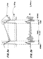
- FIGURES 2a-2c illustrates waveforms useful in explaining the operation of the high voltage power supply of FIGURE 1. Similar numbers and symbols in FIGURE 1 and in 2a-2c indicate similiar items or functions.
- transistor Q1 of FIGURE 1 becomes nonconductive, causing a retrace voltage V2 to develop across primary winding W1 of flyback transformer T1 and a retrace voltage V1 to develop across winding W2.
- the waveform of retrace voltage V2 is similar in shape to that of voltage V1 of FIGURE 2a.
- the peak-to-peak amplitude of voltage V2 is approximately 1150V and that of voltage V1 60V.
- corresponding retrace voltages are developed across each winding segment W 3a -W 3d of tertiary winding W3.
- diode D1 of FIGURE 1 is back biased by the +145V that is applied via resistor R2 to the cathode of diode D1.
- a voltage V3 at terminal 150a has an average value that is equal to +145V during trace and at the beginning time, t1, of retrace of FIGURE 2c.
- resister R2 does not increase the output impedance at ultor terminal 150b during interval t c of FIGURE 2c.
- current i2 of FIGURE 1 charges the ultor capacitance formed by the CRT, not shown.
- the oscillation frequency is determined in accordance with the resonance frequency to which a resonance circuit that includes the leakage inductance of transformer T1 is tuned.
- the result is that the output impedance at ultor terminal 150b is advantageously low, that provides better ultor voltage regulation as a function of beam current than if resistor R2 were not bypassed.
- damping arrangement 120 can be used together with the beam current sampling resistor R1.
- diodes D a , D b , D c , and D d become non-conductive, and ringing current i2 of FIGURE 2b produces a high amplitude of ringing in voltage V3 of FIGURE 2c, developed across damping resistor R2 of FIGURE 1.
- FIGURES 3a and 3b illustrate waveforms of a modified arrangement of FIGURE 1 in which resistor R2 of FIGURE 1 is removed, in which a larger resistor of 10k ⁇ is substituted for resistor R1 of FIGURE 1 having a value of 4.7 k ⁇ and in which diode D1 of FIGURE 1 is replaced by a jumper wire 55, all as shown by dash lines in FIGURE 1.
- Such modified arrangement does not include damping arrangement 120 of the invention.
- Similar numbers and symbols in FIGUREs 2a-2c and in FIGUREs 3a-3b indicate similar items or functions.
- the value of resistor R1, in the unmodified arrangement is smaller. This is so because of the higher DC voltage level developed in resistor R1 as a result of the rectification caused by diode D1 in the unmodified arrangement.
Landscapes
- Engineering & Computer Science (AREA)
- Multimedia (AREA)
- Signal Processing (AREA)
- Details Of Television Scanning (AREA)
- Television Receiver Circuits (AREA)
- Rectifiers (AREA)
- Dc-Dc Converters (AREA)
Applications Claiming Priority (4)
| Application Number | Priority Date | Filing Date | Title |
|---|---|---|---|
| GB888807209A GB8807209D0 (en) | 1988-03-25 | 1988-03-25 | Reduction of flyback transformer ringing |
| GB8807209 | 1988-03-25 | ||
| US238631 | 1988-08-31 | ||
| US07/238,631 US4866353A (en) | 1988-03-25 | 1988-08-31 | Arrangement for reducing ringing in a flyback transformer |
Publications (3)
| Publication Number | Publication Date |
|---|---|
| EP0334658A2 true EP0334658A2 (de) | 1989-09-27 |
| EP0334658A3 EP0334658A3 (en) | 1990-06-27 |
| EP0334658B1 EP0334658B1 (de) | 1994-02-09 |
Family
ID=26293691
Family Applications (1)
| Application Number | Title | Priority Date | Filing Date |
|---|---|---|---|
| EP89302926A Expired - Lifetime EP0334658B1 (de) | 1988-03-25 | 1989-03-23 | Stromversorgungsanordnung |
Country Status (8)
| Country | Link |
|---|---|
| EP (1) | EP0334658B1 (de) |
| JP (1) | JP3120850B2 (de) |
| CN (1) | CN1018042B (de) |
| CA (1) | CA1300744C (de) |
| DE (1) | DE68912956T2 (de) |
| ES (1) | ES2049809T3 (de) |
| FI (1) | FI91702C (de) |
| TR (1) | TR26306A (de) |
Cited By (2)
| Publication number | Priority date | Publication date | Assignee | Title |
|---|---|---|---|---|
| EP0521659A2 (de) * | 1991-07-01 | 1993-01-07 | RCA Thomson Licensing Corporation | Hochspannungsstabilisierkreis für Videoanzeigegerät |
| ES2043486A1 (es) * | 1990-04-30 | 1993-12-16 | Thomson Consumer Electronics | Circuito de estabilizacion de alta tension para un aparato de presentacion de video. |
Families Citing this family (1)
| Publication number | Priority date | Publication date | Assignee | Title |
|---|---|---|---|---|
| JP6437959B2 (ja) * | 2016-06-30 | 2018-12-12 | トヨタ自動車株式会社 | 電力変換装置 |
Citations (4)
| Publication number | Priority date | Publication date | Assignee | Title |
|---|---|---|---|---|
| FR2069983A1 (de) * | 1969-12-19 | 1971-09-10 | Videon Sa | |
| US3745246A (en) * | 1971-04-03 | 1973-07-10 | Victor Company Of Japan | High voltage producing circuit for television receivers |
| JPS5531380A (en) * | 1978-08-28 | 1980-03-05 | Matsushita Electric Ind Co Ltd | Screen voltage removing circuit of television set |
| US4272705A (en) * | 1979-09-14 | 1981-06-09 | Zenith Radio Corporation | Anti-ringing circuit for CRT deflection yoke |
Family Cites Families (3)
| Publication number | Priority date | Publication date | Assignee | Title |
|---|---|---|---|---|
| JPS58429B2 (ja) * | 1974-08-07 | 1983-01-06 | ヒサミツセイヤク カブシキガイシヤ | シンキナ 2− オキソ −1,2,3,4− テトラヒドロピリド ( 2,3−d ) ピリミジンユウドウタイ オヨビ ソノサンフカエンノ セイゾウホウ |
| JPS576346A (en) * | 1980-06-13 | 1982-01-13 | Hitachi Ltd | Nmr lock circuit |
| JPS57102264U (de) * | 1980-12-12 | 1982-06-23 |
-
1989
- 1989-02-02 CA CA000589980A patent/CA1300744C/en not_active Expired - Fee Related
- 1989-03-09 TR TR89/0210A patent/TR26306A/xx unknown
- 1989-03-17 FI FI891282A patent/FI91702C/fi not_active IP Right Cessation
- 1989-03-23 ES ES89302926T patent/ES2049809T3/es not_active Expired - Lifetime
- 1989-03-23 DE DE68912956T patent/DE68912956T2/de not_active Expired - Lifetime
- 1989-03-23 CN CN89101617A patent/CN1018042B/zh not_active Expired
- 1989-03-23 EP EP89302926A patent/EP0334658B1/de not_active Expired - Lifetime
- 1989-03-24 JP JP01073715A patent/JP3120850B2/ja not_active Expired - Fee Related
Patent Citations (4)
| Publication number | Priority date | Publication date | Assignee | Title |
|---|---|---|---|---|
| FR2069983A1 (de) * | 1969-12-19 | 1971-09-10 | Videon Sa | |
| US3745246A (en) * | 1971-04-03 | 1973-07-10 | Victor Company Of Japan | High voltage producing circuit for television receivers |
| JPS5531380A (en) * | 1978-08-28 | 1980-03-05 | Matsushita Electric Ind Co Ltd | Screen voltage removing circuit of television set |
| US4272705A (en) * | 1979-09-14 | 1981-06-09 | Zenith Radio Corporation | Anti-ringing circuit for CRT deflection yoke |
Non-Patent Citations (1)
| Title |
|---|
| PATENT ABSTRACTS OF JAPAN vol. 4, no. 63 (E-10)(545), 13 May 1980; & JP - A - 55 031 380 (MATSUSHITA) 05-03-1980 * |
Cited By (6)
| Publication number | Priority date | Publication date | Assignee | Title |
|---|---|---|---|---|
| ES2043486A1 (es) * | 1990-04-30 | 1993-12-16 | Thomson Consumer Electronics | Circuito de estabilizacion de alta tension para un aparato de presentacion de video. |
| DE4113922B4 (de) * | 1990-04-30 | 2006-04-27 | Thomson Consumer Electronics, Inc., Indianapolis | Schaltungsanordnung zur Stabilisierung der Hochspannung für ein Video-Bildwiedergabegerät |
| EP0521659A2 (de) * | 1991-07-01 | 1993-01-07 | RCA Thomson Licensing Corporation | Hochspannungsstabilisierkreis für Videoanzeigegerät |
| EP0521659A3 (de) * | 1991-07-01 | 1994-04-27 | Rca Thomson Licensing Corp | |
| EP0876054A2 (de) * | 1991-07-01 | 1998-11-04 | RCA Thomson Licensing Corporation | Hochspannungsstabilisierkreis für Videoanzeigegerät |
| EP0876054A3 (de) * | 1991-07-01 | 1999-08-04 | RCA Thomson Licensing Corporation | Hochspannungsstabilisierkreis für Videoanzeigegerät |
Also Published As
| Publication number | Publication date |
|---|---|
| FI891282A (fi) | 1989-09-26 |
| JP3120850B2 (ja) | 2000-12-25 |
| DE68912956D1 (de) | 1994-03-24 |
| FI91702B (fi) | 1994-04-15 |
| FI91702C (fi) | 1994-07-25 |
| JPH01286577A (ja) | 1989-11-17 |
| EP0334658B1 (de) | 1994-02-09 |
| DE68912956T2 (de) | 1994-08-18 |
| FI891282A0 (fi) | 1989-03-17 |
| TR26306A (tr) | 1995-03-15 |
| ES2049809T3 (es) | 1994-05-01 |
| EP0334658A3 (en) | 1990-06-27 |
| CN1018042B (zh) | 1992-08-26 |
| CN1036868A (zh) | 1989-11-01 |
| CA1300744C (en) | 1992-05-12 |
Similar Documents
| Publication | Publication Date | Title |
|---|---|---|
| US4329729A (en) | Side pincushion modulator circuit with overstress protection | |
| GB2140640A (en) | Deflection circuit | |
| EP0588114A2 (de) | Horizontale Ablenkungswellenform-Korrektionsschaltung | |
| US4099101A (en) | Circuit in a television display apparatus for producing a sawtooth deflection current through a line deflection coil | |
| JP3571086B2 (ja) | テレビジョン装置用電源 | |
| GB2141845A (en) | Deflection circuit | |
| EP0334658B1 (de) | Stromversorgungsanordnung | |
| US4866353A (en) | Arrangement for reducing ringing in a flyback transformer | |
| CA1213365A (en) | High dc voltage generator | |
| EP0546595B1 (de) | Dynamische Fokussierungsschaltung für Kathodenstrahlröhre und Transformator hierfür | |
| US4607195A (en) | Picture display device comprising a power supply circuit and a line deflection circuit | |
| EP0183514A2 (de) | Dynamische Fokussierschaltung | |
| US4381477A (en) | Circuit for a picture display device for converting an input d.c. voltage into an output d.c. voltage | |
| US5043638A (en) | Dynamic focus adjusting voltage generating circuit | |
| US4572993A (en) | Television deflection circuit with raster width stabilization | |
| KR900005363B1 (ko) | 음극선관을 위한 수평 출력회로 | |
| US4425533A (en) | Generator for producing a d.c. supply voltage in a television receiver comprising a vertical scanning circuit | |
| CA2000524C (en) | Power supply protection circuit | |
| US4084115A (en) | Circuit for correcting setup error in a color television receiver | |
| US4441058A (en) | Deflection circuit with linearity correction | |
| US4187451A (en) | Color picture display device with a circuit for generating a screen grid voltage | |
| JPS596672A (ja) | 水平偏向電流発生回路配置 | |
| EP0266996B1 (de) | Schaltung zur Rasterkorrektur | |
| EP0114430B1 (de) | Bildwiedergabegerät versehen mit einer Speiseschaltung und einer Zeilenablenkschaltung | |
| GB1574506A (en) | Line sawtooth deflection current generator |
Legal Events
| Date | Code | Title | Description |
|---|---|---|---|
| PUAI | Public reference made under article 153(3) epc to a published international application that has entered the european phase |
Free format text: ORIGINAL CODE: 0009012 |
|
| AK | Designated contracting states |
Kind code of ref document: A2 Designated state(s): DE ES FR GB IT SE |
|
| PUAL | Search report despatched |
Free format text: ORIGINAL CODE: 0009013 |
|
| AK | Designated contracting states |
Kind code of ref document: A3 Designated state(s): DE ES FR GB IT SE |
|
| 17P | Request for examination filed |
Effective date: 19901122 |
|
| RAP1 | Party data changed (applicant data changed or rights of an application transferred) |
Owner name: RCA THOMSON LICENSING CORPORATION |
|
| 17Q | First examination report despatched |
Effective date: 19921001 |
|
| GRAA | (expected) grant |
Free format text: ORIGINAL CODE: 0009210 |
|
| AK | Designated contracting states |
Kind code of ref document: B1 Designated state(s): DE ES FR GB IT SE |
|
| REF | Corresponds to: |
Ref document number: 68912956 Country of ref document: DE Date of ref document: 19940324 |
|
| ET | Fr: translation filed | ||
| ITF | It: translation for a ep patent filed |
Owner name: ING. C. GREGORJ S.P.A. |
|
| REG | Reference to a national code |
Ref country code: ES Ref legal event code: FG2A Ref document number: 2049809 Country of ref document: ES Kind code of ref document: T3 |
|
| PLBE | No opposition filed within time limit |
Free format text: ORIGINAL CODE: 0009261 |
|
| STAA | Information on the status of an ep patent application or granted ep patent |
Free format text: STATUS: NO OPPOSITION FILED WITHIN TIME LIMIT |
|
| EAL | Se: european patent in force in sweden |
Ref document number: 89302926.4 |
|
| 26N | No opposition filed | ||
| REG | Reference to a national code |
Ref country code: GB Ref legal event code: 732E |
|
| REG | Reference to a national code |
Ref country code: GB Ref legal event code: IF02 |
|
| REG | Reference to a national code |
Ref country code: FR Ref legal event code: D6 |
|
| PGFP | Annual fee paid to national office [announced via postgrant information from national office to epo] |
Ref country code: SE Payment date: 20030207 Year of fee payment: 15 |
|
| PGFP | Annual fee paid to national office [announced via postgrant information from national office to epo] |
Ref country code: ES Payment date: 20030313 Year of fee payment: 15 |
|
| REG | Reference to a national code |
Ref country code: GB Ref legal event code: 746 Effective date: 20030228 |
|
| PG25 | Lapsed in a contracting state [announced via postgrant information from national office to epo] |
Ref country code: SE Free format text: LAPSE BECAUSE OF NON-PAYMENT OF DUE FEES Effective date: 20040324 Ref country code: ES Free format text: LAPSE BECAUSE OF NON-PAYMENT OF DUE FEES Effective date: 20040324 |
|
| EUG | Se: european patent has lapsed | ||
| REG | Reference to a national code |
Ref country code: ES Ref legal event code: FD2A Effective date: 20040324 |
|
| PGFP | Annual fee paid to national office [announced via postgrant information from national office to epo] |
Ref country code: GB Payment date: 20060123 Year of fee payment: 18 |
|
| PGFP | Annual fee paid to national office [announced via postgrant information from national office to epo] |
Ref country code: DE Payment date: 20060322 Year of fee payment: 18 |
|
| PGFP | Annual fee paid to national office [announced via postgrant information from national office to epo] |
Ref country code: FR Payment date: 20060330 Year of fee payment: 18 |
|
| PGFP | Annual fee paid to national office [announced via postgrant information from national office to epo] |
Ref country code: IT Payment date: 20060331 Year of fee payment: 18 |
|
| GBPC | Gb: european patent ceased through non-payment of renewal fee |
Effective date: 20070323 |
|
| REG | Reference to a national code |
Ref country code: FR Ref legal event code: ST Effective date: 20071130 |
|
| PG25 | Lapsed in a contracting state [announced via postgrant information from national office to epo] |
Ref country code: DE Free format text: LAPSE BECAUSE OF NON-PAYMENT OF DUE FEES Effective date: 20071002 |
|
| PG25 | Lapsed in a contracting state [announced via postgrant information from national office to epo] |
Ref country code: GB Free format text: LAPSE BECAUSE OF NON-PAYMENT OF DUE FEES Effective date: 20070323 |
|
| PG25 | Lapsed in a contracting state [announced via postgrant information from national office to epo] |
Ref country code: FR Free format text: LAPSE BECAUSE OF NON-PAYMENT OF DUE FEES Effective date: 20070402 |
|
| PG25 | Lapsed in a contracting state [announced via postgrant information from national office to epo] |
Ref country code: IT Free format text: LAPSE BECAUSE OF NON-PAYMENT OF DUE FEES Effective date: 20070323 |