EP0314178B1 - Circuit d'amorçage pour lampes à haute pression et à vapeur métallique - Google Patents
Circuit d'amorçage pour lampes à haute pression et à vapeur métallique Download PDFInfo
- Publication number
- EP0314178B1 EP0314178B1 EP88118033A EP88118033A EP0314178B1 EP 0314178 B1 EP0314178 B1 EP 0314178B1 EP 88118033 A EP88118033 A EP 88118033A EP 88118033 A EP88118033 A EP 88118033A EP 0314178 B1 EP0314178 B1 EP 0314178B1
- Authority
- EP
- European Patent Office
- Prior art keywords
- choke coil
- ignition
- capacitor
- voltage
- lamp
- Prior art date
- Legal status (The legal status is an assumption and is not a legal conclusion. Google has not performed a legal analysis and makes no representation as to the accuracy of the status listed.)
- Expired - Lifetime
Links
Images

Classifications
-
- H—ELECTRICITY
- H05—ELECTRIC TECHNIQUES NOT OTHERWISE PROVIDED FOR
- H05B—ELECTRIC HEATING; ELECTRIC LIGHT SOURCES NOT OTHERWISE PROVIDED FOR; CIRCUIT ARRANGEMENTS FOR ELECTRIC LIGHT SOURCES, IN GENERAL
- H05B41/00—Circuit arrangements or apparatus for igniting or operating discharge lamps
- H05B41/02—Details
- H05B41/04—Starting switches
- H05B41/042—Starting switches using semiconductor devices
Definitions
- the invention relates to an ignition circuit for a high-pressure metal vapor discharge lamp according to the preamble of claim 1.
- Such an ignition circuit is the subject of DE-OS 31 08 547. It is also shown in FIG.
- the series inductance is formed by a choke with only one winding.
- the series inductance and the series circuit comprising the surge capacitor and the auxiliary ignition capacitor represent a filter element. It is assumed that a positive half-wave begins after the ignition circuit is switched on to the AC network. In this case, the voltage across the surge capacitor increases with the positive half-wave. The voltage rise at the surge capacitor depends on the series inductance. The larger this is, the less the voltage increase. When the voltage across the surge capacitor reaches a certain voltage threshold, the switching element switches through, with the result that the surge capacitor discharges through the now conductive switching element and a surge occurs at the connection point between the surge capacitor and the series inductance. This surge can be several kV and leads to ionization of the lamp.
- the series resonance circuit consisting of the series inductance and the auxiliary ignition capacitor is excited to an oscillation, which is however decaying because it is damped by the ionized tube, among other things. If the tube does not ignite, the ionization will decrease again.
- the resonance frequency of the series resonance circuit mentioned is so chosen so that at least the half-wave of the decaying vibration following the surge voltage still occurs at a time when the tube is still ionized. When the vibration subsides below the voltage threshold mentioned, the switch element becomes non-conductive again. If the lamp has not yet ignited, the process described is repeated.
- the lamp manufacturers stipulate that at least three ignition pulses should be generated for a safe ignition per half-wave, the time interval between which is not more than 0.3 ms.
- the series inductance formed by the choke winding limits the lamp current. From the above description it follows that the dimensioning of the ballast inductance is the function of the ignition circuit of essential importance. This is because the series inductance determines the distance between the ignition pulses, the frequency of the decaying oscillation and the current flowing through the lamp after ignition.
- the invention has for its object to modify an ignition circuit of the type described in the preamble of claim 1 in such a way that it can also be used for high-pressure metal vapor discharge lamps of lower power than previously, the prescribed time interval between the ignition pulses and the resonance frequency of the ballast inductance and the auxiliary ignition capacitor formed series resonance circuit should remain essentially unchanged.
- the first-mentioned choke winding determines the time interval between the ignition pulses and the frequency of the decaying oscillation, while the entirety of both choke windings determines the current flowing through the lamp.
- the ignition circuit according to the invention is particularly simple and inexpensive to manufacture if both choke windings have a common choke core.
- claims 5 to 7 relate to measures which prevent a high-frequency voltage dropping at the further choke winding from exceeding a certain voltage value. As described at the beginning, the high-frequency voltage should drop across the lamp in order to contribute to its ignition.
- the ignition circuit shown in FIG. 1 is provided with two connections 1, 2 for the AC network and is used to ignite a high-pressure metal vapor discharge lamp 5.
- One electrode of lamp 5 is connected to network connection 2.
- the other electrode of lamp 5 is equipped with a superimposed ignition voltage device 4 connected.
- a series inductance 3, which is formed by a choke with a single winding, is connected upstream of the superimposed ignition voltage device 4.
- the ballast inductor 3 is on the one hand at the AC mains connection 1 and on the other hand is connected to a connection of the surge capacitor 6.
- the other terminal of a surge capacitor 6 is connected to a terminal of an auxiliary ignition capacitor 7.
- the other connection of the auxiliary ignition capacitor 7 is connected to the AC mains connection 2.
- a resistor 8 is connected in parallel to the auxiliary ignition capacitor 7, which ensures compliance with the desired operating voltage range and the given limits for the phase position of the ignition pulses.
- the connection point between the surge capacitor 6 and the auxiliary ignition capacitor 7 is connected to a connection of a switch element 9 via a high-frequency coil 14. In the present case, this is a Sidac.
- This switch element is normally non-conductive. It becomes conductive when the voltage applied to it exceeds a certain threshold voltage value. This applies in both polarity directions.
- the switch element 9 can also be a four-layer diode, for example.
- the other connection of the switch element 9 is connected to a connection 15 of a pulse transformer 10 connected as an autotransformer.
- the other terminal 16 of the pulse transformer 10 is connected to the lamp 5.
- the pulse transformer 10 is provided with a tap 13 which is connected to the connection point between the ballast inductor 3 and the surge capacitor 6.
- the primary winding lies between one connection 15 and the tap 13.
- the secondary winding lies between the tap 13 and the other connection 16.
- a transformer with separate primary and secondary windings can also be used.
- the ignition circuit described above can be used for high-pressure metal vapor discharge lamps which have a power of approximately 150W.
- the known circuit works as follows: If the AC network is connected to the connections 1 and 2 and, for example, a positive half-wave begins, the surge capacitor 6 and the auxiliary ignition capacitor 7 are charged via the series inductance 3 during the rising phase of the half-wave. If the voltage across the surge capacitor 6 exceeds the voltage threshold value specified by the switch element 9, the switch element 9 switches through, ie there is a sudden change from the non-conductive state to the conductive state. As a result, the surge capacitor 6 discharges through the switch element 9. This has the consequence that a voltage surge occurs at the tap 13 of the pulse capacitor 12, which imposes a superimposition on the mains voltage at the circuit point 16 and can be several kV. This voltage surge leads to ionization of the lamp 5.
- the series resonance circuit formed from the series inductance 3 and the auxiliary ignition capacitor 7 is triggered, with the result that a damped oscillation is produced.
- This is applied to the primary winding 11 of the pulse transformer 10 and is stepped up, so that after the voltage surge on the lamp 5 there is a decaying high-frequency oscillation of high voltage.
- the resonance frequency of the series resonance circuit formed from the series inductance 3 and the auxiliary capacitor 7 is selected such that at least the first half-wave of the decaying oscillation following the voltage surge strikes the still ionized lamp 5 if the lamp 5 has not already ignited the voltage surge.
- the high-frequency oscillation subsides below the voltage threshold value of the switch element 9 this again non-conductive.
- this process is repeated, at least three times per network half-wave. This is prescribed by the lamp manufacturers for reliable ignition of the lamp 5, the time interval between the ignition pulses not being greater than 0.3 ms.
- the series inductance 3 limits the lamp current to the current corresponding to the nominal power of approximately 150W.
- the series inductance 3 accordingly determines the time interval between the ignition pulses and the frequency of the decaying oscillation and also serves to limit the current flowing through the lamp 5 after ignition.
- the circuits shown in FIGS. 2 to 4 serve to ignite lamps 105, 205 which have a lower output than lamp 5 in FIG. 1. Lamps with a power of 35 or 70W are typical. Such lamps must be limited to a correspondingly lower current because of their lower power consumption.
- the ignition circuit according to FIG. 2 has a series inductance 103 which, as before, is formed by a single choke, which, however, has a further choke winding 108 in addition to a first choke winding 104. Both choke windings 104, 108 sit on the same core.
- the first choke winding 104 is connected like the single choke winding forming the series inductance 3 shown in the known ignition circuit according to FIG. 1.
- the second choke winding 108 is connected between the lamp 105 and the connection 2 of the AC source. It is also bridged by a short-circuit capacitor 106. In this way, only the first choke winding 104 forms a series circuit with the surge capacitor 6 and the auxiliary ignition capacitor 7, with the result that the time interval between the ignition pulses and the resonance frequency of the first choke winding 104 and the auxiliary ignition capacitor 7 formed series resonance circuit remain largely unchanged from the corresponding values of the circuit of Figure 1. On the other hand, if the lamp 105 has ignited, the second choke winding 108 is in the circuit of the lamp in addition to the first choke winding 104, with the result that the lamp current is limited to a correspondingly reduced value.
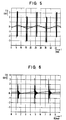
- FIG. 5 shows the time course of the ignition voltage generated at point 16 of the ignition circuit according to FIG. 2. It can be seen that three ignition pulses occur per network half-wave.
- FIG. 6 was created while stretching the time of FIG. 5 and shows three ignition pulses in succession during a network half-wave, it being recognized that the first voltage surge is followed by a decaying oscillation.
- the two choke windings 204, 208 are galvanically connected to one another by the tap 209.
- the first winding 204 is connected on the one hand to the mains connection 1 and on the other hand via the tap 209 to the surge capacitor 6.
- the second winding 208 is on the one hand via the tap 209 to the surge capacitor 6 and on the other hand to the tap 13 of the pulse transformer 10 connected.
- connection of the second winding 208 connected to the tap 13 of the pulse transformer 10 is also connected via a return capacitor 206 connected to the other network connection 2.
- this ignition circuit with the auxiliary ignition capacitor 7 and the surge capacitor 6, in turn only the first winding 204 of the series inductor 203 is in series, as a result of which, as described in connection with the ignition circuit according to FIG. 2, the time interval between the ignition pulses and the resonance frequency compared to the known one Ignition circuit according to Figure 1 remain largely unchanged.
- both windings 204, 208 are in series in the circuit of the lamp, with the result that the lamp current is limited to a correspondingly reduced value.
- the ignition circuit according to FIG. 4 differs from the ignition circuit according to FIG. 3 only in that the second winding 208 of the series inductance 203 is bridged here directly by a return capacitor 210.
- VDR voltage-dependent resistor
Claims (7)
- Circuit d'amorçage pour une lampe à décharge à vapeur métallique à haute pression destinée à être connectée à une source de courant alternatif, de préférence au réseau de distribution de courant alternatif, comprenant une inductance ballast qui est constituée par une bobine d'induction, un condensateur de décharge impulsionnelle, un condensateur de résonance, un élément de commutation qui, dans une direction de polarisation au moins, est conducteur au-delà d'une tension de seuil déterminée et non-conducteur en deçà de cette tension de seuil et un transformateur d'impulsion, la bobine d'induction, le condensateur de décharge impulsionnelle et le condensateur d'amorçage formant un premier circuit série connecté à la source de courant alternatif, le condensateur de décharge impulsionnelle étant branché en parallèle avec l'élément de commutation et l'enroulement primaire du transformateur d'impulsion branchés en série et la bobine d'induction, l'enroulement secondaire du transformateur d'impulsion et la lampe formant un deuxième circuit série connecté à la source de courant alternatif, caractérisé par une bobine d'induction (108, 208) supplémentaire qui est branchée dans le deuxième circuit série (104, 12, 105, 108 ou 204, 208, 12, 205).
- Circuit d'amorçage selon la revendication 1, caractérisé par le fait que la bobine d'induction (108, 208) supplémentaire a un noyau de bobine commun avec la première bobine d'induction (104, 204) mentionnée.
- Circuit d'amorçage selon la revendication 1 ou 2, caractérisé par le fait que les deux bobines d'induction (104, 108) sont isolées électriquement et par le fait que la bobine d'induction (108) supplémentaire est branchée entre la lampe (105) et la borne de connexion (2) correspondante de la source de courant alternatif.
- Circuit d'amorçage selon la revendication 1 ou 2, caractérisé par le fait que les deux bobines d'induction (204, 208) sont reliées électriquement entre elles à une extrémité ou font partie d'un transformateur économiseur (10) pourvu d'une prise (13) et par le fait que la bobine d'induction (208) supplémentaire est branchée entre la première bobine d'induction (204) mentionnée et l'enroulement secondaire (12) du transformateur d'impulsions (10).
- Circuit d'amorçage selon la revendication 3 ou 4, caractérisé par le fait que la bobine d'induction (108, 208) supplémentaire est pontée par un élément impédant (106, 210) de pontage qui constitue une résistance de faible valeur pour la haute fréquence engendrée par les impulsions produites ou empêche qu'une différence de potentiel qui chute dans la bobine d'induction (108, 208) supplémentaire soit supérieure à un seuil de tension déterminé.
- Circuit d'amorçage selon la revendication 4, caractérisé par le fait qu'un élément impédant (206) de pontage est placé entre le point de connexion (13) formé par la bobine d'induction (208) supplémentaire et l'enroulement secondaire (12) du transformateur d'impulsions (10) et la borne de connexion (2) du réseau de courant alternatif connectée à la lampe (205), lequel élément impédant constitue une résistance de faible valeur pour la haute fréquence engendrée par les impulsions d'amorçage produites ou empêche qu'une différence de potentiel qui chute dans la bobine d'induction (208) supplémentaire soit supérieure à un seuil de tension déterminé.
- Circuit d'amorçage selon la revendication 5 ou 6, caractérisé par le fait que l'élément impédant de pontage est constitué par un condensateur (106, 206, 210), une combinaison condensateur-résistance ou une résistance dont la valeur est indépendante de la tension.
Applications Claiming Priority (2)
| Application Number | Priority Date | Filing Date | Title |
|---|---|---|---|
| DE3736542 | 1987-10-28 | ||
| DE19873736542 DE3736542A1 (de) | 1987-10-28 | 1987-10-28 | Zuendschaltung fuer eine hochdruckmetalldampfentladungslampe |
Publications (2)
| Publication Number | Publication Date |
|---|---|
| EP0314178A1 EP0314178A1 (fr) | 1989-05-03 |
| EP0314178B1 true EP0314178B1 (fr) | 1994-10-19 |
Family
ID=6339283
Family Applications (1)
| Application Number | Title | Priority Date | Filing Date |
|---|---|---|---|
| EP88118033A Expired - Lifetime EP0314178B1 (fr) | 1987-10-28 | 1988-10-28 | Circuit d'amorçage pour lampes à haute pression et à vapeur métallique |
Country Status (3)
| Country | Link |
|---|---|
| EP (1) | EP0314178B1 (fr) |
| AT (1) | ATE113157T1 (fr) |
| DE (2) | DE3736542A1 (fr) |
Families Citing this family (4)
| Publication number | Priority date | Publication date | Assignee | Title |
|---|---|---|---|---|
| DE4236403A1 (de) * | 1992-10-28 | 1994-07-07 | Tridonic Bauelemente Ges Mbh D | Zündschaltung für eine Hochdruckmetalldampfentladungslampe |
| DE19531622B4 (de) * | 1995-08-28 | 2011-01-13 | Tridonicatco Gmbh & Co. Kg | Zündschaltung für eine Hochdruck-Gasentladungslampe |
| DE19531623B4 (de) * | 1995-08-28 | 2010-09-23 | Tridonicatco Gmbh & Co. Kg | Verfahren und Schaltungsanordnung zum Zünden einer Hochdruck-Gasentladungslampe |
| DE19544842A1 (de) * | 1995-12-01 | 1997-06-05 | Bosch Gmbh Robert | Eingangsbeschaltung für eine Zündvorrichtung einer Hochdruck-Gasentladungslampe |
Family Cites Families (3)
| Publication number | Priority date | Publication date | Assignee | Title |
|---|---|---|---|---|
| GB824906A (en) * | 1957-10-15 | 1959-12-09 | Engelhard Ind Inc | Improvements in or relating to an operating circuit for electrical discharge lamps |
| US4187449A (en) * | 1978-05-08 | 1980-02-05 | General Electric Company | Discharge lamp operating circuit |
| US4538094A (en) * | 1983-08-12 | 1985-08-27 | Iota Engineering Co. | Lamp ballast with near unity power factor and low harmonic content |
-
1987
- 1987-10-28 DE DE19873736542 patent/DE3736542A1/de not_active Withdrawn
-
1988
- 1988-10-28 EP EP88118033A patent/EP0314178B1/fr not_active Expired - Lifetime
- 1988-10-28 AT AT88118033T patent/ATE113157T1/de not_active IP Right Cessation
- 1988-10-28 DE DE3851868T patent/DE3851868D1/de not_active Expired - Fee Related
Also Published As
| Publication number | Publication date |
|---|---|
| DE3851868D1 (de) | 1994-11-24 |
| ATE113157T1 (de) | 1994-11-15 |
| EP0314178A1 (fr) | 1989-05-03 |
| DE3736542A1 (de) | 1989-05-11 |
Similar Documents
| Publication | Publication Date | Title |
|---|---|---|
| EP1211794B1 (fr) | Procédé de regulation de courant de sortie et/ou tension de sortie d'alimentation à découpage | |
| DE3108547A1 (de) | "zuendschaltung fuer eine hochdruckmetalldampfentladungslampe" | |
| DE3108548C2 (de) | Zündschaltung für eine Hochdruckmetalldampfentladungslampe | |
| DE3333768A1 (de) | Vorrichtung zur begrenzung von wechselstroemen | |
| EP0116275A2 (fr) | Compensateur de puissance réactive | |
| EP0868115B1 (fr) | Circuit d'amorçage pour lampe HID | |
| DE69816950T2 (de) | Schaltungsanordnung | |
| DE2758227C3 (de) | dv/dt-Schutzschaltungsanordnung für einen GTO-Thyristor | |
| EP1058488B1 (fr) | Circuit d'allumage pour lampe | |
| EP0914754A1 (fr) | Dispositif d'allumage pour une lampe a decharge et procede pour allumer une lampe a decharge | |
| EP0314178B1 (fr) | Circuit d'amorçage pour lampes à haute pression et à vapeur métallique | |
| DE3204449C2 (fr) | ||
| EP0381083A1 (fr) | Circuit d'amorçage pour une lampe à décharge haute pression à vapeur métallique branchée sur une source alternative via une inductance | |
| EP0178735B1 (fr) | Dispositif de circuit pour enflammer et mettre en marche des lampes à décharge au gaz | |
| EP0212740A2 (fr) | Disposition de circuit pour le démarrage et le fonctionnement de lampes à décharge gazeuse | |
| EP0155729B1 (fr) | Circuit pour l'exploitation à courant alternatif pour lampes à décharge à haute pression | |
| EP0595333B1 (fr) | Circuit d'amorage pour une lampe à décharge hautepression à vapeur métallique | |
| DE2604914C3 (de) | Schaltungsanordnung zum Zünden und zum Betrieb einer Entladungslampe | |
| DE60117764T2 (de) | Zündvorrichtung mit störkapazitätsunterdrücker | |
| DE69514182T2 (de) | Schaltungsanordnung | |
| EP0599887B1 (fr) | Dispositif pour le fonctionnement d'une lampe a decharge | |
| EP2140735B1 (fr) | Ensemble circuit servant à amorcer et à faire fonctionner au moins une lampe à décharge | |
| EP0213354A1 (fr) | Montage de protection contre les claquages dans un circuit émetteur | |
| DE3339814A1 (de) | Zuendschaltung fuer eine hochdruckmetalldampfentladungslampe | |
| DE102004055976A1 (de) | Schaltungsanordnung zum Betrieb einer Hochdruckentladungslampe |
Legal Events
| Date | Code | Title | Description |
|---|---|---|---|
| PUAI | Public reference made under article 153(3) epc to a published international application that has entered the european phase |
Free format text: ORIGINAL CODE: 0009012 |
|
| AK | Designated contracting states |
Kind code of ref document: A1 Designated state(s): AT CH DE FR GB IT LI |
|
| 17P | Request for examination filed |
Effective date: 19891031 |
|
| 17Q | First examination report despatched |
Effective date: 19921214 |
|
| GRAA | (expected) grant |
Free format text: ORIGINAL CODE: 0009210 |
|
| AK | Designated contracting states |
Kind code of ref document: B1 Designated state(s): AT CH DE FR GB IT LI |
|
| REF | Corresponds to: |
Ref document number: 113157 Country of ref document: AT Date of ref document: 19941115 Kind code of ref document: T |
|
| REF | Corresponds to: |
Ref document number: 3851868 Country of ref document: DE Date of ref document: 19941124 |
|
| ET | Fr: translation filed | ||
| ITF | It: translation for a ep patent filed |
Owner name: JACOBACCI CASETTA & PERANI S.P.A. |
|
| GBT | Gb: translation of ep patent filed (gb section 77(6)(a)/1977) |
Effective date: 19950124 |
|
| PLBE | No opposition filed within time limit |
Free format text: ORIGINAL CODE: 0009261 |
|
| STAA | Information on the status of an ep patent application or granted ep patent |
Free format text: STATUS: NO OPPOSITION FILED WITHIN TIME LIMIT |
|
| 26N | No opposition filed | ||
| PGFP | Annual fee paid to national office [announced via postgrant information from national office to epo] |
Ref country code: GB Payment date: 20000925 Year of fee payment: 13 |
|
| PGFP | Annual fee paid to national office [announced via postgrant information from national office to epo] |
Ref country code: FR Payment date: 20001017 Year of fee payment: 13 |
|
| PGFP | Annual fee paid to national office [announced via postgrant information from national office to epo] |
Ref country code: CH Payment date: 20001023 Year of fee payment: 13 Ref country code: AT Payment date: 20001023 Year of fee payment: 13 |
|
| PGFP | Annual fee paid to national office [announced via postgrant information from national office to epo] |
Ref country code: DE Payment date: 20001221 Year of fee payment: 13 |
|
| PG25 | Lapsed in a contracting state [announced via postgrant information from national office to epo] |
Ref country code: GB Free format text: LAPSE BECAUSE OF NON-PAYMENT OF DUE FEES Effective date: 20011028 Ref country code: AT Free format text: LAPSE BECAUSE OF NON-PAYMENT OF DUE FEES Effective date: 20011028 |
|
| PG25 | Lapsed in a contracting state [announced via postgrant information from national office to epo] |
Ref country code: LI Free format text: LAPSE BECAUSE OF NON-PAYMENT OF DUE FEES Effective date: 20011031 Ref country code: CH Free format text: LAPSE BECAUSE OF NON-PAYMENT OF DUE FEES Effective date: 20011031 |
|
| REG | Reference to a national code |
Ref country code: GB Ref legal event code: IF02 |
|
| REG | Reference to a national code |
Ref country code: CH Ref legal event code: PL |
|
| GBPC | Gb: european patent ceased through non-payment of renewal fee |
Effective date: 20011028 |
|
| PG25 | Lapsed in a contracting state [announced via postgrant information from national office to epo] |
Ref country code: FR Free format text: LAPSE BECAUSE OF NON-PAYMENT OF DUE FEES Effective date: 20020628 |
|
| PG25 | Lapsed in a contracting state [announced via postgrant information from national office to epo] |
Ref country code: DE Free format text: LAPSE BECAUSE OF NON-PAYMENT OF DUE FEES Effective date: 20020702 |
|
| REG | Reference to a national code |
Ref country code: FR Ref legal event code: ST |
|
| PG25 | Lapsed in a contracting state [announced via postgrant information from national office to epo] |
Ref country code: IT Free format text: LAPSE BECAUSE OF NON-PAYMENT OF DUE FEES;WARNING: LAPSES OF ITALIAN PATENTS WITH EFFECTIVE DATE BEFORE 2007 MAY HAVE OCCURRED AT ANY TIME BEFORE 2007. THE CORRECT EFFECTIVE DATE MAY BE DIFFERENT FROM THE ONE RECORDED. Effective date: 20051028 |