EP0312116A2 - Automatic electronic parts mounting apparatus - Google Patents
Automatic electronic parts mounting apparatus Download PDFInfo
- Publication number
- EP0312116A2 EP0312116A2 EP88117236A EP88117236A EP0312116A2 EP 0312116 A2 EP0312116 A2 EP 0312116A2 EP 88117236 A EP88117236 A EP 88117236A EP 88117236 A EP88117236 A EP 88117236A EP 0312116 A2 EP0312116 A2 EP 0312116A2
- Authority
- EP
- European Patent Office
- Prior art keywords
- mounting
- sequence
- parts
- patterns
- pattern
- Prior art date
- Legal status (The legal status is an assumption and is not a legal conclusion. Google has not performed a legal analysis and makes no representation as to the accuracy of the status listed.)
- Granted
Links
Images


Classifications
-
- H—ELECTRICITY
- H05—ELECTRIC TECHNIQUES NOT OTHERWISE PROVIDED FOR
- H05K—PRINTED CIRCUITS; CASINGS OR CONSTRUCTIONAL DETAILS OF ELECTRIC APPARATUS; MANUFACTURE OF ASSEMBLAGES OF ELECTRICAL COMPONENTS
- H05K13/00—Apparatus or processes specially adapted for manufacturing or adjusting assemblages of electric components
- H05K13/04—Mounting of components, e.g. of leadless components
- H05K13/0404—Pick-and-place heads or apparatus, e.g. with jaws
- H05K13/0413—Pick-and-place heads or apparatus, e.g. with jaws with orientation of the component while holding it; Drive mechanisms for gripping tools, e.g. lifting, lowering or turning of gripping tools
-
- H—ELECTRICITY
- H05—ELECTRIC TECHNIQUES NOT OTHERWISE PROVIDED FOR
- H05K—PRINTED CIRCUITS; CASINGS OR CONSTRUCTIONAL DETAILS OF ELECTRIC APPARATUS; MANUFACTURE OF ASSEMBLAGES OF ELECTRICAL COMPONENTS
- H05K13/00—Apparatus or processes specially adapted for manufacturing or adjusting assemblages of electric components
- H05K13/08—Monitoring manufacture of assemblages
- H05K13/085—Production planning, e.g. of allocation of products to machines, of mounting sequences at machine or facility level
-
- Y—GENERAL TAGGING OF NEW TECHNOLOGICAL DEVELOPMENTS; GENERAL TAGGING OF CROSS-SECTIONAL TECHNOLOGIES SPANNING OVER SEVERAL SECTIONS OF THE IPC; TECHNICAL SUBJECTS COVERED BY FORMER USPC CROSS-REFERENCE ART COLLECTIONS [XRACs] AND DIGESTS
- Y10—TECHNICAL SUBJECTS COVERED BY FORMER USPC
- Y10T—TECHNICAL SUBJECTS COVERED BY FORMER US CLASSIFICATION
- Y10T29/00—Metal working
- Y10T29/53—Means to assemble or disassemble
- Y10T29/5313—Means to assemble electrical device
- Y10T29/53174—Means to fasten electrical component to wiring board, base, or substrate
- Y10T29/53178—Chip component
-
- Y—GENERAL TAGGING OF NEW TECHNOLOGICAL DEVELOPMENTS; GENERAL TAGGING OF CROSS-SECTIONAL TECHNOLOGIES SPANNING OVER SEVERAL SECTIONS OF THE IPC; TECHNICAL SUBJECTS COVERED BY FORMER USPC CROSS-REFERENCE ART COLLECTIONS [XRACs] AND DIGESTS
- Y10—TECHNICAL SUBJECTS COVERED BY FORMER USPC
- Y10T—TECHNICAL SUBJECTS COVERED BY FORMER US CLASSIFICATION
- Y10T29/00—Metal working
- Y10T29/53—Means to assemble or disassemble
- Y10T29/5313—Means to assemble electrical device
- Y10T29/53191—Means to apply vacuum directly to position or hold work part
-
- Y—GENERAL TAGGING OF NEW TECHNOLOGICAL DEVELOPMENTS; GENERAL TAGGING OF CROSS-SECTIONAL TECHNOLOGIES SPANNING OVER SEVERAL SECTIONS OF THE IPC; TECHNICAL SUBJECTS COVERED BY FORMER USPC CROSS-REFERENCE ART COLLECTIONS [XRACs] AND DIGESTS
- Y10—TECHNICAL SUBJECTS COVERED BY FORMER USPC
- Y10T—TECHNICAL SUBJECTS COVERED BY FORMER US CLASSIFICATION
- Y10T29/00—Metal working
- Y10T29/53—Means to assemble or disassemble
- Y10T29/5313—Means to assemble electrical device
- Y10T29/53261—Means to align and advance work part
Definitions
- the chip part is conveyed above the X-Y table 10 upon intermittent rotation of the turntable T, and is mounted on the printed board 11 placed on the X-Y table 10.
- the mounting position of the chip part 1 to be mounted on the board 11 is adjusted by the horizontal movement of the X-Y table 10.
- the angle setting of the chip part 1 is performed by rotating the suction nozzle 6 itself chucking the chip part 1, which is not shown in the drawings.
- chip parts 1 are mounted on the printed board 11 in a plurality of identical patterns and independent patterns having no correlation therewith as shown in a fifth embodiment in Fig. 13, NC data shown in Fig. 14 is used.
- the chip parts 1 are mounted for eight identical patterns in accordance with a forward sequence, and then the chip parts are mounted for two independent patterns which are different from each other.
Abstract
Description
- The present invention relates to an automatic electronic parts mounting apparatus and, more particularly, to an automatic electronic parts mounting apparatus in which when various chip type electronic parts (to be referred to as chip parts hereinafter), e.g., resistors, capacitors, and transistors are automatically positioned/mounted on a printed board placed on an X-Y table in a plurality of different types of patterns constituted by identical patterns and independent patterns having no correlation therewith chip parts having different shapes and sizes can be selectively positioned/mounted by sorting them in accordance with their forms.
- In a conventional automatic electronic parts mounting apparatus of this type, as disclosed in, e.g., U.S. Patent 4,653,664, chip parts having different shapes and sizes are selectively fed from a parts feed means in which they are stored in parts storage tapes wound around the respective tape reels in accordance with their forms and types, the fed chip parts are chucked by a plurality of suction nozzles, which are formed on the periphery of a rotary type index table, at predetermined suction positions, the index table is intermittently rotated so as to convey the chip parts to corresponding parts mounting positions on a printed board placed on an X-Y table, and the chip parts are automatically positioned/mounted at predetermined mounting positions on the printed board by moving the X-Y table in the X-Y directions. Apparatuses having such an arrangement have been developed and put into practical use.
- An operation of such a conventional mounting apparatus is generally controlled by programs. In addition, in the above apparatus, when chip parts are mounted on a single printed board in a plurality of identical patterns by repeating the same pattern, and the same mounting operation is repeated in accordance with the same pattern formation direction.
- For this reason, in the identical mounting patterns formed on the single printed board, the final parts mounting position of a given pattern and the initial mounting position of the next pattern may be greatly separated, and hence a considerably long period of time is required to move the X-Y table. In addition, since all the patterns formed on the printed board are oriented in the same direction, forming the patterns on the printed board is uniformly limited, and efficient patterning becomes impossible. Therefore, a large portion of a board material is wasted.
- Recently, as various types of mounting patterns are produced in small quantities, various patterns tend to be formed in a single printed board. When a plurality of identical patterns and independent patterns having no correlation therewith are formed in a printed board by mounting various chip parts having different shapes and sizes together in this manner, since the above-described process in which the same pattern is repeatedly formed cannot be used, the identical patterns and the independent patterns are sorted, and positioning/mounting must be independently performed in units of sorted patterns, thereby extremely complicating the process.
- In addition, when chip parts having different shapes and sizes are to be mounted on a single printed board together, if a large chip part or a chip part with a high center of gravity is mounted first, a positional error due to an inertial force tends occur because the frequency of movement of such a chip part upon high-speed movement of the X-Y table is higher than that of a small chip part or a chip part with a low center of gravity to be mounted next.
- The present invention has been made to eliminate the drawbacks of the above-described conventional automatic electronic parts mounting apparatus. It is an object of present invention to efficiently perform parts mounting by changing the parts mounting sequence for each mounting pattern in accordance with the formation state of a mounting pattern. In order to achieve this object, according to the present invention, there is provided an automatic electronic parts mounting apparatus for mounting chip parts having different shapes and sizes repeatedly in a plurality of identical mounting patterns on a single printed board placed on an X-Y table which is moved at high speed in the X-Y directions, comprising a pattern storage means for storing NC (Numerical Control) data of the mounting patterns, a pattern position storage section for storing data representing positions on the board where the mounting patterns based on the NC data stored in the pattern storage means are formed, a sequence designating means, arranged in correspondence with the pattern position storage means, for designating a mounting sequence of the chip parts for the mounting patterns, a positioning unit for adjusting a positional relationship between a predetermined position and the chip part by moving the X-Y table at high speed when the chip part designated by the sequence designating means is mounted at the predetermined position on the board, and control means for controlling the positioning unit so as to mount the chip parts corresponding to the mounting patterns stored in the pattern storage section at predetermined positions stored in the pattern storage means in the sequence designated by the sequence designating means.
- It is another object of the present invention to efficiently form a pattern on a board and eliminate waste of a board material by causing the pattern position storage means to store data representing a direction in which a mounting pattern based on the NC data is formed on the board.
- It is still another object of the present invention to perform positioning/mounting without sorting the identical and independent patterns so as to increase the process speed by a simple, collective parts mounting process. In sequence to achieve this object, according to the present invention, there is provided an automatic electronic parts mounting apparatus for mounting chip parts having different shapes and sizes repeatedly in a plurality of patterns including identical mounting patterns and independent patterns having ano correlation therewith on a single printed board placed on an X-Y table which is moved at high speed in the X-Y directions, comprising a pattern storage means for storing NC data of both the identical and independent mounting patterns, a pattern position storage means for storing data representing positions and directions on the board in accordance with which both the identical and independent mounting patterns based on the NC data stored in the pattern storage means are formed, a sequence designating means, arranged in correspondence with the pattern position storage means, for designating a mounting sequence of the chip parts for both the identical and independent mounting patterns, a positioning unit for adjusting a positional relationship between a predetermined position and the chip part by moving the X-Y table at high speed when the chip part designated by the sequence designating means is mounted at the predetermined position on the board, and control means for controlling the positioning unit so as to mount the chip parts corresponding to both the identical and independent mounting patterns stored in the pattern storage means at predetermined positions stored in the pattern storage means in the sequence designated by the sequence designating means.
- It is still another object of the present invention to prevent a positional error of a chip part due to an inertial force upon high-speed movement of the X-Y table and increase precision in mounting the chip parts by sorting/designating the chip parts as groups by the sequence designating means in a mounting sequence in which a positional error due to high-speed movement of the X-Y table is relatively smaller.
-
- Fig. 1 is a schematic perspective view showing an overall arrangement of an automatic electronic parts mounting apparatus according to an embodiment of the present invention;
- Fig. 2 is a block diagram showing a control section of the apparatus in Fig. 1;
- Fig. 3 is a view illustrating a set state of NC data in the apparatus in Fig. 1;
- Fig. 4 is a flow chart showing a sequence of control for mounting chip parts in the apparatus in Fig; 1.
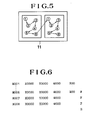
- Fig. 5 is a view illustrating a mounting state of chip parts on a printed board and a mounting sequence in the apparatus in Fig. 1 according to a first embodiment;
- Fig. 6 is a view illustrating an example of setting NC data in the apparatus in Fig. 1 according to the first embodiment;
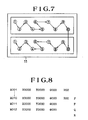
- Fig. 7 is a view illustrating a mounting state of chip parts on a printed board and a mounting sequence in the apparatus in Fig. 1 according to a second embodiment;
- Fig. 8 is a view illustrating an example of setting NC data in the apparatus in Fig. 1 according to the second embodiment;
- Fig. 9 is a view illustrating a mounting state of chip parts on a printed board and a mounting sequence in the apparatus in Fig. 1 according to a third embodiment;
- Fig. 10 is a view illustrating an example of setting NC data in the apparatus in FIg. 1 according to the third embodiment;
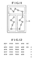
- Fig. 11 is a view illustrating a mounting state of chip parts on a printed board and a mounting sequence in the apparatus in Fig. 1 according to a fourth embodiment;
- Fig. 12 is a view illustrating an example of setting NC data in the apparatus in Fig. 1 according to the fourth embodiment;
- Fig. 13 is a view illustrating a mounting state of chip parts on a printed board and a mounting sequence in the apparatus in Fig. 1 according to a fifth embodiment;
- Fig. 14 is a view illustrating an example of setting NC data in the apparatus in Fig. 1 according to the fifth embodiment;
- Fig. 15 is a schematic plan view showing a mounting state of electronic parts on a printed board according to another embodiment of the present invention; and
- Fig. 16 is a view illustrating an example of setting NC data in the apparatus in Fig. 1 according to a sixth embodiment.
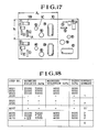
- Fig. 17 is a schematic plan view showing a mounting state of electronic parts on a printed board according to furthermore another embodiment of the present invention.
- Fig. 18 is a view illustrating a set state of NC data when chip parts are mounted on a printed board in a mounting sequence as shown in Fig. 17.
- A parts feeding unit according to embodiments of the present invention will be described in detail below with reference to the accompanying drawings.
- Fig. 1 is a perspective view showing an overall arrangement of an automatic electronic parts mounting apparatus according to the present invention.
Reference numerals 1 denote chip parts which are stored in electronicparts storage tapes 2 at regular spaces. The electronicparts storage tapes 2 are wound aroundcorresponding tape reels 3. The electronicparts storage tapes 2 are fed by a pitch from thetape reels 3 through conveyunits 4. Thetape reels 3 and theconvey units 4 are arranged on a tape moving table 5 which moves reciprocatively in the direction of X so as to constitute a parts feed means. - Referring to Fig. 1 reference symbol T denotes a turntable which is intermittently rotatable.
Reference numerals 6 denotes suction nozzles arranged on the turntable T. Eachsuction nozzle 6 chucks one of thechip parts 1 from a corresponding electronicparts storage tape 2 selected in accordance with the moving state of the tape moving table 5 and conveys it onto a printed board placed on an X-Y table (to be described later) upon rotation of the turntable T. - In addition,
reference numeral 7 denotes a positioning unit for correcting a positional error of thechip part 1 chucked by each suction nozzle in the X-Y directions and also for setting a mounting angle of the chip part; and 8 and 9, pulse motors for horizontally moving an X-Y table 10, on which a printedboard 11 is placed, in the X-Y directions. - More specifically, after the chucked state of the
chip part 1 chucked by thesuction nozzle 6 is corrected by thepositioning unit 7 and also the mounting angle is set, the chip part is conveyed above the X-Y table 10 upon intermittent rotation of the turntable T, and is mounted on the printedboard 11 placed on the X-Y table 10. In addition, the mounting position of thechip part 1 to be mounted on theboard 11 is adjusted by the horizontal movement of the X-Y table 10. Further, it may be possible that the angle setting of thechip part 1 is performed by rotating thesuction nozzle 6 itself chucking thechip part 1, which is not shown in the drawings. - Fig. 2 is a block diagram showing a control means of such an electronic part mounting apparatus.
Reference numeral 12 denotes a parts feed driving means for moving the tape moving table 5 and driving theconvey units 4; 13, a driving means for driving thepulse motors positioning unit 7; 15, a nozzle driving means for controlling the intermittent rotation of the turntable T and suction operations of thesuction nozzles 6; 16, a board convey means for setting/discharging the printedboard 11 on/from the X-Y table 10; and 17, an external terminal for connecting a personal computer, a keyboard serving as an input unit for entering various data, or the like. The parts feed driving means 12 and theexternal terminal 17 are controlled by a central processing unit (to be referred to as a CPU hereinafter) 18. - In addition,
reference numeral 19 denotes a memory means connected to theCPU 18. As shown in Fig. 3, the memory means 19 stores NC data consisting of mount data provided as parts mounting data such as step numbers, X- and Y-coordinates of parts mounting positions, mounting directions of chip parts, and types of parts, and offset data representing a position and a direction on a printed board at/in which a pattern is formed, and the parts mounting sequence of the pattern. - In this case, reference symbol F denotes the end of mount data of a repetitive pattern; P, a forward sequence in which the
chip parts 1 are mounted in sequence on the board in the forward direction, Q, a reverse sequence in which theparts 1 are mounted in sequence on the board in the reverse direction, and E, the end of all the data. Thememory section 19 comprises a step counter for indicating a designation address of mount data, an offset counter for indicating a designation address of offset data, a reverse sequence flag area in which a reverse sequence flag is set, and an end flag area in which an end flag is set. - An operation of such an electronic parts mounting apparatus will be described below with reference to a flow chart shown in Fig. 4.
- After all the flags are reset, the offset counter is set to 0. Subsequently, it is checked whether an initial offset command is p (forward sequence). If YES is obtained in this step, the step counter is set to 0, and the reverse sequence flag is cleared. If it is a reverse sequence, the step counter is set to a value obtained by incrementing the step number showing the end of the repetitive pattern (see F) by one, and the reverse sequence flag is set.
- In the forward sequence, while the step counter is incremented one by one, parts of corresponding mount data are sequentially mounted at predetermined positions. In the reverse sequence, while the step counter is decremented one by one, parts of corresponding mount data are sequentially mounted at predetermined positions.
- Note that one-by-one parts mounting is performed in such a manner that each part represented by parts data is mounted at an X-Y corrdiante position represented by mounting position data of mount data designated by the step counter and in a rotational direction ϑ represented by mounting direction data by utilizing an X-Y coordinate position and a rotational direction ϑ of offset data designated by the offset counter as references.
- More specifically, the moving table 5 is rotated in accordance with each parts data so as to allow the
suction nozzle 6 to selectively chuck thechip part 1, positioning and direction setting of thechip part 1 are performed by thepositioning unit 7, and the X-Y table 10 is actuated in accordance with mounting position data so as to move a parts mounting position on the printedboard 11 to a position under thesuction nozzle 6, thereby mounting the part. - When mounting for one pattern is completed, the content of the next offset command is checked. If it is a forward sequence as in the above case, the step counter is incremented and parts are sequentially mounted. If is a reverse sequence, the step counter is decremented and parts are sequentially mounted.
- When the final parts mounting pattern is completed after such a mounting operation is repeatedly performed, an end command (E) is detected and the mount operation is ended.
- In such a mounting apparatus, when electronic parts are mounted for two identical patterns on a printed. board in accordance with a forward sequence as shown in, e.g., a first embodiment in Fig. 5, NC data shown in Fig. 6 is used.
- In addition, when electronic parts are mounted on a printed board for two identical patterns in accordance with forward and reverse sequences as shown in a second embodiment in Fig. 7, NC data shown in Fig. 8 is used.
- Furthermore, when electronic parts are mounted on a printed board for four identical patterns in accordance with three forward sequences and one reverse sequence as shown in a third embodiment in Fig. 9, NC data shown in Fig. 10 is used.
- Besides the above-described cases, when some patterns of a plurality of identical mounting patterns are formed by changing mounting directions as shown in, e.g., a fourth embodiment in Fig. 11, a predetermined inclination can be set in NC data by setting direction ϑ of corresponding offset data at a desired angle for example 90°, as shown in Fig. 12.
- Moreover, when the
chip parts 1 are mounted on the printedboard 11 in a plurality of identical patterns and independent patterns having no correlation therewith as shown in a fifth embodiment in Fig. 13, NC data shown in Fig. 14 is used. In this case, thechip parts 1 are mounted for eight identical patterns in accordance with a forward sequence, and then the chip parts are mounted for two independent patterns which are different from each other. - Note that ①, ②, ③, ... in Figs. 5, 7, 9, 11, and 13 represent the sequence of steps.
- Fig. 15 shows another embodiment of present invention. In this embodiment, the
chip parts 1 are classified into three groups in accordance with their shapes and sizes, i.e., a group constituted bysquare chip parts 1B andcylindrical chip parts 1A, a group constituted by parts each having a relatively high center of gravity, e.g., electrolytic capacitors IC, and a group constituted by mini-flat packages ID each having a relatively large size. When thechip parts 1 are sequentially mounted to form four patterns in accordance with the sequence of the groups and a forward sequence, NC data shown in Fig. 16 is used. - In this case, a control command "F" shown in Fig. 4 represents a repetitive pattern, and steps M1 to M7 indicate the contents of a mounting operation on a
board 11A in accordance with a fundamental pattern. In addition, "1" prior to "F" represents the first group of divided patterns in repetitive mounting. Similarly, "2" represents the second group, and "F" represents the last group. "/" after "F" represents that the groups represented by "2" and "F" are different from each other. When "/" is not present, the group represented by "F" is included in the group represented by "2". Furthermore, steps M8 to M11 from "F" to "E" are offset values of pattern positions with respect to the first fundamental pattern, which represent that four patterns are formed on the board from M8 to M11. In this case, a control command "p" represents a forward sequence. - When such chip parts are to be mounted, the chip parts are sequentially mounted on the
board 11A in units of sorted groups in a sequence in which they are relatively less subject to a positional error on theboard 11A due to movement of the X-Y table 10. In Fig. 15, ①, ②, and ③ represent the mounting sequence of the parts. In this case, theCPU 18 controls the X-Ytable driving section 13 on the basis of data associated with a movement speed which is stored in thememory section 19 such that the movement speed of the X-Y table 10 is increased when thesquare chip parts 1B and thecylindrical chip parts 1A are mounted, and is decreased when theelectrolytic capacitors 1C having relatively high centers of gravity andmini-flat packages 1D having large sizes are mounted. For example, data associated with a speed stored in thememory section 19 are set in units of sorted groups. - In this embodiment, the chip parts are classified into three groups in accordance with their shapes and sizes, and the X-Y table 10 is moved at two speeds. However, the present invention is not limited to this arrangement. The parts may be classified into four groups in accordance with their shapes and sizes, and three or more movement speeds may be set.
- The above-described NC data is updated by a keyboard (not shown) or a personal computer connected to the external terminal. Further, after the chip parts were mounted on the printed
board 11, the printed board may be cut into pieces in units of patterns or may not be cut into pieces. It is optional selection. - Fig. 17 shows furthermore another embodiment of the present invention. Similarly to the embodiment shown in FIg. 15, the
chip parts 1 are classified into three groups in accordance with their shapes and sizes. In this embodiment, a group constituted bysquare chip parts 1B andcylindrical chip parts 1A is sequentially mounted on the printed board in accordance with a forward sequence, a reverse sequence and a forward sequence in the different direction of 90°. Secondly, a group constituted by electrolytic capacitors IC is sequentially mounted on the printed board in accordance with a forward sequence, a reverse sequence and a forward sequencer in the different direction of 90°. Finally,the mini-flat packages ID are sequentially mounted on the printed board in accordance with a forward sequence, a reverse sequence and a forward sequence in the different direction of 90°. In this case, NC data shown in Fig. 18 is used.
Claims (5)
- (1) An automatic electronic parts mounting apparatus for mounting chip parts having different shapes and sizes repeatedly in a plurality of identical mounting patterns on a single printed board placed on an X-Y table which is moved at high speed in the X-Y directions, comprising:
a pattern storage means for storing NC data of the mounting patterns;
a pattern position storage means for storing data representing positions on the board where the mounting patterns based on the NC data stored in said pattern storage means are formed;
a sequence designating means, arranged in correspondence with said pattern position storage means, for designating a mounting sequence of the chip parts for the mounting patterns;
an adjusting means for adjusting a positional relationship between a predetermined position and the chip part by moving said X-Y table at high speed when the chip part designated by said sequence designating means is mounted at the predetermined position on said board; and
control means for controlling said adjusting means so as to mount the chip parts corresponding to the mounting patterns stored in said pattern storage means at predetermined positions stored in said pattern position storage means in the sequence designated by said sequence designating means. - (2) An apparatus according to claim 1, wherein said pattern position storage means stores data representing directions in which the mounting patterns based on the NC data are formed.
- (3) An apparatus according to claim 1 or 2 wherein the mounting sequence of the chip parts designated by said sequence designating means is set such that the chip parts are sorted and designated as groups in a sequence in which the chip parts are relatively less subject to a positional error due to high-speed movement of said X-Y table.
- (4) An automatic electronic parts mounting apparatus for mounting chip parts having different shapes and sizes repeatedly in a plurality of patterns including identical mounting patterns and independent patterns having no correlation therewith on a single printed board placed on an X-Y table which is moved at high speed in the X-Y directions, comprising:
a pattern storage means for storing NC data of both the identical and independent mounting patterns;
a pattern position storage means for storing data representing positions and difections in accordance with which both the identical and independent mounting patterns based on the NC data stored in said pattern storage means are formed;
a sequence designating means, arranged in correspondence with said pattern position storage means, for designating a mounting sequence of the chip parts for both the identical and independent mounting patterns;
an adjusting means for adjusting a positional relationship between a predetermined position and the chip part by moving said X-Y table at high speed when the chip part designated by said sequence designating means is mounted at the predetermined position on said board; and
control means for controlling said positioning unit so as to mount the chip parts corresponding to both the identical and independent mounting patterns stored in said pattern position storage means at predetermined positions stored in said pattern storage means in the sequence designated by said sequence designating means. - (5) An apparatus according to claim 4, wherein the mounting sequence of the chip parts designated by said sequence designating means is set such that the chip parts are sorted and designated as groups in a sequence in which the chip parts are relatively less subject to a positional error due to high-speed movement of said X-Y table.
Applications Claiming Priority (4)
| Application Number | Priority Date | Filing Date | Title |
|---|---|---|---|
| JP62262247A JPH0774969B2 (en) | 1987-10-16 | 1987-10-16 | Electronic component mounting device |
| JP262247/87 | 1987-10-16 | ||
| JP286220/87 | 1987-11-12 | ||
| JP62286220A JP2584255B2 (en) | 1987-11-12 | 1987-11-12 | Component mounting method |
Publications (3)
| Publication Number | Publication Date |
|---|---|
| EP0312116A2 true EP0312116A2 (en) | 1989-04-19 |
| EP0312116A3 EP0312116A3 (en) | 1990-04-11 |
| EP0312116B1 EP0312116B1 (en) | 1993-04-07 |
Family
ID=26545463
Family Applications (1)
| Application Number | Title | Priority Date | Filing Date |
|---|---|---|---|
| EP88117236A Expired - Lifetime EP0312116B1 (en) | 1987-10-16 | 1988-10-17 | Automatic electronic parts mounting apparatus |
Country Status (3)
| Country | Link |
|---|---|
| US (1) | US4914808A (en) |
| EP (1) | EP0312116B1 (en) |
| DE (1) | DE3880065T2 (en) |
Cited By (10)
| Publication number | Priority date | Publication date | Assignee | Title |
|---|---|---|---|---|
| EP0400645A1 (en) * | 1989-05-31 | 1990-12-05 | Sanyo Electric Co., Ltd. | Parts feed apparatus |
| FR2657225A1 (en) * | 1990-01-16 | 1991-07-19 | Dassault Electronique | Method and device for processing electronic components which are intended to be mounted on an electronic structure |
| US5193268A (en) * | 1989-11-07 | 1993-03-16 | Sanyo Electric Co., Ltd. | Parts feeding system utilizing an unmanned conveying machine |
| WO1997048263A1 (en) * | 1996-06-11 | 1997-12-18 | Matsushita Electric Industrial Co., Ltd. | Component mounting method and component mounting apparatus |
| WO2002013590A2 (en) * | 2000-08-04 | 2002-02-14 | Matsushita Electric Industrial Co., Ltd. | Method for optimization of an order of component mounting, apparatus using the same, and mounter |
| EP1220595A2 (en) * | 2000-12-28 | 2002-07-03 | FUJI MACHINE Mfg. Co., Ltd. | Electric-component mounting system and method |
| WO2004064124A1 (en) * | 2003-01-16 | 2004-07-29 | Koninklijke Philips Electronics N.V. | Chip transfer method and apparatus |
| EP1545181A1 (en) * | 2001-06-08 | 2005-06-22 | Matsushita Electric Industrial Co., Ltd. | Part mounting apparatus and part mounting method |
| NL1029247C2 (en) * | 2005-06-14 | 2006-12-18 | Assembleon Nv | Method for setting at least one optional setting of a processing property of the component placement device as well as such a component placement device and electronic key. |
| CN111761354A (en) * | 2020-07-17 | 2020-10-13 | 李海 | Invisible anti-theft net aluminum alloy bolt assembling device |
Families Citing this family (16)
| Publication number | Priority date | Publication date | Assignee | Title |
|---|---|---|---|---|
| JP2776860B2 (en) * | 1989-01-11 | 1998-07-16 | 株式会社日立製作所 | Electronic component mounting device and mounting method |
| JPH0821798B2 (en) * | 1989-09-05 | 1996-03-04 | 富士機械製造株式会社 | Electronic component supply device |
| US5040291A (en) * | 1990-05-04 | 1991-08-20 | Universal Instruments Corporation | Multi-spindle pick and place method and apparatus |
| US5400497A (en) * | 1990-10-29 | 1995-03-28 | Matsushita Electric Industrial Co., Ltd. | Electronic parts mounting apparatus having memory equipped parts supply device |
| GB2262516B (en) * | 1991-12-21 | 1995-03-22 | Tdk Corp | Electronic component feed system |
| US5920984A (en) * | 1993-12-10 | 1999-07-13 | Ericsson Ge Mobile Communications Inc. | Method for the suppression of electromagnetic interference in an electronic system |
| US5933349A (en) * | 1995-12-29 | 1999-08-03 | Compaq Computer Corporation | Component placement |
| JPH10224099A (en) * | 1997-02-04 | 1998-08-21 | Fuji Mach Mfg Co Ltd | Method for mounting circuit component and circuit component mounting system |
| JP3422645B2 (en) * | 1997-02-14 | 2003-06-30 | 富士通株式会社 | Circuit element placement device |
| JPH10313194A (en) * | 1997-05-12 | 1998-11-24 | Fuji Mach Mfg Co Ltd | Circuit components feeder and feed of circuit components |
| KR100328345B1 (en) * | 1999-09-01 | 2002-03-12 | 정문술 | Surface Mounting Device and Mounting Method thereof |
| JP3966189B2 (en) * | 2003-02-27 | 2007-08-29 | オムロン株式会社 | Substrate inspection method and substrate inspection apparatus using the method |
| SG173943A1 (en) * | 2010-03-04 | 2011-09-29 | Ah Yoong Sim | Rotary die bonding apparatus and methodology thereof |
| US10712729B2 (en) * | 2015-04-09 | 2020-07-14 | Panasonic Intellectual Property Management Co., Ltd. | Setting support system for setting operational parameter |
| CN111432621B (en) * | 2015-11-17 | 2021-05-11 | 株式会社富士 | Installation processing method and installation system |
| CN106115260A (en) * | 2016-08-17 | 2016-11-16 | 华天科技(昆山)电子有限公司 | Device high speed fetching device |
Citations (2)
| Publication number | Priority date | Publication date | Assignee | Title |
|---|---|---|---|---|
| EP0080512A1 (en) * | 1981-06-01 | 1983-06-08 | Matsushita Electric Industrial Co., Ltd. | Apparatus for mounting electrical part |
| DE3424323A1 (en) * | 1983-07-01 | 1985-01-10 | Sanyo Electric Co., Ltd., Moriguchi, Osaka | AUTOMATIC MOUNTING DEVICE |
Family Cites Families (4)
| Publication number | Priority date | Publication date | Assignee | Title |
|---|---|---|---|---|
| NL8001114A (en) * | 1980-02-25 | 1981-09-16 | Philips Nv | DEVICE FOR MOUNTING CONNECTION WIRELESS PLATE OR BLOCKED ELECTRONIC COMPONENTS ON A SUBSTRATE. |
| JPS61152100A (en) * | 1984-12-26 | 1986-07-10 | ティーディーケイ株式会社 | Apparatus and method for mounting electronic component |
| JPS61126338U (en) * | 1985-01-22 | 1986-08-08 | ||
| US4763405A (en) * | 1986-08-21 | 1988-08-16 | Matsushita Electric Industrial Co., Ltd. | Chip-placement machine with test function |
-
1988
- 1988-10-14 US US07/257,959 patent/US4914808A/en not_active Expired - Lifetime
- 1988-10-17 DE DE88117236T patent/DE3880065T2/en not_active Expired - Fee Related
- 1988-10-17 EP EP88117236A patent/EP0312116B1/en not_active Expired - Lifetime
Patent Citations (2)
| Publication number | Priority date | Publication date | Assignee | Title |
|---|---|---|---|---|
| EP0080512A1 (en) * | 1981-06-01 | 1983-06-08 | Matsushita Electric Industrial Co., Ltd. | Apparatus for mounting electrical part |
| DE3424323A1 (en) * | 1983-07-01 | 1985-01-10 | Sanyo Electric Co., Ltd., Moriguchi, Osaka | AUTOMATIC MOUNTING DEVICE |
Cited By (23)
| Publication number | Priority date | Publication date | Assignee | Title |
|---|---|---|---|---|
| EP0400645A1 (en) * | 1989-05-31 | 1990-12-05 | Sanyo Electric Co., Ltd. | Parts feed apparatus |
| US5193268A (en) * | 1989-11-07 | 1993-03-16 | Sanyo Electric Co., Ltd. | Parts feeding system utilizing an unmanned conveying machine |
| FR2657225A1 (en) * | 1990-01-16 | 1991-07-19 | Dassault Electronique | Method and device for processing electronic components which are intended to be mounted on an electronic structure |
| WO1997048263A1 (en) * | 1996-06-11 | 1997-12-18 | Matsushita Electric Industrial Co., Ltd. | Component mounting method and component mounting apparatus |
| US6289582B1 (en) | 1996-06-11 | 2001-09-18 | Matsushita Electric Industrial Co., Ltd. | Component mounting method and component mounting apparatus |
| WO2002013590A2 (en) * | 2000-08-04 | 2002-02-14 | Matsushita Electric Industrial Co., Ltd. | Method for optimization of an order of component mounting, apparatus using the same, and mounter |
| WO2002013590A3 (en) * | 2000-08-04 | 2003-06-26 | Matsushita Electric Ind Co Ltd | Method for optimization of an order of component mounting, apparatus using the same, and mounter |
| US6996440B2 (en) | 2000-08-04 | 2006-02-07 | Matsushita Electric Industrial Co., Ltd. | Method for optimization of an order of component mounting, apparatus using the same, and mounter |
| US6952869B2 (en) | 2000-12-28 | 2005-10-11 | Fuji Machine Mfg. Ltd. | Electric-component mounting system for mounting electric component on a circuit substrate |
| EP1220595A2 (en) * | 2000-12-28 | 2002-07-03 | FUJI MACHINE Mfg. Co., Ltd. | Electric-component mounting system and method |
| EP1220595A3 (en) * | 2000-12-28 | 2003-03-12 | FUJI MACHINE Mfg. Co., Ltd. | Electric-component mounting system and method |
| EP1545181A1 (en) * | 2001-06-08 | 2005-06-22 | Matsushita Electric Industrial Co., Ltd. | Part mounting apparatus and part mounting method |
| EP1545181A4 (en) * | 2001-06-08 | 2006-04-05 | Matsushita Electric Ind Co Ltd | Part mounting apparatus and part mounting method |
| US7185422B2 (en) | 2001-06-08 | 2007-03-06 | Matsushita Electric Industrial Co., Ltd. | Part mounting apparatus and part mounting method |
| WO2004064124A1 (en) * | 2003-01-16 | 2004-07-29 | Koninklijke Philips Electronics N.V. | Chip transfer method and apparatus |
| US7726011B2 (en) | 2003-01-16 | 2010-06-01 | Nxp B.V. | Chip transfer method and apparatus |
| CN1739186B (en) * | 2003-01-16 | 2010-10-13 | Nxp股份有限公司 | Chip transfer method and apparatus |
| NL1029247C2 (en) * | 2005-06-14 | 2006-12-18 | Assembleon Nv | Method for setting at least one optional setting of a processing property of the component placement device as well as such a component placement device and electronic key. |
| EP1734803A1 (en) * | 2005-06-14 | 2006-12-20 | Assembléon N.V. | Method of adjusting at least one optional setting of a process characteristic of a component placement device, as well as such a component placement device and an electronic key |
| CN1882244B (en) * | 2005-06-14 | 2010-11-03 | 阿森姆布里昂股份有限公司 | Method of adjusting a component placement device, as well as such a component placement device and an electronic key |
| US8020285B2 (en) | 2005-06-14 | 2011-09-20 | Assembleon N.V. | Method of adjusting at least one optional setting of a process characteristic of a component placement device, as well as a component placement device and an electronic key |
| CN111761354A (en) * | 2020-07-17 | 2020-10-13 | 李海 | Invisible anti-theft net aluminum alloy bolt assembling device |
| CN111761354B (en) * | 2020-07-17 | 2022-09-20 | 佛山迪标门窗科技有限公司 | Invisible anti-theft net aluminum alloy bolt assembling device |
Also Published As
| Publication number | Publication date |
|---|---|
| EP0312116B1 (en) | 1993-04-07 |
| US4914808A (en) | 1990-04-10 |
| DE3880065T2 (en) | 1993-10-14 |
| EP0312116A3 (en) | 1990-04-11 |
| DE3880065D1 (en) | 1993-05-13 |
Similar Documents
| Publication | Publication Date | Title |
|---|---|---|
| EP0312116B1 (en) | Automatic electronic parts mounting apparatus | |
| US7899561B2 (en) | Operating time reducing method, operating time reducing apparatus, program and component mounter | |
| US5224325A (en) | Packaging sequence determining method | |
| US6591486B1 (en) | Manufacturing and carrier system with feeder/Programming/buffer system | |
| JP2604167B2 (en) | Component mounting method and component mounting device | |
| US6532395B1 (en) | Manufacturing system with feeder/programming/buffer system | |
| US6259966B1 (en) | Component feeding method and apparatus therefor | |
| US4086633A (en) | Numerical control system with program access function | |
| JP3138099B2 (en) | Component mounting device | |
| JP2589645Y2 (en) | Electronic component automatic mounting device | |
| EP0701394A1 (en) | Component mounting apparatus | |
| JP2000261197A (en) | Electronic component mounting apparatus | |
| JPH0744358B2 (en) | Component mounting method | |
| JPH0290596A (en) | Automatic chuck replacing system | |
| JPH1051188A (en) | Mounting of electronic component | |
| JPH01103709A (en) | Electronic parts setting device | |
| JPH04177893A (en) | Method of controlling motor of electronic part supplier | |
| Pawlischek | SM Placement Technology: Part 1 | |
| JPH05334405A (en) | Device for processing data of parts to be loaded to assembly and system therefor | |
| JPH06152191A (en) | Component mounting equipment | |
| JP2000020563A (en) | Parts data input device for electronic parts | |
| Gast | Combining robotic assembly with just‐in‐time manufacture | |
| JPS61161000A (en) | Mounting of part | |
| JPS6320900A (en) | Feeding system of inserter | |
| JPH0397300A (en) | Electronic parts mounting device |
Legal Events
| Date | Code | Title | Description |
|---|---|---|---|
| PUAI | Public reference made under article 153(3) epc to a published international application that has entered the european phase |
Free format text: ORIGINAL CODE: 0009012 |
|
| AK | Designated contracting states |
Kind code of ref document: A2 Designated state(s): AT BE CH DE ES FR GB GR IT LI LU NL SE |
|
| RBV | Designated contracting states (corrected) |
Designated state(s): DE FR GB IT SE |
|
| PUAL | Search report despatched |
Free format text: ORIGINAL CODE: 0009013 |
|
| AK | Designated contracting states |
Kind code of ref document: A3 Designated state(s): DE FR GB IT SE |
|
| 17P | Request for examination filed |
Effective date: 19900621 |
|
| 17Q | First examination report despatched |
Effective date: 19920521 |
|
| GRAA | (expected) grant |
Free format text: ORIGINAL CODE: 0009210 |
|
| AK | Designated contracting states |
Kind code of ref document: B1 Designated state(s): DE FR GB IT SE |
|
| PG25 | Lapsed in a contracting state [announced via postgrant information from national office to epo] |
Ref country code: IT Free format text: LAPSE BECAUSE OF FAILURE TO SUBMIT A TRANSLATION OF THE DESCRIPTION OR TO PAY THE FEE WITHIN THE PRE;WARNING: LAPSES OF ITALIAN PATENTS WITH EFFECTIVE DATE BEFORE 2007 MAY HAVE OCCURRED AT ANY TIME BEFORE 2007. THE CORRECT EFFECTIVE DATE MAY BE DIFFERENT FROM THE ONE RECORDED.SCRIBED TIME-LIMIT Effective date: 19930407 Ref country code: SE Effective date: 19930407 Ref country code: FR Effective date: 19930407 |
|
| REF | Corresponds to: |
Ref document number: 3880065 Country of ref document: DE Date of ref document: 19930513 |
|
| EN | Fr: translation not filed | ||
| PG25 | Lapsed in a contracting state [announced via postgrant information from national office to epo] |
Ref country code: GB Effective date: 19931017 |
|
| PLBE | No opposition filed within time limit |
Free format text: ORIGINAL CODE: 0009261 |
|
| STAA | Information on the status of an ep patent application or granted ep patent |
Free format text: STATUS: NO OPPOSITION FILED WITHIN TIME LIMIT |
|
| 26N | No opposition filed | ||
| GBPC | Gb: european patent ceased through non-payment of renewal fee |
Effective date: 19931017 |
|
| PGFP | Annual fee paid to national office [announced via postgrant information from national office to epo] |
Ref country code: DE Payment date: 20051014 Year of fee payment: 18 |
|
| PG25 | Lapsed in a contracting state [announced via postgrant information from national office to epo] |
Ref country code: DE Free format text: LAPSE BECAUSE OF NON-PAYMENT OF DUE FEES Effective date: 20070501 |