EP0311119B1 - Dispositif de lecture/écriture d'une carte à circuit intégré - Google Patents
Dispositif de lecture/écriture d'une carte à circuit intégré Download PDFInfo
- Publication number
- EP0311119B1 EP0311119B1 EP88116687A EP88116687A EP0311119B1 EP 0311119 B1 EP0311119 B1 EP 0311119B1 EP 88116687 A EP88116687 A EP 88116687A EP 88116687 A EP88116687 A EP 88116687A EP 0311119 B1 EP0311119 B1 EP 0311119B1
- Authority
- EP
- European Patent Office
- Prior art keywords
- card
- writer
- connector
- conveying
- card reader
- Prior art date
- Legal status (The legal status is an assumption and is not a legal conclusion. Google has not performed a legal analysis and makes no representation as to the accuracy of the status listed.)
- Expired - Lifetime
Links
Images


Classifications
-
- G—PHYSICS
- G06—COMPUTING; CALCULATING OR COUNTING
- G06K—GRAPHICAL DATA READING; PRESENTATION OF DATA; RECORD CARRIERS; HANDLING RECORD CARRIERS
- G06K13/00—Conveying record carriers from one station to another, e.g. from stack to punching mechanism
- G06K13/02—Conveying record carriers from one station to another, e.g. from stack to punching mechanism the record carrier having longitudinal dimension comparable with transverse dimension, e.g. punched card
- G06K13/08—Feeding or discharging cards
- G06K13/0868—Feeding or discharging cards using an arrangement for keeping the feeding or insertion slot of the card station clean of dirt, or to avoid feeding of foreign or unwanted objects into the slot
- G06K13/0875—Feeding or discharging cards using an arrangement for keeping the feeding or insertion slot of the card station clean of dirt, or to avoid feeding of foreign or unwanted objects into the slot the arrangement comprising a shutter for blocking at least part of the card insertion slot
-
- G—PHYSICS
- G06—COMPUTING; CALCULATING OR COUNTING
- G06K—GRAPHICAL DATA READING; PRESENTATION OF DATA; RECORD CARRIERS; HANDLING RECORD CARRIERS
- G06K13/00—Conveying record carriers from one station to another, e.g. from stack to punching mechanism
- G06K13/02—Conveying record carriers from one station to another, e.g. from stack to punching mechanism the record carrier having longitudinal dimension comparable with transverse dimension, e.g. punched card
- G06K13/08—Feeding or discharging cards
-
- G—PHYSICS
- G06—COMPUTING; CALCULATING OR COUNTING
- G06K—GRAPHICAL DATA READING; PRESENTATION OF DATA; RECORD CARRIERS; HANDLING RECORD CARRIERS
- G06K7/00—Methods or arrangements for sensing record carriers, e.g. for reading patterns
- G06K7/0013—Methods or arrangements for sensing record carriers, e.g. for reading patterns by galvanic contacts, e.g. card connectors for ISO-7816 compliant smart cards or memory cards, e.g. SD card readers
- G06K7/0021—Methods or arrangements for sensing record carriers, e.g. for reading patterns by galvanic contacts, e.g. card connectors for ISO-7816 compliant smart cards or memory cards, e.g. SD card readers for reading/sensing record carriers having surface contacts
-
- G—PHYSICS
- G06—COMPUTING; CALCULATING OR COUNTING
- G06K—GRAPHICAL DATA READING; PRESENTATION OF DATA; RECORD CARRIERS; HANDLING RECORD CARRIERS
- G06K7/00—Methods or arrangements for sensing record carriers, e.g. for reading patterns
- G06K7/0013—Methods or arrangements for sensing record carriers, e.g. for reading patterns by galvanic contacts, e.g. card connectors for ISO-7816 compliant smart cards or memory cards, e.g. SD card readers
- G06K7/0086—Methods or arrangements for sensing record carriers, e.g. for reading patterns by galvanic contacts, e.g. card connectors for ISO-7816 compliant smart cards or memory cards, e.g. SD card readers the connector comprising a circuit for steering the operations of the card connector
Definitions
- the present invention relates to an IC card reader/writer for inputting (writing) or fetching (reading out) data into or from what is called an IC card including therein at least either one of a memory, a CPU, and various kinds of electronic circuits which are constructed as an IC (Integrated Circuit).
- the IC card reader/writer includes all of the device only for writing data, device only for reading out data, and device for both writing and reading data.
- a great number of IC cards are nowadays used as bank cards, credit cards and the like.
- a plurality of (e.g., eight) contacts for data transmission and reception are provided on the surface of the IC card.
- a connector having a plurality of contact members adapted to be come into contact with the contacts of the IC card is movably provided in the IC card reader/writer.
- a shutter needs to be provided near a card inserting port so as to prevent the IC card from being moved or pulled out during the reading/writing operation of the IC card.
- An IC card reader/writer according to the preamble of claim 1 is known from FR-A-2 592 193.
- the upper and lower conveying belts are disposed symmetrically with respect to the travelling plane of the IC card, and a connector is centrally disposed within the conveying area.
- this object is accomplished by an IC card reader/writer as claimed in claim 1.
- IC cards of a plurality of different kinds of formats can be processed by a single IC card reader/writer.
- the IC card reader/writer can be used for only this format.
- other connectors can be newly provided for the IC card reader/writer having no connector or one connector, or the number of connectors can be also increased. Therefore, the improvement, modification, and change of the IC card reader/writer can be freely realized.
- the same IC card reader/writer of a fundamental structure can be mass produced and can be modified so as to be applied to IC cards of a plurality of various different kinds of formats.
- the cheap IC card reader/writer can be provided.
- Figs. 1a to 1d are views of a plurality of MS (Magnetic Stripe)/IC cards disclosed in the ISO (International Organization for Standardization) standards.
- Fig. 1a shows a back surface of a card A1 of the proposed USA format (the third format in ISO), in which a magnetic stripe B1 and an IC contact portion C1 are provided on the back surface of the card A1 as shown in the diagram.
- Fig. 1b shows a back surface of a card A2 of the proposed BULL format (the first format in ISO) of France, in which an IC contact portion C2 is provided on the opposite side (upper surface side) in correspondence to a magnetic stripe B2 provided on the back surface.
- Fig. 1a shows a back surface of a card A1 of the proposed USA format (the third format in ISO), in which a magnetic stripe B1 and an IC contact portion C1 are provided on the back surface of the card A1 as shown in the diagram.
- Fig. 1b shows a back surface of
- FIG. 1c shows a back surface of a card A3 of the proposed JPN format (the second format in ISO), in which a magnetic stripe B32 of the JIS (Japanese Industrial Standard) II type and an IC contact portion C3 are provided on the opposite side (upper surface side) in correspondence to a magnetic stripe B31 of the JIS I type provided on the back surface so as to have the positional relation as shown in the diagram.
- Fig. 1d shows a surface of an IC card A4 with a magnetic stripe of the JIS II type, in which the magnetic stripe B32 of the JIS II type and the IC contact portion C3 are provided on the upper surface of the card so as to have the positional relation as shown in the diagram.
- a discrimination regarding the upper or back surface of the card is performed on the basis of, for instance, an emboss.
- the emboss is formed like a projection on the upper surface and like a recess portion on the back surface. It is not always necessary to provide a magnetic stripe on the IC card.
- Each of the contact portions C1, C2 and C3 has a plurality of (e.g., eight) contacts.
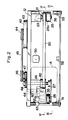
- Figs. 2 to 4 show a mechanical arrangement of the IC card reader/writer.
- An inserting port assembly 11 is provided in a part (at the left end in the diagram) of a frame 10 of the IC card reader/writer.
- An IC card inserting port 12 is opened in the front edge portion of the assembly 11.
- a short card-guide path 13 is provided in the assembly 11 from the inserting port 12 toward the frame 10.
- a sensor to detect whether the inserted card is a predetermined card or not on the basis of the width of the inserted card, a sensor to check whether data has been recorded on a magnetic stripe of the card or not, and the like are provided on the guide path 13. If the inserted card is determined to be a normal card by those sensors, a shutter, which will be explained hereinafter, is opened.
- the card conveying apparatus includes an upper conveying belt 20 and a lower conveying belt 30.
- the belts 20 and 30 are provided at the almost central position in the width direction of the frame 10.
- the upper conveying belt 20 is reeved around pulleys 21 and 22.
- the lower conveying belt 30 is reeved around pulleys 31 and 32.
- the pulley 21 is rotatably attached to a shaft 23 fixed to the frame 10.
- the pulley 22 is fixed to a rotating shaft 24 which is rotatably supported to the frame 10.
- the pulley 31 is rotatably attached to a shaft 33 fixed to the frame 10.
- the pulley 32 is fixed to a rotating shaft 34 which is rotatably supported to the frame 10.
- a small pulley 41 is fixed to an output shaft of a drive motor 40 fixed to the frame 10.
- a large pulley 43 and a middle pulley 44 are fixed to the rotating shaft 34 on the outside of the frame 10.
- a belt 42 is reeved around the pulleys 41 and 43. Therefore, the lower conveying belt 30 is driven by the drive motor 40 through the pulley 41, belt 42, pulley 43, rotating shaft 34 and pulley 32.
- a rotating shaft 49 is rotatably supported to the outside of the frame 10.
- a pulley 46 and a gear 47 are fixed to the rotating shaft 49.
- a belt 45 is reeved between the pulleys 46 and 44.
- a gear 48 is fixed to the rotating shaft 24. The gear 48 is come into engagement with the gear 47. Therefore, the upper conveying belt 20 is driven by the drive motor 40 synchronously with the lower conveying belt 30 through the rotating shaft 34, pulley 44, belt 45, pulley 46, rotating shaft 49, gear 47, gear 48, rotating shaft 24, and pulley 22.
- the IC card is sandwiched between the upper and lower conveying belts 20 and 30 and conveyed.
- the IC card By switching the forward/reverse rotation of the drive motor 40, the IC card can be conveyed from one end, i.e., the side of the inserting port 12 of the frame 10 toward the other end of the frame 10 (in the carrying-in direction) and in the opposite direction (ejecting direction).
- the upper and lower conveying belts 20 and 30 are arranged so as to be deviated from each other in the conveying direction of the IC card.
- a space 54 is formed over the lower conveying belt 30 in the central portion in the width direction of the frame 10.
- a space 55 is formed below the upper conveying belt 20 in the central portion in the width direction of the frame 10.
- a connector having a plurality of contact members, adapted to be respectively come into contact with the contacts of the contact portion of the IC card can be arranged in the spaces 54 and 55, as will be explained hereinlater.
- the holding means comprises a receiving roller and pressing roller.
- a receiving roller 35 and a pressing roller 26 are provided on the side of the space portion 54.
- the receiving roller 35 is rotatably supported to the shaft 33 and rotates together with the pulley 31 by being coupled with the pulley 31 by a pin (not shown).
- the pressing roller 26 is rotatably attached to a free end portion of a lever 27 which is rotatably supported to the rotating shaft 24. The lever 27 is pressed by a spring (not shown), so that the pressing roller 26 is come into pressure contact with the receiving roller 35.
- a receiving roller 25 and a pressing roller 36 are provided on the side of the space portion 55.
- the receiving roller 25 is rotatably attached to the shaft 23 and is rotated together with the pulley 21 by being coupled with the pulley 21 by a pin 25a.
- the pressing roller 36 is rotatably attached to a free end portion of a lever 37 which is rotatably attached to the rotating shaft 34. Since the lever 37 is pressed by a spring (not shown), the pressing roller 36 is come into pressure contact with the receiving roller 25.
- a connector 60 is provided in only the space portion 54 near the card inserting port 12.
- the connector 60 holds a plurality of contact members 61 so as to be mutually isolated.
- the connector 60 is attached and fixed to a swing supporting plate 62 and the contact members 61 are directed to the lower conveying belt 30.
- the swing supporting plate 62 has a lever portion 65 extending downwardly from one end portion thereof. At a proper portion of the lever portion 65, the swing supporting plate 62 is swingably supported by a fulcrum shaft 64 fixed to the frame 10.
- a leading portion 63 serving as a shutter is integrally formed in the front edge portion of the swing supporting plate 62.
- the swing supporting plate 62 is driven by a solenoid 69 attached to the frame 10.
- the swing supporting plate 62 When the IC card is held and positioned at a predetermined location between the upper conveying belt 20 and pressing roller 26, and the lower conveying belt 30 and receiving roller 35, the swing supporting plate 62 is held to an attitude indicated by a solid line in Fig. 4. At this time, the contact members 61 of the connector 60 are come into contact with the contacts of the positioned IC card and at the same time, the leading portion 63 shuts off the passage between the card inserting port 12 and the conveying path between both of the upper and lower conveying belts 20 and 30 (the shutter is closed). Further, a part of the lever 65 is detected by a sensor 68. On the basis of a detection signal of the sensor 68, it is confirmed that the connector 60 is in contact with the IC card.
- the connector 60 When the supporting plate 62 obliquely rises by the actuation of the solenoid 69 as shown by an alternate long and short dash line in Fig. 4, the connector 60 is away from the IC card. The leading portion 63 is also removed from the conveying path and the shutter is opened.
- a magnetic head 50 is arranged on one side on the way of the conveying path of the IC card and fixed to the frame 10.
- the magnetic head 50 reads out data recorded on the magnetic stripe of the IC card or writes data onto the magnetic stripe.
- a pressing roller is disposed at a position which faces the magnetic head 50. This pressing roller is pressed in the direction of the magnetic head 50.
- first, second and third sensors 51, 52 and 53 to detect the IC card which is conveyed by the conveying apparatus are attached to one end, a central position and the other end in the card conveying direction of the frame 10, respectively.
- Fig. 5 shows an outline of an electrical arrangement of the IC card reader/writer.
- the IC card reader/writer includes a CPU 80.
- the CPU 80 has an ROM 81 in which a program is stored and an RAM 82 to store various data.
- the first to third sensors 51 to 53, sensor 68, connector 60, motor 40 and solenoid 69 are connected to the CPU 80 through proper interfaces, respectively.
- the CPU 80 controls the motor 40 and solenoid 69 on the basis of detection signals from the sensors 51 to 53 and the other sensors.
- the CPU 80 performs the reading/writing processes to write the data of the RAM 82 into the IC card and to store the data read out of the IC card into the RAM 82 through the connector 60.
- IC cards A1, A3, and A4 (hereinafter, the IC card is simply indicated at reference character A) of the USA format and JPN format.
- the IC card of the USA format the back surface of the card faces upward and the card is inserted from the inserting port 12.
- the upper surface faces upward and the card is inserted from the inserting port 12.
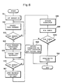
- the card conveying apparatus driven by the motor 40 conveys the IC card A in the forward direction, that is, in the carrying-in direction (steps S11 and S12).
- the IC card In the case where data is read out from or written onto the magnetic stripe of the IC card A by the magnetic head 50, the IC card is conveyed in the forward direction until the IC card A is detected by the third sensor 53 and the reading/writing operation may be performed by the magnetic head 50 in this conveying step. Thereafter, the IC card A is conveyed in the opposite direction until the IC card is detected by the first sensor 51.
- step S16 and S17 When the first sonsor 51 again detects the card due to the conveyance of the IC card A in the ejecting (returning) direction, the conveyance of the card is stopped (steps S16 and S17).
- the swing supporting plate 62 is rotated to the horizontal attitude shown by a solid line in Fig. 4 by the solenoid 69.
- the shutter on the card inserting port side is closed and the connector 60 is come into contact with the contact portion C of the IC card A (step S18).
- a pin check is executed (step S20).
- the pin check relates to that the CPU 80 executes the transmission and reception of check data with the IC card through the contact members 61 of the connector 60. If the transmission and reception of the check data are correctly performed, the pin check is OK.
- information is transmitted and received between the IC card A and the CPU 80 through the contact between the contact members 61 of the connector 60 and the contacts of the contact portion C of the IC card A. That is, data is read out from and writen into the IC card A.
- the connector 60 is returned to the idle position and the motor 40 is reversely rotated, thereby returning the IC card to the card inserting port 12 (step S22).
- the shutter is commonly used as a supporting plate of the connector, the number of parts can be reduced, the driving mechanism can be simplified, and the IC card reader/writer can be miniaturized.
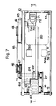
- Figs. 7 and 8 show another embodiment.
- the IC card reader/writer in this embodiment enables the reading/writing operations of an IC card of the BULL format as well as the USA and JPN formats.
- Figs. 7 and 8 the same parts and components as those shown in Figs. 2 to 4 are designated by the same reference numerals.
- a swing supporting plate 72 is also provided in the space 55 and a connector 70 having contact members 71 is attached and fixed to the supporting plate 72.
- the supporting plate 72 and connector 70 are arranged at positions which are slightly deviated to the side so as to correspond to the contact portion C2 of the IC card A2 of the BULL format.
- the connector 70 faces upwardly.
- the supporting plate 72 has a lever portion 75 and is pivotally attached to a shaft 74.
- a sensor 78 to detect the contact position of the connector 70 to the contact portion is provided.
- the supporting plate 72 is driven by a solenoid 79.
- the supporting plate 72 is not provided with a portion serving as a shutter.
- the senor 78 is connected to the CPU 80 and a solenoid 79 is controlled by the CPU 80.
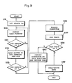
- the IC card of the BULL format is inserted into the inserting port 12 in a state in which the back surface faces upward. The operation at this time will now be described with reference to Fig. 9.
- the card conveying apparatus conveys the IC card A by the motor 40 in the forward direction, namely, in the inserting direction.
- the shutter at the position of the card inserting port 12 is open (that is, the supporting plate 62 is located at the idle position).
- the supporting plate 72 and connector 70 are also located at the idle position (steps S31 and S32).
- the shutter i.e., the supporting plate 62
- the conveying path is shut off (the shutter is closed) by the leading portion 63, thereby closing the card inserting port (steps S33 and S34).
- the reading/writing process of the magnetic stripe is executed by the magnetic head 50 during the conveyance of the IC card.
- the pin check is then performed. If the result of the pin check is OK, the reading/writing operation of the IC data is executed and the processing routine is finished (steps S38 and S39). If the result of the pin check is NG, the supporting plates 62 and 72 are returned to the idle position, the motor 40 is reversely rotated, the IC card is returned, and the processing routine is finished (step S40).
- the shutter (leading portion 63) closes the card inserting port 12, thereby blocking that the IC card in the IC card reader is moved or pulled out due to the insertion of foreign matter or card from the card inserting port.
- another connector can be also further arranged in the space 55 at the position for use of the card of the USA or JPN format.
- an inserting port assembly 11A can be also provided in the edge portion of the frame 10 on the side of the space 55.
- a leading portion serving as a shutter is also provided for the supporting plate 72.
- another magnetic head may be also arranged.
- the card reader/writer can be limited to the data process of the IC card of the USA or JPN format. If the connector 60 and supporting plate 62 are eliminated, the card reader/writer can be limited to the data process of the IC card of the BULL format. If the connectors 70 and 60 are eliminated, the card reader/writer can be used as only a reader/writer of the magnetic card.
- the card reader/writer can be used as the reader/writer of the IC card having no magnetic stripe.
Landscapes
- Engineering & Computer Science (AREA)
- Physics & Mathematics (AREA)
- General Physics & Mathematics (AREA)
- Theoretical Computer Science (AREA)
- Artificial Intelligence (AREA)
- Computer Vision & Pattern Recognition (AREA)
- Conveying Record Carriers (AREA)
Claims (2)
- Un dispositif de lecture/écriture de cartes à circuit intégré comprenant un appareil de transport d'une carte à circuit intégré, prévu pour faire entrer un carte à circuit intégré insérée dans un orifice d'insertion (12) de carte du dispositif de lecture/écriture de cartes à circuit intégré et pour faire sortir vers l'orifice d'insertion de carte la carte à circuit intégré située à l'intérieur, et un connecteur (60, 70) pourvu d'organes de contact (61, 71) aptes à venir en contact avec des contacts de la carte à circuit intégré transportée par l'appareil de transport vers une position prédéterminée dans le dispositif de lecture/écriture de cartes à circuit intégré, ledit appareil de transport de carte incluant une courroie transporteuse supérieure (20) passant autour de poulies (21, 22) et une courroie transporteuse inférieure (30) passant autour de poulies (31, 32), lesdites courroies transporteuses supérieure et inférieure étant d'une longueur sensiblement égale dans la direction de transport de la carte et transportant la carte à circuit intégré en la prenant en sandwich
caractérisé en ce que
lesdites courroies transporteuses supérieure et inférieure (20, 30) sont décalées longitudinalement dans la direction de transport de la carte afin de former des espaces (54, 55) susceptibles de loger un tel connecteur (60, 70) au moins à chaque extrémité de la paire de courroies, et
un moyen (25, 26, 35, 36) de maintien de la carte à circuit intégré est disposé auxdits espaces. - Un dispositif de lecture/écriture de cartes à circuit intégré selon la revendication 1, caractérisé en ce que le connecteur (60), qui est disposé dans l'espace voisin de l'orifice d'insertion (12) est attaché à un organe d'un volet (62, 63) d'ouverture et de fermeture de l'orifice d'insertion (12) de carte.
Priority Applications (1)
| Application Number | Priority Date | Filing Date | Title |
|---|---|---|---|
| AT88116687T ATE85855T1 (de) | 1987-10-09 | 1988-10-07 | Lese-/schreibgeraet fuer eine ic-karte. |
Applications Claiming Priority (4)
| Application Number | Priority Date | Filing Date | Title |
|---|---|---|---|
| JP1987155056U JPH0161764U (fr) | 1987-10-09 | 1987-10-09 | |
| JP155056/87U | 1987-10-09 | ||
| JP158143/87U | 1987-10-15 | ||
| JP1987158143U JPH0716201Y2 (ja) | 1987-10-15 | 1987-10-15 | カードリーダライタ |
Publications (2)
| Publication Number | Publication Date |
|---|---|
| EP0311119A1 EP0311119A1 (fr) | 1989-04-12 |
| EP0311119B1 true EP0311119B1 (fr) | 1993-02-17 |
Family
ID=26483161
Family Applications (1)
| Application Number | Title | Priority Date | Filing Date |
|---|---|---|---|
| EP88116687A Expired - Lifetime EP0311119B1 (fr) | 1987-10-09 | 1988-10-07 | Dispositif de lecture/écriture d'une carte à circuit intégré |
Country Status (5)
| Country | Link |
|---|---|
| US (1) | US4871905A (fr) |
| EP (1) | EP0311119B1 (fr) |
| CA (1) | CA1323927C (fr) |
| DE (1) | DE3878524T2 (fr) |
| ES (1) | ES2039543T3 (fr) |
Families Citing this family (22)
| Publication number | Priority date | Publication date | Assignee | Title |
|---|---|---|---|---|
| US5189661A (en) * | 1988-12-27 | 1993-02-23 | Kabushiki Kaisha | Card carrier |
| DE8906634U1 (fr) * | 1989-05-30 | 1989-07-20 | Siemens Ag, 1000 Berlin Und 8000 Muenchen, De | |
| US5309176A (en) * | 1992-08-25 | 1994-05-03 | Sci Systems, Inc. | Airline ticket printer with stepper motor for selectively engaging print head and platen |
| US5332889A (en) * | 1992-12-18 | 1994-07-26 | Datacard Corporation | Integrated circuit card programming device |
| JPH07254206A (ja) * | 1994-03-16 | 1995-10-03 | Nec Eng Ltd | カートリッジアクセスステーション |
| US5646392A (en) * | 1994-06-13 | 1997-07-08 | Sankyo Seiki Mfg. Co., Ltd. | Card reader |
| US6068187A (en) * | 1994-10-18 | 2000-05-30 | Seiko Epson Corporation | Information detection apparatus and information detection method for recording media |
| TW293899B (fr) * | 1994-10-18 | 1996-12-21 | Seiko Epson Corp | |
| US5965862A (en) * | 1994-10-18 | 1999-10-12 | Seiko Epson Corporation | Information detection apparatus and method for printing on a medium and for reading information recorded on the medium |
| JPH09245129A (ja) * | 1996-03-06 | 1997-09-19 | Nippon Conlux Co Ltd | カード搬送制御方法および装置 |
| JPH10105665A (ja) * | 1996-09-30 | 1998-04-24 | Hitachi Ltd | Icカード用端末装置 |
| NL1007956C2 (nl) * | 1998-01-05 | 1999-08-25 | Lumino B V | Doorschuifchipkaartlezer. |
| JP3367039B2 (ja) * | 1998-01-09 | 2003-01-14 | アンリツ株式会社 | Icカード処理装置 |
| FR2777099A1 (fr) * | 1998-04-01 | 1999-10-08 | Hubert Calvados | Support portant des moyens de codage permettant son authentification ainsi que dispositif de relecture d'un tel support |
| TW426630B (en) | 1998-05-28 | 2001-03-21 | Asahi Seiko Co Ltd | IC card processing machine |
| US6659348B2 (en) * | 2000-01-24 | 2003-12-09 | Sankyo Seiki Mfg. Co., Ltd. | Manual IC card reader and manual card reader |
| JP3907934B2 (ja) * | 2000-09-20 | 2007-04-18 | 日本電産サンキョー株式会社 | 手動式icカードリーダ |
| DE10160276A1 (de) * | 2001-12-07 | 2003-06-26 | Siemens Ag | Antriebsanordnung für wenigstens ein in einem Fahrtschreiber angeordnetes Chipkarten-Aufnahmeaggregat zum Verbringen einer Chipkarte in die Entnahmeposition |
| DE10321251A1 (de) * | 2003-05-12 | 2004-12-09 | Siemens Ag | Kartenaufnahmevorrichtung und Verfahren |
| JP4518756B2 (ja) * | 2003-08-11 | 2010-08-04 | 日立オムロンターミナルソリューションズ株式会社 | カード情報読み取り装置およびicカードリーダ |
| JP4064913B2 (ja) * | 2003-12-02 | 2008-03-19 | 日本電産サンキョー株式会社 | カードリーダ |
| JP4667919B2 (ja) * | 2005-03-17 | 2011-04-13 | 日立オムロンターミナルソリューションズ株式会社 | カード読取書込装置 |
Family Cites Families (4)
| Publication number | Priority date | Publication date | Assignee | Title |
|---|---|---|---|---|
| FR2477303B1 (fr) * | 1980-02-28 | 1986-09-26 | Dassault Electronique | Dispositif de lecture de cartes electroniques |
| GB2170165A (en) * | 1985-01-30 | 1986-07-30 | Cubic Western Data | Ticket transport mechanism |
| FR2587131B1 (fr) * | 1985-09-12 | 1987-11-20 | Bull Transac | Lecteur encodeur de carte d'identification |
| FR2592193B1 (fr) * | 1985-09-20 | 1988-07-22 | Michot Gerard | Lecteur pour support d'informations electroniques |
-
1988
- 1988-10-04 US US07/252,930 patent/US4871905A/en not_active Expired - Lifetime
- 1988-10-07 ES ES198888116687T patent/ES2039543T3/es not_active Expired - Lifetime
- 1988-10-07 CA CA000579555A patent/CA1323927C/fr not_active Expired - Lifetime
- 1988-10-07 DE DE8888116687T patent/DE3878524T2/de not_active Expired - Lifetime
- 1988-10-07 EP EP88116687A patent/EP0311119B1/fr not_active Expired - Lifetime
Also Published As
| Publication number | Publication date |
|---|---|
| US4871905A (en) | 1989-10-03 |
| ES2039543T3 (es) | 1993-10-01 |
| DE3878524D1 (de) | 1993-03-25 |
| CA1323927C (fr) | 1993-11-02 |
| DE3878524T2 (de) | 1993-09-16 |
| EP0311119A1 (fr) | 1989-04-12 |
Similar Documents
| Publication | Publication Date | Title |
|---|---|---|
| US5010239A (en) | IC card reader/writer | |
| EP0311119B1 (fr) | Dispositif de lecture/écriture d'une carte à circuit intégré | |
| EP0399763B1 (fr) | Dispositif de lecture et d'écriture d'une carte à circuit intégré | |
| EP0712087B1 (fr) | Lecteur de carte | |
| US5917177A (en) | IC card reader | |
| JP4075754B2 (ja) | 非接触式通信媒体挿入口モジュール | |
| JPWO2009122715A1 (ja) | カードリーダ及びその処理方法 | |
| EP1830302B1 (fr) | Lecteur de cartes | |
| EP0837414B1 (fr) | Capteur de cartes magnétiques | |
| US4861974A (en) | Card reader | |
| EP0492358A1 (fr) | Terminal électronique et méthode de codage de cartes à piste magnétique ou cartes à C.I. | |
| US4138059A (en) | Card handling device | |
| US20040050938A1 (en) | Card connector | |
| EP1115084B1 (fr) | Mécanisme de bloc de contacts pour lecteur de carte à puce | |
| JP2020042396A (ja) | カードリーダ及びカードリーダ制御方法 | |
| CN110619246B (zh) | 读卡器及异物检测方法 | |
| US8056811B2 (en) | Anti-misinsertion mechanism of card connector | |
| KR100579403B1 (ko) | Ic카드인식기능이 구비된 마그네틱 스트라이프 카드로딩장치 | |
| JP7085932B2 (ja) | カードリーダ | |
| WO2024058069A1 (fr) | Procédé de positionnement de carte et lecteur de carte | |
| JP3082698B2 (ja) | カードリーダ | |
| KR200398965Y1 (ko) | 카드리더기용 셔터장치 | |
| JPS6310502B2 (fr) | ||
| JPH0322095A (ja) | カードリーダライタ | |
| JPH01219973A (ja) | Icカードの取り出し防止装置 |
Legal Events
| Date | Code | Title | Description |
|---|---|---|---|
| PUAI | Public reference made under article 153(3) epc to a published international application that has entered the european phase |
Free format text: ORIGINAL CODE: 0009012 |
|
| 17P | Request for examination filed |
Effective date: 19881007 |
|
| AK | Designated contracting states |
Kind code of ref document: A1 Designated state(s): AT BE CH DE ES FR GB GR IT LI LU NL SE |
|
| 17Q | First examination report despatched |
Effective date: 19910110 |
|
| GRAA | (expected) grant |
Free format text: ORIGINAL CODE: 0009210 |
|
| AK | Designated contracting states |
Kind code of ref document: B1 Designated state(s): AT BE CH DE ES FR GB GR IT LI LU NL SE |
|
| PG25 | Lapsed in a contracting state [announced via postgrant information from national office to epo] |
Ref country code: SE Effective date: 19930217 Ref country code: NL Effective date: 19930217 Ref country code: GR Free format text: LAPSE BECAUSE OF FAILURE TO SUBMIT A TRANSLATION OF THE DESCRIPTION OR TO PAY THE FEE WITHIN THE PRESCRIBED TIME-LIMIT Effective date: 19930217 Ref country code: BE Effective date: 19930217 Ref country code: CH Effective date: 19930217 Ref country code: LI Effective date: 19930217 Ref country code: AT Effective date: 19930217 |
|
| REF | Corresponds to: |
Ref document number: 85855 Country of ref document: AT Date of ref document: 19930315 Kind code of ref document: T |
|
| ITF | It: translation for a ep patent filed |
Owner name: STUDIO TORTA SOCIETA' SEMPLICE |
|
| REF | Corresponds to: |
Ref document number: 3878524 Country of ref document: DE Date of ref document: 19930325 |
|
| ET | Fr: translation filed | ||
| REG | Reference to a national code |
Ref country code: CH Ref legal event code: PL |
|
| NLV1 | Nl: lapsed or annulled due to failure to fulfill the requirements of art. 29p and 29m of the patents act | ||
| REG | Reference to a national code |
Ref country code: ES Ref legal event code: FG2A Ref document number: 2039543 Country of ref document: ES Kind code of ref document: T3 |
|
| PG25 | Lapsed in a contracting state [announced via postgrant information from national office to epo] |
Ref country code: LU Free format text: LAPSE BECAUSE OF NON-PAYMENT OF DUE FEES Effective date: 19931031 |
|
| PLBE | No opposition filed within time limit |
Free format text: ORIGINAL CODE: 0009261 |
|
| STAA | Information on the status of an ep patent application or granted ep patent |
Free format text: STATUS: NO OPPOSITION FILED WITHIN TIME LIMIT |
|
| 26N | No opposition filed | ||
| PGFP | Annual fee paid to national office [announced via postgrant information from national office to epo] |
Ref country code: ES Payment date: 19961007 Year of fee payment: 9 |
|
| PG25 | Lapsed in a contracting state [announced via postgrant information from national office to epo] |
Ref country code: ES Free format text: LAPSE BECAUSE OF EXPIRATION OF PROTECTION Effective date: 19971008 |
|
| REG | Reference to a national code |
Ref country code: GB Ref legal event code: 746 Effective date: 20000503 |
|
| REG | Reference to a national code |
Ref country code: FR Ref legal event code: D6 |
|
| REG | Reference to a national code |
Ref country code: ES Ref legal event code: FD2A Effective date: 20010201 |
|
| REG | Reference to a national code |
Ref country code: GB Ref legal event code: IF02 |
|
| PG25 | Lapsed in a contracting state [announced via postgrant information from national office to epo] |
Ref country code: IT Free format text: LAPSE BECAUSE OF NON-PAYMENT OF DUE FEES Effective date: 20051007 |
|
| REG | Reference to a national code |
Ref country code: GB Ref legal event code: 732E |
|
| PG25 | Lapsed in a contracting state [announced via postgrant information from national office to epo] |
Ref country code: FR Free format text: LAPSE BECAUSE OF NON-PAYMENT OF DUE FEES Effective date: 20060630 |
|
| REG | Reference to a national code |
Ref country code: FR Ref legal event code: ST Effective date: 20060630 |
|
| REG | Reference to a national code |
Ref country code: FR Ref legal event code: D3 |
|
| PGFP | Annual fee paid to national office [announced via postgrant information from national office to epo] |
Ref country code: DE Payment date: 20071031 Year of fee payment: 20 |
|
| PGFP | Annual fee paid to national office [announced via postgrant information from national office to epo] |
Ref country code: FR Payment date: 20071015 Year of fee payment: 20 Ref country code: GB Payment date: 20071012 Year of fee payment: 20 |
|
| REG | Reference to a national code |
Ref country code: GB Ref legal event code: PE20 Expiry date: 20081006 |
|
| PG25 | Lapsed in a contracting state [announced via postgrant information from national office to epo] |
Ref country code: GB Free format text: LAPSE BECAUSE OF EXPIRATION OF PROTECTION Effective date: 20081006 |
|
| PGFP | Annual fee paid to national office [announced via postgrant information from national office to epo] |
Ref country code: IT Payment date: 20071031 Year of fee payment: 20 |
|
| PGRI | Patent reinstated in contracting state [announced from national office to epo] |
Ref country code: IT Effective date: 20091201 |