EP0309922B1 - Schaltung zur kurzzeitigen Erhöhung einer geregelten Betriebsspannung beim Einschalten und bei Spannungseinbrüchen - Google Patents
Schaltung zur kurzzeitigen Erhöhung einer geregelten Betriebsspannung beim Einschalten und bei Spannungseinbrüchen Download PDFInfo
- Publication number
- EP0309922B1 EP0309922B1 EP88115591A EP88115591A EP0309922B1 EP 0309922 B1 EP0309922 B1 EP 0309922B1 EP 88115591 A EP88115591 A EP 88115591A EP 88115591 A EP88115591 A EP 88115591A EP 0309922 B1 EP0309922 B1 EP 0309922B1
- Authority
- EP
- European Patent Office
- Prior art keywords
- voltage
- voltage regulator
- capacitor
- output
- switching
- Prior art date
- Legal status (The legal status is an assumption and is not a legal conclusion. Google has not performed a legal analysis and makes no representation as to the accuracy of the status listed.)
- Expired - Lifetime
Links
- 230000001105 regulatory effect Effects 0.000 title claims description 3
- 239000003990 capacitor Substances 0.000 claims description 26
- 230000006870 function Effects 0.000 description 2
- 230000010355 oscillation Effects 0.000 description 2
- 230000015556 catabolic process Effects 0.000 description 1
- 239000013078 crystal Substances 0.000 description 1
- 238000011161 development Methods 0.000 description 1
- 230000018109 developmental process Effects 0.000 description 1
- 238000010586 diagram Methods 0.000 description 1
- 230000005669 field effect Effects 0.000 description 1
- 238000000034 method Methods 0.000 description 1
- 238000011144 upstream manufacturing Methods 0.000 description 1
Images

Classifications
-
- G—PHYSICS
- G05—CONTROLLING; REGULATING
- G05F—SYSTEMS FOR REGULATING ELECTRIC OR MAGNETIC VARIABLES
- G05F1/00—Automatic systems in which deviations of an electric quantity from one or more predetermined values are detected at the output of the system and fed back to a device within the system to restore the detected quantity to its predetermined value or values, i.e. retroactive systems
- G05F1/10—Regulating voltage or current
- G05F1/46—Regulating voltage or current wherein the variable actually regulated by the final control device is DC
- G05F1/56—Regulating voltage or current wherein the variable actually regulated by the final control device is DC using semiconductor devices in series with the load as final control devices
- G05F1/565—Regulating voltage or current wherein the variable actually regulated by the final control device is DC using semiconductor devices in series with the load as final control devices sensing a condition of the system or its load in addition to means responsive to deviations in the output of the system, e.g. current, voltage, power factor
Definitions
- the invention relates to a voltage regulator for a brief increase when switching on and in the event of voltage dips, a regulated supply voltage of a gunnoscillator.
- the invention has for its object to provide a voltage regulator with which the above problems are solved, i. H. the voltage reserve for safe start-up at low temperatures and / or limited operating voltage is increased, the susceptibility to vibration of gunn oscillators at the undesired higher frequencies and the power loss of a tunnel element are reduced and its service life is increased.
- a voltage regulator which contains a circuit to which a timing element is connected in parallel on the input side, the output signal of which is fed to a switching element, and which also contains a capacitor between the switching element and the output of the circuit in order to achieve the desired voltage increase, the capacitor voltage being superimposed as a voltage peak shifted by an adjustable time on the switching element of the output voltage of the voltage regulator.
- the difference between the Gunn operating and starting voltage is significantly increased, and thereby the oscillation of the oscillator particularly safer at low temperatures.
- the gun diode can thus be operated at a reduced voltage.
- the Gunn voltage settles after switching on, the operating range of a gun diode coming from high frequencies passes through a large frequency range. A latching of the gun diode on unwanted resonance points is avoided by such a brief increase in the Gunn voltage, so that the working range of the diode is below the target frequency.
- the circuit contains a voltage regulator 1 in the series branch which the input voltage Ue is applied as the operating voltage.
- the output voltage of the voltage regulator 1 is denoted by Ua, behind a choke Dr lying in the output circuit of the voltage regulator with Ua '.
- a parallel line branch is connected on the input side to the voltage regulator 1 and contains a timing element with a comparator 2 and a switching element consisting of a transistor Tr and connected to its output.
- the comparator has two inputs X and Y.
- Input X is connected to the connection point of a voltage divider connected to the operating voltage from a resistor R2 and a Zener diode D1
- input Y is connected to the connection point of a voltage divider connected to the operating voltage from a resistor R1 and one Capacitor C4.
- a diode D3 is also switched on between this connection point and the operating voltage source (shown in broken lines).
- the comparator output is connected via a capacitor C to the gate terminal of the switching element consisting of a field effect transistor Tr. Whose drain connection is led to the output of the voltage regulator 1 in front of the choke.
- a capacitor C3 connected to the source terminal of the transistor Tr is connected to the output of the voltage regulator 1 located behind the inductor Dr and via a diode D2 to the drain terminal and thus also to the output of the voltage regulator 1 located in front of the inductor Dr .
- a shunt arm with a capacitor C1 and C2 is connected to the output of the voltage regulator 1 in front of and behind the choke Dr.
- the resistor R lying in parallel with the inductor Dr and shown in broken lines can be switched into the discharge circuit of the capacitor C3 instead of the inductor Dr.
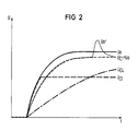
- the operating voltage (input voltage Ue) present at the input of the voltage regulator 1 has the profile shown in FIG. 2, namely after the switch-on process it reaches the end value within a certain time after an approximately e-function profile.
- the capacitors C1 in the output-side transverse branch of the voltage regulator 1 and C3 in the source circuit of the transistor Tr are charged to the output voltage Ua.
- the capacitor C1 as a memory at the output of the voltage regulator 1 is provided in order to avoid a reduction in the amplitude of the desired voltage peak by the voltage regulator.
- the voltage Ua at the output of the voltage regulator upstream of the choke, which corresponds to the voltage at the capacitor C1 is lower than the input voltage Ue, as can be seen in FIG. 2.
- This superposition of the two voltages occurs when, after the same input voltages have been reached at the inputs X and Y of the comparator 2, ie if the voltages U C4 and U D1 are the same, the comparator 2 controls the transistor Tr in such a way that it is switched to the open position.
- the transistor can of course also be replaced by a corresponding element with a switch function, for example a relay.
- the breakdown voltage of the Zener diode D1 is selected so that it is less than the input voltage Ue and greater than the voltage which leads to the vibration breaking off when the Gunn supply voltage is reduced.
- a time must be set until the switching threshold of the comparator is reached, which is greater than the charging time of the capacitors C3 and C1. So that will ensures that the capacitors C3 and C1 are already charged before the comparator output turns on the transistor and the voltage U C3 of the capacitor C3 is superimposed on the output voltage Ua on the capacitor C1.
- the amplitude of the voltage peak can be set by varying the capacitance values of the capacitors C1, C2 and C3.
- the diode D3 between the connection point of the voltage divider R1 / C4 and the circuit input is used to quickly discharge the capacitor C4 when the supply voltage Ue drops. This ensures that a defined switch-on time for the supply voltage is reached again.
- the circuit described above is implemented with a voltage regulator, the regulator being an expression for a stable voltage of a voltage source. What is essential, however, is only the fact that a stable voltage is briefly applied a second voltage via a corresponding time element.
Landscapes
- Engineering & Computer Science (AREA)
- Physics & Mathematics (AREA)
- Electromagnetism (AREA)
- General Physics & Mathematics (AREA)
- Radar, Positioning & Navigation (AREA)
- Automation & Control Theory (AREA)
- Dc-Dc Converters (AREA)
Description
- Die Erfindung bezieht sich auf einen Spannungsregler zur kurzzeitigen Erhöhung beim Einschalten und bei Spannungseinbrüchen, einer geregelten Versorgungsspannung eines Gunnoszillators.
- Gunnoszillatoren besitzen die Anfälligkeit, bei höheren, nicht gewünschten Frequenzen zu schwingen. Es ist eine bestimmte Spannungsreserve zum sicheren Anschwingen bei tiefen Temperaturen erforderlich. Eine entsprechend hohe Spannung erhöht jedoch die Verlustleistung des Gunnelements, was zugleich zu einer Verminderung seiner Lebensdauer führt.
- Der Erfindung liegt die Aufgabe zugrunde, einen Spannungsregler zu schaffen, mit der die vorstehend genannten Probleme gelöst werden, d. h. die Spannungsreserve zum sicheren Anschwingen bei tiefen Temperaturen und/oder begrenzter Betriebsspannung erhöht, die Schwinganfälligkeit von Gunnoszillatoren bei den unerwünschten höheren Frequenzen und die Verlustleistung eines Gunnelements reduziert sowie seine Lebensdauer erhöht werden.
- Diese Aufgabe wird gemäß der Erfindung mit einem Spannungsregler gelöst, der eine Schaltung enthält, zu dem eingangsseitig ein Zeitglied parallel angeschaltet ist, dessen Ausgangssignal einem Schaltelement zugeführt wird, und die ferner einen Kondensator zwischen Schaltelement und Ausgang der Schaltung enthält zur Erzielung der gewünschten Spannungserhöhung, wobei die Kondensator-Spannung als eine um eine einstellbare Zeit verschobene Spannungsspitze über das Schaltelement der Ausgangsspannung des Spannungsreglers überlagert wird.
- Bei Verwendung der erfindungsgemäßen Schaltung für einen Gunnoszillator, die nach dem Einschalten der Gunnversorgungsspannung eine um eine einstellbare Zeit verschobene, in ihrer Höhe innerhalb bestimmter Grenzen wählbare Spannungsspitze erzeugt, wird die Differenz zwischen der Gunnbetriebs- und Anschwingspannung deutlich erhöht und dadurch das Anschwingen des Oszillators besonders bei tiefen Temperaturen sicherer. Die Gunndiode kann somit an einer reduzierten Spannung betrieben werden. Beim Einschwingen der Gunnspannung nach dem Einschalten durchläuft der Arbeitsbereich einer Gunndiode von hohen Frequenzen kommend einen großen Frequenzbereich. Ein Rasten der Gunndiode auf ungewollten Resonanzstellen wird vermieden durch eine solche kurzzeitige Erhöhung der Gunnspannung, so daß der Arbeitsbereich der Diode unterhalb der Sollfrequenz liegt. Damit wird die Anfälligkeit von Gunnoszillatoren, bei höheren, nicht gewünschten Frequenzen zu schwingen, deutlich reduziert, ohne die Nachteile einer konstant höheren Gunnspannung oder der Verwendung einer Gunndiode für tiefere Frequenzen zu erhalten. Ferner wird durch die Möglichkeit, die Gunndiode an einer reduzierten Spannung zu betreiben, die Verlustleistung und damit die Kristalltemperatur gesenkt und die Lebensdauer der Gunndiode erhöht, ohne auf die Spannungsreserve zum Anschwingen zu verzichten.
- Vorteilhafte Ausgestaltungen und Weiterbildungen des Erfindungsgegenstandes sind in den Unteransprüchen angegeben.
- Nachstehend wird die Erfindung anhand eines in der Zeichnung dargestellten Ausführungsbeispiels näher erläutert.
- Es zeigen
- Fig. 1
- eine Schaltung im Blockschaltbild und
- Fig. 2
- in einer grafischen Darstellung den Spannungsverlauf an verschiedenen Punkten der Schaltung.
- Die Schaltung enthält im Längszweig einen Spannungsregler 1, an dem die Eingangsspannung Ue als Betriebsspannung anliegt. Die Ausgangsspannung des Spannungsreglers 1 ist mit Ua bezeichnet, die hinter einer im Ausgangskreis des Spannungsreglers liegenden Drossel Dr mit Ua′. Dem Spannungsregler 1 ist eingangsseitig ein paralleler Leitungszweig angeschaltet, der ein Zeitglied mit einem Komparator 2 und ein an dessen Ausgang angeschaltetes, aus einem Transistor Tr bestehendes Schaltelement enthält. Der Komparator besitzt zwei Eingänge X und Y. Der Eingang X ist mit dem Verbindungspunkt eines an der Betriebsspannung liegenden Spannungsteilers aus einem Widerstand R2 und einer Zenerdiode D1 verbunden, der Eingang Y mit dem Verbindungspunkt eines an der Betriebsspannung liegenden Spannungsteilers aus einem Widerstand R1 und einem Kondensator C4. Zwischen diesem Verbindungspunkt und der Betriebsspannungsquelle ist ferner eine Diode D3 eingeschaltet (strichliert gezeichnet). Der Komparatorausgang ist über einen Kondensator C mit dem Gate-Anschluß des aus einem Feldeffekttransistor Tr bestehenden Schaltelements verbunden. Dessen Drain-Anschluß ist an den vor der Drossel liegenden Ausgang des Spannungsreglers 1 geführt. Ein an den Source-Anschluß des Transistors Tr angeschalteter Kondensator C3 ist mit dem hinter der Drossel Dr liegenden Ausgang des Spannungsreglers 1 und über eine Diode D2 mit dem Drain-Anschluß und damit zugleich auch mit dem vor der Drossel Dr liegenden Ausgang des Spannungsreglers 1 verbunden. An den Ausgang des Spannungsreglers 1 ist vor und hinter der Drossel Dr jeweils ein Querzweig mit einem Kondensator C1 bzw. C2 angeschaltet. Der zur Drossel Dr parallelliegende, strichliert gezeichnete Widerstand R kann anstelle der Drossel Dr in den Entladekreis des Kondensators C3 geschaltet werden.
- Die Funktion dieser Schaltung wird nachstehend unter jeweiliger Berücksichtigung der in Fig. 2 gezeichneten Spannungsverläufe der Eingangs- und Ausgangsspannung Ue, Ua und Ua′ des Spannungsreglers 1 sowie der Spannungen UC4 und UD1 am Kondensator C4 und der Zenerdiode D1 erläutert.
- Die am Eingang des Spannungsreglers 1 anliegende Betriebsspannung (Eingangsspannung Ue) hat den in Fig. 2 gezeigten Verlauf, indem sie nämlich nach dem Einschaltvorgang innerhalb einer bestimmten Zeit nach einem etwa e-Funktionsverlauf den Endwert erreicht. Nach dem Einschwingen des Spannungsreglers 1 sind die Kondensatoren C1 im ausgangsseitige Querzweig des Spannungsreglers 1 und C3 im Sourcekreis des Transistors Tr auf die Ausgangsspannung Ua aufgeladen. Der Kondensator C1 als Speicher am Ausgang des Spannungsreglers 1 ist vorgesehen, um eine Reduzierung der Amplitude der gewünschten Spannungsspitze durch den Spannungsregler zu vermeiden. Die Spannung Ua am Ausgang des Spannungsreglers vor der Drossel, die der Spannung am Kondensator C1 entspricht, ist dabei niedriger als die Eingangsspannung Ue, wie dies aus Fig. 2 erkennbar ist. Der Verlauf der Ausgangsspannung Ua′ am Ausgang des Spannungsreglers hinter der Drossel entspricht im ersten Bereich dem der Spannung am Kondensator C1 (vgl. den strichliert eingezeichneten Spannungsverlauf von Ua′ in Fig. 2) und geht dann in die kurzzeitige Spannungsspitze über, die sich durch die Überlagerung der Spannung an Kondensator C1 mit der am Kondensator C3 ergibt.
- Diese Überlagerung der beiden Spannungen erfolgt dann, wenn nach Erreichen gleicher Eingangsspannungen an den Eingängen X und Y des Komparators 2, d. h. bei Gleichheit der anliegenden Spannungen UC4 und UD1 der Komparator 2 den Transistor Tr so steuert, daß dieser in Durchgangsstellung geschaltet wird. Der Transistor läßt sich selbstverständlich auch durch ein entsprechendes Element mit Schalterfunktion, beispielsweise ein Relais ersetzen. Die Durchbruchspannung der Zenerdiode D1 ist so gewählt, daß sie kleiner ist als die Eingangsspannung Ue und größer als die Spannung, die beim Senken der Gunnversorgungsspannung zum Abriß der Schwingung führt. Mit dem Ohmschen Widerstand R1 und dem Kondensator C4 des Spannungsteilers am Eingang Y des Komparators 2 muß eine Zeit bis zum Erreichen der Schaltschwelle des Komparators eingestellt werden, die größer ist als die Aufladezeit der Kondensatoren C3 und C1. Damit wird sichergestellt, daß die Kondensatoren C3 und C1 bereits aufgeladen sind, bevor der Komparatorausgang den Transistor durchschaltet und sich die Spannung UC3 des Kondensators C3 der Ausgangsspannung Ua am Kondensator C1 überlagert. Durch Variation der Kapazitätswerte der Kondensatoren C1, C2 und C3 läßt sich die Amplitude der Spannungsspitze einstellen. Die Diode D3 zwischen dem Verbindungspunkt des Spannungsteilers R1/C4 und dem Schaltungseingang dient zum schnellen Entladen des Kondensators C4 bei Einbrüchen der Versorgungsspannung Ue. Damit wird erreicht, daß wieder ein definierter Einschaltzeitpunkt für die Versorgungsspannung erreicht wird.
- Die vorstehend beschriebene Schaltung ist mit einem Spannungsregler realisiert, wobei der Regler Ausdruck für eine stabile Spannung einer Spannungsquelle ist. Wesentlich ist dabei jedoch lediglich der Umstand, daß einer stabilen Spannung über ein entsprechendes Zeitelement kurzzeitig eine zweite Spannung aufgeschaltet wird.
Claims (5)
- Spannungsregler zur kurzzeitigen Erhöhung beim Einschalten und bei Spannungseinbrüchen einer geregelten Versorgungsspannung eines Gunnoszillators, dadurch gekennzeichnet, daß dem Spannungsregler (1), eingangsseitig ein Zeitglied (2) parallel angeschaltet ist, dessen Ausgangssignal einem Schaltelement (Tr) zugeführt wird, und daß ferner ein Kondensator (C3) zwischen Schaltelement (Tr) und Ausgang des Spannungsreglers (C1) zur Erzielung der gewünschten Spannungserhöhung vorgesehen ist, wobei die Kondensator-Spannung als eine um eine einstellbare Zeit verschobene Spannungsspitze über das Schaltelement (Tr) der Ausgangsspannung des Spannungsreglers (1) überlagert wird.
- Spannungsregler nach Anspruch 1,
dadurch gekennzeichnet, daß das Zeitglied (2) aus einem Komparator mit zwei Eingängen besteht, an dessen einem Eingang die Teilspannung eines aus einem Widerstand (R1) und einer Kapazität (C4) bestehenden Spannungsteilers und an dessen anderen Eingang eine durch eine Zenerdiode (D1) einstellbare Spannung anliegt und deren bei Spannungsgleichheit gebildetes Ausgangssignal das Schaltelement (Tr) in Durchgangsstellung schaltet. - Spannungsregler nach Anspruch 1 oder 2,
dadurch gekennzeichnet, daß die Zeitkonstante des Zeitgliedes (2) so bemessen ist, daß die Zeit bis zum Erreichen der Schaltschwelle größer ist als die Aufladezeit des Kondensators (C3) zwischen Schaltelement (Tr) und Ausgang des Spannungsreglers (1) sowie eines weiteren Kondensators (C1) am Ausgang des Spannungsreglers. - Spannungsregler nach einem der Ansprüche 1 bis 3,
dadurch gekennzeichnet, daß das Schaltelement (Tr) aus einem Transistor besteht. - Spannungsregler nach einem der Ansprüche 1 bis 4,
dadurch gekennzeichnet, daß zwischen den Verbindungspunkten des Spannungsteilers und die Anschlußklemme der Betriebsspannung eine Diode (D3) eingeschaltet ist.
Applications Claiming Priority (2)
| Application Number | Priority Date | Filing Date | Title |
|---|---|---|---|
| DE3733071 | 1987-09-30 | ||
| DE3733071 | 1987-09-30 |
Publications (3)
| Publication Number | Publication Date |
|---|---|
| EP0309922A2 EP0309922A2 (de) | 1989-04-05 |
| EP0309922A3 EP0309922A3 (en) | 1989-08-02 |
| EP0309922B1 true EP0309922B1 (de) | 1992-12-23 |
Family
ID=6337314
Family Applications (1)
| Application Number | Title | Priority Date | Filing Date |
|---|---|---|---|
| EP88115591A Expired - Lifetime EP0309922B1 (de) | 1987-09-30 | 1988-09-22 | Schaltung zur kurzzeitigen Erhöhung einer geregelten Betriebsspannung beim Einschalten und bei Spannungseinbrüchen |
Country Status (2)
| Country | Link |
|---|---|
| EP (1) | EP0309922B1 (de) |
| DE (1) | DE3876923D1 (de) |
Families Citing this family (1)
| Publication number | Priority date | Publication date | Assignee | Title |
|---|---|---|---|---|
| FR2798480B1 (fr) * | 1999-09-10 | 2001-10-26 | St Microelectronics Sa | Regulateur de tension |
Family Cites Families (1)
| Publication number | Priority date | Publication date | Assignee | Title |
|---|---|---|---|---|
| US3697856A (en) * | 1970-12-14 | 1972-10-10 | Us Navy | Voltage regulating circuit |
-
1988
- 1988-09-22 DE DE8888115591T patent/DE3876923D1/de not_active Expired - Fee Related
- 1988-09-22 EP EP88115591A patent/EP0309922B1/de not_active Expired - Lifetime
Also Published As
| Publication number | Publication date |
|---|---|
| EP0309922A2 (de) | 1989-04-05 |
| EP0309922A3 (en) | 1989-08-02 |
| DE3876923D1 (de) | 1993-02-04 |
Similar Documents
| Publication | Publication Date | Title |
|---|---|---|
| DE69102592T2 (de) | Spannungsgesteuerte ausgeglichene Quarzoszillatorschaltung. | |
| EP0404230A2 (de) | Phasenregelkreis | |
| DE3318536A1 (de) | Durchstimmbare schaltungsanordnung | |
| DE3645149C2 (de) | ||
| DE69500119T2 (de) | Anordnung zum Steuern einer Niederdruckleuchtstofflampe | |
| DE2539632A1 (de) | Kristalloszillator | |
| DE1959162A1 (de) | Digital arbeitender Frequenzgenerator | |
| EP0309922B1 (de) | Schaltung zur kurzzeitigen Erhöhung einer geregelten Betriebsspannung beim Einschalten und bei Spannungseinbrüchen | |
| EP1586183A1 (de) | Oszillatoranordnung f r frequenzmodulation | |
| DE4232026C2 (de) | Elektrostatische Beschichtungspistole und Verfahren zum Erzeugen einer Hochspannung | |
| DE2811080A1 (de) | Durch spannungsaenderung abstimmbarer hochfrequenz-oszillator | |
| DE3751078T2 (de) | Quartz-Oszillator mit breitem Ziehbereich. | |
| DE2557134A1 (de) | Transistoroszillator | |
| DE2001660A1 (de) | Abstimmschaltung fuer eine Vielzahl elektronisch abstimmbarer Schaltkreise | |
| DE3931513A1 (de) | Phasenregelschleife fuer die direktmodulation | |
| EP1526623B1 (de) | Elektrische Schaltung zur Einschaltstrombegrenzung | |
| DE3124492C2 (de) | ||
| EP0361353B1 (de) | Gleichstromgespeiste Steuerschaltung für ein Magnetventil | |
| DE1766840C (de) | Amplitudengeregelter Generator | |
| DE19535695C2 (de) | Spannungsgesteuerter Oszillator | |
| DE2701353A1 (de) | Mischstufe mit kapazitiver einkopplung der oszillatorfrequenz | |
| EP0759657A1 (de) | Verfahren zur Resonanzkreisabstimmung durch Veränderung der Speisespannung einer Kapazitätsdiode | |
| DE3930751A1 (de) | Schaltungsanordnung zur taktrueckgewinnung | |
| EP1515443B1 (de) | Frequenzstabilisierung eines als niederfrequenter Taktgeber in Mobilfunkgeräten verwendeten stromgesteuerten Oszillatorschaltkreises | |
| DE2929897A1 (de) | Spannungsgesteuerter oszillator |
Legal Events
| Date | Code | Title | Description |
|---|---|---|---|
| PUAI | Public reference made under article 153(3) epc to a published international application that has entered the european phase |
Free format text: ORIGINAL CODE: 0009012 |
|
| AK | Designated contracting states |
Kind code of ref document: A2 Designated state(s): CH DE FR GB IT LI NL |
|
| PUAL | Search report despatched |
Free format text: ORIGINAL CODE: 0009013 |
|
| AK | Designated contracting states |
Kind code of ref document: A3 Designated state(s): CH DE FR GB IT LI NL |
|
| 17P | Request for examination filed |
Effective date: 19891206 |
|
| 17Q | First examination report despatched |
Effective date: 19920430 |
|
| GRAA | (expected) grant |
Free format text: ORIGINAL CODE: 0009210 |
|
| AK | Designated contracting states |
Kind code of ref document: B1 Designated state(s): CH DE FR GB IT LI NL |
|
| PG25 | Lapsed in a contracting state [announced via postgrant information from national office to epo] |
Ref country code: FR Free format text: THE PATENT HAS BEEN ANNULLED BY A DECISION OF A NATIONAL AUTHORITY Effective date: 19921223 |
|
| REF | Corresponds to: |
Ref document number: 3876923 Country of ref document: DE Date of ref document: 19930204 |
|
| ET | Fr: translation filed | ||
| ITF | It: translation for a ep patent filed | ||
| GBT | Gb: translation of ep patent filed (gb section 77(6)(a)/1977) |
Effective date: 19930301 |
|
| PG25 | Lapsed in a contracting state [announced via postgrant information from national office to epo] |
Ref country code: GB Effective date: 19930922 |
|
| PG25 | Lapsed in a contracting state [announced via postgrant information from national office to epo] |
Ref country code: LI Effective date: 19930930 Ref country code: CH Effective date: 19930930 |
|
| PLBE | No opposition filed within time limit |
Free format text: ORIGINAL CODE: 0009261 |
|
| STAA | Information on the status of an ep patent application or granted ep patent |
Free format text: STATUS: NO OPPOSITION FILED WITHIN TIME LIMIT |
|
| 26N | No opposition filed | ||
| PG25 | Lapsed in a contracting state [announced via postgrant information from national office to epo] |
Ref country code: NL Effective date: 19940401 |
|
| NLV4 | Nl: lapsed or anulled due to non-payment of the annual fee | ||
| GBPC | Gb: european patent ceased through non-payment of renewal fee |
Effective date: 19930922 |
|
| REG | Reference to a national code |
Ref country code: CH Ref legal event code: PL |
|
| PG25 | Lapsed in a contracting state [announced via postgrant information from national office to epo] |
Ref country code: DE Effective date: 19940601 |
|
| REG | Reference to a national code |
Ref country code: FR Ref legal event code: ST |
|
| PG25 | Lapsed in a contracting state [announced via postgrant information from national office to epo] |
Ref country code: IT Free format text: LAPSE BECAUSE OF NON-PAYMENT OF DUE FEES;WARNING: LAPSES OF ITALIAN PATENTS WITH EFFECTIVE DATE BEFORE 2007 MAY HAVE OCCURRED AT ANY TIME BEFORE 2007. THE CORRECT EFFECTIVE DATE MAY BE DIFFERENT FROM THE ONE RECORDED. Effective date: 20050922 |