EP0309922B1 - Circuit pour élever temporairement une tension régulée, au moment de la mise sous tension et en cas de chute de tension - Google Patents
Circuit pour élever temporairement une tension régulée, au moment de la mise sous tension et en cas de chute de tension Download PDFInfo
- Publication number
- EP0309922B1 EP0309922B1 EP88115591A EP88115591A EP0309922B1 EP 0309922 B1 EP0309922 B1 EP 0309922B1 EP 88115591 A EP88115591 A EP 88115591A EP 88115591 A EP88115591 A EP 88115591A EP 0309922 B1 EP0309922 B1 EP 0309922B1
- Authority
- EP
- European Patent Office
- Prior art keywords
- voltage
- voltage regulator
- capacitor
- output
- switching
- Prior art date
- Legal status (The legal status is an assumption and is not a legal conclusion. Google has not performed a legal analysis and makes no representation as to the accuracy of the status listed.)
- Expired - Lifetime
Links
- 230000001105 regulatory effect Effects 0.000 title claims description 3
- 239000003990 capacitor Substances 0.000 claims description 26
- 230000006870 function Effects 0.000 description 2
- 230000010355 oscillation Effects 0.000 description 2
- 230000015556 catabolic process Effects 0.000 description 1
- 239000013078 crystal Substances 0.000 description 1
- 238000011161 development Methods 0.000 description 1
- 230000018109 developmental process Effects 0.000 description 1
- 238000010586 diagram Methods 0.000 description 1
- 230000005669 field effect Effects 0.000 description 1
- 238000000034 method Methods 0.000 description 1
- 238000011144 upstream manufacturing Methods 0.000 description 1
Images

Classifications
-
- G—PHYSICS
- G05—CONTROLLING; REGULATING
- G05F—SYSTEMS FOR REGULATING ELECTRIC OR MAGNETIC VARIABLES
- G05F1/00—Automatic systems in which deviations of an electric quantity from one or more predetermined values are detected at the output of the system and fed back to a device within the system to restore the detected quantity to its predetermined value or values, i.e. retroactive systems
- G05F1/10—Regulating voltage or current
- G05F1/46—Regulating voltage or current wherein the variable actually regulated by the final control device is DC
- G05F1/56—Regulating voltage or current wherein the variable actually regulated by the final control device is DC using semiconductor devices in series with the load as final control devices
- G05F1/565—Regulating voltage or current wherein the variable actually regulated by the final control device is DC using semiconductor devices in series with the load as final control devices sensing a condition of the system or its load in addition to means responsive to deviations in the output of the system, e.g. current, voltage, power factor
Definitions
- the invention relates to a voltage regulator for a brief increase when switching on and in the event of voltage dips, a regulated supply voltage of a gunnoscillator.
- the invention has for its object to provide a voltage regulator with which the above problems are solved, i. H. the voltage reserve for safe start-up at low temperatures and / or limited operating voltage is increased, the susceptibility to vibration of gunn oscillators at the undesired higher frequencies and the power loss of a tunnel element are reduced and its service life is increased.
- a voltage regulator which contains a circuit to which a timing element is connected in parallel on the input side, the output signal of which is fed to a switching element, and which also contains a capacitor between the switching element and the output of the circuit in order to achieve the desired voltage increase, the capacitor voltage being superimposed as a voltage peak shifted by an adjustable time on the switching element of the output voltage of the voltage regulator.
- the difference between the Gunn operating and starting voltage is significantly increased, and thereby the oscillation of the oscillator particularly safer at low temperatures.
- the gun diode can thus be operated at a reduced voltage.
- the Gunn voltage settles after switching on, the operating range of a gun diode coming from high frequencies passes through a large frequency range. A latching of the gun diode on unwanted resonance points is avoided by such a brief increase in the Gunn voltage, so that the working range of the diode is below the target frequency.
- the circuit contains a voltage regulator 1 in the series branch which the input voltage Ue is applied as the operating voltage.
- the output voltage of the voltage regulator 1 is denoted by Ua, behind a choke Dr lying in the output circuit of the voltage regulator with Ua '.
- a parallel line branch is connected on the input side to the voltage regulator 1 and contains a timing element with a comparator 2 and a switching element consisting of a transistor Tr and connected to its output.
- the comparator has two inputs X and Y.
- Input X is connected to the connection point of a voltage divider connected to the operating voltage from a resistor R2 and a Zener diode D1
- input Y is connected to the connection point of a voltage divider connected to the operating voltage from a resistor R1 and one Capacitor C4.
- a diode D3 is also switched on between this connection point and the operating voltage source (shown in broken lines).
- the comparator output is connected via a capacitor C to the gate terminal of the switching element consisting of a field effect transistor Tr. Whose drain connection is led to the output of the voltage regulator 1 in front of the choke.
- a capacitor C3 connected to the source terminal of the transistor Tr is connected to the output of the voltage regulator 1 located behind the inductor Dr and via a diode D2 to the drain terminal and thus also to the output of the voltage regulator 1 located in front of the inductor Dr .
- a shunt arm with a capacitor C1 and C2 is connected to the output of the voltage regulator 1 in front of and behind the choke Dr.
- the resistor R lying in parallel with the inductor Dr and shown in broken lines can be switched into the discharge circuit of the capacitor C3 instead of the inductor Dr.
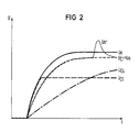
- the operating voltage (input voltage Ue) present at the input of the voltage regulator 1 has the profile shown in FIG. 2, namely after the switch-on process it reaches the end value within a certain time after an approximately e-function profile.
- the capacitors C1 in the output-side transverse branch of the voltage regulator 1 and C3 in the source circuit of the transistor Tr are charged to the output voltage Ua.
- the capacitor C1 as a memory at the output of the voltage regulator 1 is provided in order to avoid a reduction in the amplitude of the desired voltage peak by the voltage regulator.
- the voltage Ua at the output of the voltage regulator upstream of the choke, which corresponds to the voltage at the capacitor C1 is lower than the input voltage Ue, as can be seen in FIG. 2.
- This superposition of the two voltages occurs when, after the same input voltages have been reached at the inputs X and Y of the comparator 2, ie if the voltages U C4 and U D1 are the same, the comparator 2 controls the transistor Tr in such a way that it is switched to the open position.
- the transistor can of course also be replaced by a corresponding element with a switch function, for example a relay.
- the breakdown voltage of the Zener diode D1 is selected so that it is less than the input voltage Ue and greater than the voltage which leads to the vibration breaking off when the Gunn supply voltage is reduced.
- a time must be set until the switching threshold of the comparator is reached, which is greater than the charging time of the capacitors C3 and C1. So that will ensures that the capacitors C3 and C1 are already charged before the comparator output turns on the transistor and the voltage U C3 of the capacitor C3 is superimposed on the output voltage Ua on the capacitor C1.
- the amplitude of the voltage peak can be set by varying the capacitance values of the capacitors C1, C2 and C3.
- the diode D3 between the connection point of the voltage divider R1 / C4 and the circuit input is used to quickly discharge the capacitor C4 when the supply voltage Ue drops. This ensures that a defined switch-on time for the supply voltage is reached again.
- the circuit described above is implemented with a voltage regulator, the regulator being an expression for a stable voltage of a voltage source. What is essential, however, is only the fact that a stable voltage is briefly applied a second voltage via a corresponding time element.
Landscapes
- Engineering & Computer Science (AREA)
- Physics & Mathematics (AREA)
- Electromagnetism (AREA)
- General Physics & Mathematics (AREA)
- Radar, Positioning & Navigation (AREA)
- Automation & Control Theory (AREA)
- Dc-Dc Converters (AREA)
Claims (5)
- Régulateur de tension servant à accroître pendant un bref intervalle de temps une tension d'alimentation réglée d'un oscillateur Gunn lors du branchement et dans le cas d'une chute de tension, caractérisé en ce que du côté entrée, et en parallèle avec le régulateur de tension (1), est branché un circuit de temporisation (2) dont le signal de sortie est envoyé à un élément de commutation (Tr), et qu'en outre il est prévu un condensateur (C3) entre l'élément de commutation (Tr) et la sortie du régulateur de tension (C1) pour l'obtention de l'accroissement de tension désiré, la tension aux bornes du condensateur étant superposée, en tant que pointe de tension décalée d'un intervalle de temps réglable, à la sortie de tension du régulateur de tension (1), par l'intermédiaire de l'élément de commutation (Tr).
- Régulateur de tension suivant la revendication 1, caractérisé par le fait que le circuit de temporisation (2) est constitué par un comparateur à deux entrées, à une entrée duquel est appliquée la tension partielle d'un diviseur de tension constitué par une résistance (R4) et une capacité (C4), et à l'autre entrée duquel est appliquée une tension qui est réglable au moyen d'une diode Zener (D1), et dont le signal de sortie, qui est formé en cas d'égalité des tensions, place l'élément de commutation (Tr) à l'état conducteur.
- Régulateur de tension suivant la revendication 1 ou 2, caractérisé par le fait que la constante de temps du circuit de temporisation (2) est dimensionnée de manière que l'intervalle de temps s'étendant jusqu'à ce que le seuil de commutation soit atteint est supérieur au temps de charge du condensateur (C3) situé entre l'élément de commutation (Tr) et la sortie du régulateur de tension (1) ainsi que d'un autre condensateur (C1) branché à la sortie du régulateur de tension.
- Régulateur de tension suivant l'une des revendications 1 à 3, caractérisé par le fait que l'élément de commutation (Tr) est constitué par un transistor.
- Régulateur de tension suivant l'une des revendications 1 à 4, caractérisé par le fait qu'une diode (D3) est branchée entre les points de liaision du diviseur de tension et la borne de raccordement de la tension de service.
Applications Claiming Priority (2)
| Application Number | Priority Date | Filing Date | Title |
|---|---|---|---|
| DE3733071 | 1987-09-30 | ||
| DE3733071 | 1987-09-30 |
Publications (3)
| Publication Number | Publication Date |
|---|---|
| EP0309922A2 EP0309922A2 (fr) | 1989-04-05 |
| EP0309922A3 EP0309922A3 (en) | 1989-08-02 |
| EP0309922B1 true EP0309922B1 (fr) | 1992-12-23 |
Family
ID=6337314
Family Applications (1)
| Application Number | Title | Priority Date | Filing Date |
|---|---|---|---|
| EP88115591A Expired - Lifetime EP0309922B1 (fr) | 1987-09-30 | 1988-09-22 | Circuit pour élever temporairement une tension régulée, au moment de la mise sous tension et en cas de chute de tension |
Country Status (2)
| Country | Link |
|---|---|
| EP (1) | EP0309922B1 (fr) |
| DE (1) | DE3876923D1 (fr) |
Families Citing this family (1)
| Publication number | Priority date | Publication date | Assignee | Title |
|---|---|---|---|---|
| FR2798480B1 (fr) * | 1999-09-10 | 2001-10-26 | St Microelectronics Sa | Regulateur de tension |
Family Cites Families (1)
| Publication number | Priority date | Publication date | Assignee | Title |
|---|---|---|---|---|
| US3697856A (en) * | 1970-12-14 | 1972-10-10 | Us Navy | Voltage regulating circuit |
-
1988
- 1988-09-22 DE DE8888115591T patent/DE3876923D1/de not_active Expired - Fee Related
- 1988-09-22 EP EP88115591A patent/EP0309922B1/fr not_active Expired - Lifetime
Also Published As
| Publication number | Publication date |
|---|---|
| DE3876923D1 (de) | 1993-02-04 |
| EP0309922A2 (fr) | 1989-04-05 |
| EP0309922A3 (en) | 1989-08-02 |
Similar Documents
| Publication | Publication Date | Title |
|---|---|---|
| DE69102592T2 (de) | Spannungsgesteuerte ausgeglichene Quarzoszillatorschaltung. | |
| EP0404230A2 (fr) | Boucle à verrouillage de phase | |
| DE3318536A1 (de) | Durchstimmbare schaltungsanordnung | |
| DE69500119T2 (de) | Anordnung zum Steuern einer Niederdruckleuchtstofflampe | |
| DE2539632A1 (de) | Kristalloszillator | |
| DE1959162A1 (de) | Digital arbeitender Frequenzgenerator | |
| EP0309922B1 (fr) | Circuit pour élever temporairement une tension régulée, au moment de la mise sous tension et en cas de chute de tension | |
| EP1586183A1 (fr) | Ensemble oscillateur utilise a des fins de modulation de frequence | |
| DE4232026C2 (de) | Elektrostatische Beschichtungspistole und Verfahren zum Erzeugen einer Hochspannung | |
| DE2811080A1 (de) | Durch spannungsaenderung abstimmbarer hochfrequenz-oszillator | |
| DE3751078T2 (de) | Quartz-Oszillator mit breitem Ziehbereich. | |
| DE2557134A1 (de) | Transistoroszillator | |
| DE2001660A1 (de) | Abstimmschaltung fuer eine Vielzahl elektronisch abstimmbarer Schaltkreise | |
| DE3931513A1 (de) | Phasenregelschleife fuer die direktmodulation | |
| EP1526623B1 (fr) | Circuit de limitation d'un courant d'appel | |
| DE3124492C2 (fr) | ||
| DE3914287A1 (de) | Gleichspannungswandler | |
| DE1766840C (de) | Amplitudengeregelter Generator | |
| DE19535695C2 (de) | Spannungsgesteuerter Oszillator | |
| DE2701353A1 (de) | Mischstufe mit kapazitiver einkopplung der oszillatorfrequenz | |
| EP0759657A1 (fr) | Procédé pour accorder un circuit résonnant par changement de la tension d'alimentation d'une diode à capacité variable | |
| DE3930751A1 (de) | Schaltungsanordnung zur taktrueckgewinnung | |
| EP1515443B1 (fr) | Stabilisation de fréquence d'un oscillateur commandé en courant appliqué comme horloge basse fréquence dans un radiotéléphone mobile | |
| DE2929897A1 (de) | Spannungsgesteuerter oszillator | |
| DE3730773A1 (de) | Hochfrequenz-generator |
Legal Events
| Date | Code | Title | Description |
|---|---|---|---|
| PUAI | Public reference made under article 153(3) epc to a published international application that has entered the european phase |
Free format text: ORIGINAL CODE: 0009012 |
|
| AK | Designated contracting states |
Kind code of ref document: A2 Designated state(s): CH DE FR GB IT LI NL |
|
| PUAL | Search report despatched |
Free format text: ORIGINAL CODE: 0009013 |
|
| AK | Designated contracting states |
Kind code of ref document: A3 Designated state(s): CH DE FR GB IT LI NL |
|
| 17P | Request for examination filed |
Effective date: 19891206 |
|
| 17Q | First examination report despatched |
Effective date: 19920430 |
|
| GRAA | (expected) grant |
Free format text: ORIGINAL CODE: 0009210 |
|
| AK | Designated contracting states |
Kind code of ref document: B1 Designated state(s): CH DE FR GB IT LI NL |
|
| PG25 | Lapsed in a contracting state [announced via postgrant information from national office to epo] |
Ref country code: FR Free format text: THE PATENT HAS BEEN ANNULLED BY A DECISION OF A NATIONAL AUTHORITY Effective date: 19921223 |
|
| REF | Corresponds to: |
Ref document number: 3876923 Country of ref document: DE Date of ref document: 19930204 |
|
| ET | Fr: translation filed | ||
| ITF | It: translation for a ep patent filed | ||
| GBT | Gb: translation of ep patent filed (gb section 77(6)(a)/1977) |
Effective date: 19930301 |
|
| PG25 | Lapsed in a contracting state [announced via postgrant information from national office to epo] |
Ref country code: GB Effective date: 19930922 |
|
| PG25 | Lapsed in a contracting state [announced via postgrant information from national office to epo] |
Ref country code: LI Effective date: 19930930 Ref country code: CH Effective date: 19930930 |
|
| PLBE | No opposition filed within time limit |
Free format text: ORIGINAL CODE: 0009261 |
|
| STAA | Information on the status of an ep patent application or granted ep patent |
Free format text: STATUS: NO OPPOSITION FILED WITHIN TIME LIMIT |
|
| 26N | No opposition filed | ||
| PG25 | Lapsed in a contracting state [announced via postgrant information from national office to epo] |
Ref country code: NL Effective date: 19940401 |
|
| NLV4 | Nl: lapsed or anulled due to non-payment of the annual fee | ||
| GBPC | Gb: european patent ceased through non-payment of renewal fee |
Effective date: 19930922 |
|
| REG | Reference to a national code |
Ref country code: CH Ref legal event code: PL |
|
| PG25 | Lapsed in a contracting state [announced via postgrant information from national office to epo] |
Ref country code: DE Effective date: 19940601 |
|
| REG | Reference to a national code |
Ref country code: FR Ref legal event code: ST |
|
| PG25 | Lapsed in a contracting state [announced via postgrant information from national office to epo] |
Ref country code: IT Free format text: LAPSE BECAUSE OF NON-PAYMENT OF DUE FEES;WARNING: LAPSES OF ITALIAN PATENTS WITH EFFECTIVE DATE BEFORE 2007 MAY HAVE OCCURRED AT ANY TIME BEFORE 2007. THE CORRECT EFFECTIVE DATE MAY BE DIFFERENT FROM THE ONE RECORDED. Effective date: 20050922 |