EP0309769B1 - Spannungsgesteuerter Oszillator mit einem keramischen Schwingquarz - Google Patents
Spannungsgesteuerter Oszillator mit einem keramischen Schwingquarz Download PDFInfo
- Publication number
- EP0309769B1 EP0309769B1 EP88114401A EP88114401A EP0309769B1 EP 0309769 B1 EP0309769 B1 EP 0309769B1 EP 88114401 A EP88114401 A EP 88114401A EP 88114401 A EP88114401 A EP 88114401A EP 0309769 B1 EP0309769 B1 EP 0309769B1
- Authority
- EP
- European Patent Office
- Prior art keywords
- input
- output
- amplifier
- voltage
- controllable
- Prior art date
- Legal status (The legal status is an assumption and is not a legal conclusion. Google has not performed a legal analysis and makes no representation as to the accuracy of the status listed.)
- Expired - Lifetime
Links
- 239000000919 ceramic Substances 0.000 title claims abstract description 19
- 239000013078 crystal Substances 0.000 title claims description 17
- 239000010453 quartz Substances 0.000 description 13
- VYPSYNLAJGMNEJ-UHFFFAOYSA-N silicon dioxide Inorganic materials O=[Si]=O VYPSYNLAJGMNEJ-UHFFFAOYSA-N 0.000 description 13
- 230000010363 phase shift Effects 0.000 description 4
Images
Classifications
-
- H—ELECTRICITY
- H03—ELECTRONIC CIRCUITRY
- H03B—GENERATION OF OSCILLATIONS, DIRECTLY OR BY FREQUENCY-CHANGING, BY CIRCUITS EMPLOYING ACTIVE ELEMENTS WHICH OPERATE IN A NON-SWITCHING MANNER; GENERATION OF NOISE BY SUCH CIRCUITS
- H03B5/00—Generation of oscillations using amplifier with regenerative feedback from output to input
- H03B5/30—Generation of oscillations using amplifier with regenerative feedback from output to input with frequency-determining element being electromechanical resonator
- H03B5/32—Generation of oscillations using amplifier with regenerative feedback from output to input with frequency-determining element being electromechanical resonator being a piezoelectric resonator
- H03B5/36—Generation of oscillations using amplifier with regenerative feedback from output to input with frequency-determining element being electromechanical resonator being a piezoelectric resonator active element in amplifier being semiconductor device
-
- H—ELECTRICITY
- H03—ELECTRONIC CIRCUITRY
- H03B—GENERATION OF OSCILLATIONS, DIRECTLY OR BY FREQUENCY-CHANGING, BY CIRCUITS EMPLOYING ACTIVE ELEMENTS WHICH OPERATE IN A NON-SWITCHING MANNER; GENERATION OF NOISE BY SUCH CIRCUITS
- H03B2200/00—Indexing scheme relating to details of oscillators covered by H03B
- H03B2200/0014—Structural aspects of oscillators
- H03B2200/002—Structural aspects of oscillators making use of ceramic material
-
- H—ELECTRICITY
- H03—ELECTRONIC CIRCUITRY
- H03B—GENERATION OF OSCILLATIONS, DIRECTLY OR BY FREQUENCY-CHANGING, BY CIRCUITS EMPLOYING ACTIVE ELEMENTS WHICH OPERATE IN A NON-SWITCHING MANNER; GENERATION OF NOISE BY SUCH CIRCUITS
- H03B2200/00—Indexing scheme relating to details of oscillators covered by H03B
- H03B2200/0014—Structural aspects of oscillators
- H03B2200/0026—Structural aspects of oscillators relating to the pins of integrated circuits
Definitions
- the invention relates to a voltage-controlled oscillator with a ceramic quartz crystal.
- a quartz oscillator circuit with phase shifters in the feedback circuit is known, in which the phase position is determined by adding two signals of different phase positions, the relationship of which to one another can be changed.
- the output of the oscillator is connected to the input of a first phase shifter.
- the output of the first phase shifter is connected to the first input of a summation circuit via a first feedback branch, in which a second phase shifter and an amplifier are located.
- the output of the first phase shifter is also connected via a second feedback branch, in which a multiplier is located, to the second input of the summation circuit, the output of which is connected to the input of the oscillator.
- DE-OS 21 31 159 also describes an oscillator circuit with phase shifters in the feedback circuit, in which the phase position is determined by adding two signals of different phase positions, the relationship of which to one another can be changed.
- the output of the oscillator is connected to the input of an amplifier.
- the output of the amplifier is connected to a summation circuit, the output of which is fed back to the oscillator, via a parallel circuit comprising a first phase shifter for phase advance and a second phase shifter for phase delay.
- Integrated circuits in which voltage-controlled oscillators are integrated, have several connections, so-called pins.
- the developer When designing an integrated circuit, the developer always strives to design the circuits so that as few pins as possible are required.
- the invention solves this problem in that the output voltage of the ceramic quartz crystal the input of a phase shifter with two parallel connected branches is fed that in one branch there is an amplifier, in the other branch there is a low pass, a controllable amplifier and a controllable changeover switch, the first input of which is connected to the output of the controllable amplifier, the second input of which is at reference potential and whose Output is connected to the first input of a summer, that the output of the amplifier is connected to the second input of the summer and that the output of the summer is fed back to the ceramic quartz crystal.
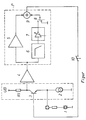
- one connection of a parallel circuit consisting of a ceramic quartz crystal 1 and a current source 2 is at reference potential, while the other connection is connected to the emitter of a transistor 3.
- the collector of transistor 3 is connected to the input of an amplifier 4 and is connected to a supply voltage UB via a resistor 3.
- the output of the amplifier 4 is connected to the input of an amplifier 5 and a low pass 6, the output of which is connected to the input of a controllable amplifier 7.
- the output of the controllable amplifier 7 is connected to the first input of a controllable switch 8, the second input of which is at reference potential.
- the output of the controllable switch 8 is connected to the first input of a summer 9, the second input of which is connected to the output of the amplifier 5.
- the output of the summer 9 can be fed back to the base of the transistor 3 via a controllable switch 10.
- the amplifier 5 is in one branch, the low-pass filter 6, the controllable amplifier 7 and the controllable switch 8 are in the other branch of the phase shifter P. If the phase shift between the signal at the first and at the second input of the summer 9 is zero, the oscillates ceramic quartz crystal with its resonance frequency. This case is realized by setting the gain of the control amplifier 7 to zero. However, this state can be achieved more precisely and simply by the controllable changeover switch 8 being in its position second input is switched so that the first input of the summer 9 is at reference potential. If the voltage-controlled oscillator is to change its frequency, the controllable switch 8 is to be switched over so that its first input is connected to the output.
- the gain of the controllable amplifier 7 is now chosen to be positive, the result is a phase shift which is greater than zero.
- a phase shift that is greater than zero for example, the frequency of the ceramic quartz crystal is increased, while it is reduced with a phase shift that is less than zero.
- a reduction in the frequency of the ceramic quartz crystal is therefore achieved in that the gain of the controllable amplifier 7 is chosen negatively.
- the voltage-controlled oscillator By changing the voltage at the control input of the controllable amplifier 7, the frequency of the ceramic quartz crystal 1 and thus of the voltage-controlled oscillator is changed in the embodiment shown in the figure.
- the controllable switch 8 By switching the controllable switch 8, the voltage-controlled oscillator can be set immediately and precisely to the resonance frequency of the ceramic quartz crystal.
Landscapes
- Oscillators With Electromechanical Resonators (AREA)
- Stabilization Of Oscillater, Synchronisation, Frequency Synthesizers (AREA)
- Organic Low-Molecular-Weight Compounds And Preparation Thereof (AREA)
- Photoreceptors In Electrophotography (AREA)
- Developing Agents For Electrophotography (AREA)
- Inductance-Capacitance Distribution Constants And Capacitance-Resistance Oscillators (AREA)
Description
- Die Erfindung betrifft einen spannungsgesteuerten Oszillator mit einem keramischen Schwingquarz.
- Es sind Fernsehgeräte mit einem Teletextdecoder bekannt, bei denen einige Seiten Teletext speicherbar sind und auf dem Bildschirm angezeigt werden können. Um ein Flimmern des Bildes mit Sicherheit zu vermeiden, ist ein sehr genauer spannungsgesteuerter Oszillator nötig. Meist wird ein spannungsgesteuerter Oszillator mit einem keramischen Schwingquarz verwendet.
- Aus der GB-A 2 053 608 ist eine Quarzoszillatorschaltung mit Phasenschiebern im Rückkopplungskreis bekannt, bei denen die Phasenlage durch Addition zweier Signale unterschiedlicher Phasenlage, deren Verhältnis zueinander verändert werden kann, bestimmt wird.
- Bei dieser Oszillatorschaltung ist der Ausgang des Oszillators mit dem Eingang eines ersten Phasenschiebers verbunden. Der Ausgang des ersten Phasenschiebers ist über einen ersten Rückkopplungszweig, in dem ein zweiter Phasenschieber und ein Verstärker liegen, mit dem ersten Eingang einer Summationsschaltung verbunden. Der Ausgang des ersten Phasenschiebers ist außerdem über einen zweiten Rückkopplungszweig, in dem ein Multiplizierer liegt, mit dem zweiten Eingang der Summationsschaltung verbunden, deren Ausgang mit dem Eingang des Oszillators verbunden ist.
- In der DE-OS 21 31 159 ist ebenfalls eine Oszillatorschaltung mit Phasenschiebern im Rückkopplungskreis beschrieben, bei denen die Phasenlage durch Addition zweier Signale unterschiedlicher Phasenlage, deren Verhältnis zueinander verändert werden kann, bestimmt wird.
- In dieser Oszillatorschaltung ist der Ausgang des Oszillators mit dem Eingang eines Verstärkers verbunden. Der Ausgang des Verstärkers ist über eine Parallelschaltung aus einem ersten Phasenschieber zur Phasenvorauseilung und einem zweiten Phasenschieber zur Phasenverzögerung mit einer Summationsschaltung verbunden, deren Ausgang auf der Oszillator rückgekoppelt ist.
- Integrierte Schaltkreise, in denen spannungsgesteuerte Oszillatoren integriert sind, weisen mehrere Anschlüsse, sogenannte Pins, auf. Beim Entwurf eines integrierten Schaltkreises trachtet der Entwickler stets danach, die Schaltkreise so zu entwerfen, daß möglichst wenige Pins erforderlich sind.
- Es ist daher Aufgabe der Erfindung, einen spannungsgesteuerten Oszillator mit einem keramischen Schwingquarz so zu gestalten, daß er mit nur einem Pin zum Anschluß des keramischen Schwingquarzes auskommt, und trotzdem seine Frequenz mittels einer Spannung steuerbar ist.
- Die Erfindung löst diese Aufgabe dadurch, daß die Ausgangsspannung des keramischen Schwingquarzes dem Eingang eines Phasenschiebers mit zwei parallel geschalteten Zweigen zugeführt wird, daß in einem Zweig ein Verstärker liegt, daß im anderen Zweig ein Tiefpaß, ein regelbarer Verstärker und ein steuerbarer Umschalter liegen, dessen erster Eingang mit dem Ausgang des regelbaren Verstärkers verbunden ist, dessen zweiter Eingang auf Bezugspotential liegt und dessen Ausgang mit dem ersten Eingang eines Summierers verbunden ist, daß der Ausgang des Verstärkers mit dem zweiten Eingang des Summierers verbunden ist und daß der Ausgang des Summierers auf den keramischen Schwingquarz rückgekoppelt ist.
- Anhand des in der Figur gezeigten Ausführungsbeispieles wird die Erfindung zuerst beschrieben und anschließend erläutert.
- In der Figur 1 liegt der eine Anschluß einer Parallelschaltung aus einem keramischen Schwingquarz 1 und einer Stromquelle 2 auf Bezugspotential, während der andere Anschluß mit dem Emitter eines Transistors 3 verbunden ist. Der Kollektor des Transistors 3 ist mit dem Eingang eines Verstärkers 4 verbunden und liegt über einen Widerstand 3 an einer Versorgungsspannung UB. Der Ausgang des Verstärkers 4 ist mit dem Eingang eines Verstärkers 5 und eines Tiefpasses 6 verbunden, dessen Ausgang mit dem Eingang eines regelbaren Verstärkers 7 verbunden ist. Der Ausgang des regelbaren Verstärkers 7 ist mit dem ersten Eingang eines steuerbaren Umschalters 8 verbunden, dessen zweiter Eingang auf Bezugspotential liegt. Der Ausgang des steuerbaren Umschalters 8 ist mit dem ersten Eingang eines Summierers 9 verbunden, dessen zweiter Eingang mit dem Ausgang des Verstärkers 5 verbunden ist. Der Ausgang des Summierers 9 ist über einen steuerbaren Schalter 10 auf die Basis des Transistors 3 rückkoppelbar.
- Der Verstärker 5 liegt im einen Zweig, der Tiefpaß 6, der regelbare Verstärker 7 und der steuerbare Umschalter 8 liegen im anderen Zweig des Phasenschiebers P. Wenn die Phasenverschiebung zwischen dem Signal am ersten und am zweiten Eingang des Summierers 9 null beträgt, so schwingt der keramische Schwingquarz mit seiner Resonanzfrequenz. Dieser Fall wird realisiert, indem die Verstärkung des Regelverstärkers 7 auf null gestellt wird. Genauer und einfacher läßt sich dieser Zustand aber dadurch erzielen, daß der steuerbare Umschalter 8 auf seinen zweiten Eingang umgeschaltet wird, so daß der erste Eingang des Summierers 9 auf Bezugspotential liegt. Soll nun der spannungsgesteuerte Oszillator seine Frequenz ändern, so ist der steuerbare Schalter 8 umzuschalten, so daß sein erster Eingang mit dem Ausgang verbunden ist. Wird nun die Verstärkung des regelbaren Verstärkers 7 positiv gewählt, so ergibt sich eine Phasenverschiebung, die größer als null ist. Bei einer Phasenverschiebung, die größer als null ist, wird beispielsweise die Frequenz des keramischen Schwingquarzes erhöht, während sie bei einer Phasenverschiebung die kleiner als null ist, erniedrigt wird. Eine Verringerung der Frequenz des keramischen Schwingquarzes wird deshalb dadurch erzielt, daß die Verstärkung des regelbaren Verstärkers 7 negativ gewählt wird.
- Durch Verändern der Spannung am Regeleingang des regelbaren Verstärkers 7 wird bei dem in der Figur gezeigten Ausführungsbeispiel die Frequenz des keramischen Schwingquarzes 1 und damit des spannungsgesteuerten Oszillators verändert. Durch Umschalten des steuerbaren Umschalters 8 kann der spannungsgesteuerte Oszillator sofort und genau auf die Resonanzfrequenz des keramischen Schwingquarzes eingestellt werden.
Claims (2)
- Spannungsgesteuerter Oszillator mit einem keramischen Schwingquarz (1), dadurch gekennzeichnet, daß die Ausgangsspannung des keramischen Schwingquarzes (1) dem Eingang eines Phasenschiebers (P) mit zwei parallel geschalteten Zweigen zugeführt wird, daß im einen Zweig ein Verstärker (5) liegt, daß im anderen Zweig ein Tiefpaß (6), ein regelbarer Verstärker (7) und ein steuerbarer Umschalter (8) liegen, dessen erster Eingang mit dem Ausgang des regelbaren Verstärkers (7) verbunden ist, dessen zweiter Eingang auf Bezugspotential liegt und dessen Ausgang mit dem ersten Eingang eines Summierers (9) verbunden ist, daß der Ausgang des Verstärkers (5) mit dem zweiten Eingang des Summierers (9) verbunden ist und daß der Ausgang des Summierers (9) auf den keramischen Schwingquarz (1) rückgekoppelt ist.
- Spannungsgesteuerter Oszillator nach Anspruch 1, dadurch gekennzeichnet, daß der eine Anschluß einer Parallelschaltung aus dem keramischen Schwingquarz (1) und einer Stromquelle (2) auf Bezugspotential liegt, während ihre anderer Anschluß mit dem Emitter eines Transistors (3) verbunden ist, daß der Kollektor des Transistors (3) mit dem Eingang eines ersten Verstärkers (4) verbunden ist und über einen Widerstand (R1) an einer Versorgungsspannung (UB) liegt, daß der Ausgang des ersten Verstärkers (4) mit dem Eingang eines zweiten Verstärkers (5) und eines Tiefpasses (6) verbunden ist, daß der Ausgang des Tiefpasses (6) mit dem Eingang eines regelbaren Verstärkers (7) verbunden ist, dessen Ausgang mit dem ersten Eingang eines steuerbaren Umschalters (8) verbunden ist, daß der zweite Eingang des steuerbaren Umschalters (8) auf Bezugspotential liegt, daß der Ausgang des steuerbaren Umschalters (8) mit dem ersten Eingang eines Summierers (9) verbunden ist, dessen zweiter Eingang mit dem Ausgang des zweiten Verstärkers (5) verbunden ist und dessen Ausgang über einen steuerbaren Schalter (10) mit der Basis des Transistors (3) verbunden ist.
Priority Applications (1)
| Application Number | Priority Date | Filing Date | Title |
|---|---|---|---|
| AT88114401T ATE87153T1 (de) | 1987-09-30 | 1988-09-03 | Spannungsgesteuerter oszillator mit einem keramischen schwingquarz. |
Applications Claiming Priority (2)
| Application Number | Priority Date | Filing Date | Title |
|---|---|---|---|
| DE19873732906 DE3732906A1 (de) | 1987-09-30 | 1987-09-30 | Spannungsgesteuerter oszillator mit einem keramischen schwingquarz |
| DE3732906 | 1987-09-30 |
Publications (2)
| Publication Number | Publication Date |
|---|---|
| EP0309769A1 EP0309769A1 (de) | 1989-04-05 |
| EP0309769B1 true EP0309769B1 (de) | 1993-03-17 |
Family
ID=6337193
Family Applications (1)
| Application Number | Title | Priority Date | Filing Date |
|---|---|---|---|
| EP88114401A Expired - Lifetime EP0309769B1 (de) | 1987-09-30 | 1988-09-03 | Spannungsgesteuerter Oszillator mit einem keramischen Schwingquarz |
Country Status (8)
| Country | Link |
|---|---|
| US (1) | US4888567A (de) |
| EP (1) | EP0309769B1 (de) |
| JP (1) | JP2735582B2 (de) |
| KR (1) | KR960009964B1 (de) |
| AT (1) | ATE87153T1 (de) |
| DE (2) | DE3732906A1 (de) |
| ES (1) | ES2039535T3 (de) |
| FI (1) | FI884439A7 (de) |
Families Citing this family (4)
| Publication number | Priority date | Publication date | Assignee | Title |
|---|---|---|---|---|
| DE4310552C2 (de) * | 1993-03-31 | 1995-05-04 | Siemens Ag | Colpitts-Oszillator |
| US5731744A (en) * | 1996-05-28 | 1998-03-24 | Brooktree Corporation | Voltage controlled oscillator |
| JPH11330876A (ja) | 1998-05-15 | 1999-11-30 | Nec Corp | 電圧制御増幅回路 |
| DE102013209364A1 (de) * | 2013-05-21 | 2014-11-27 | Friedrich-Alexander-Universität Erlangen-Nürnberg | Verfahren zur Messung der Frequenz eines elektrischen Signals sowie elektrisches Messsystem |
Family Cites Families (4)
| Publication number | Priority date | Publication date | Assignee | Title |
|---|---|---|---|---|
| US3691475A (en) * | 1970-07-24 | 1972-09-12 | Hitachi Ltd | Voltage controlled oscillator |
| FR2506100A2 (fr) * | 1975-06-06 | 1982-11-19 | Telediffusion Fse | Systeme de diffusion de donnees |
| US4286235A (en) * | 1979-06-25 | 1981-08-25 | Rca Corporation | VFO having plural feedback loops |
| US4733200A (en) * | 1986-10-14 | 1988-03-22 | Motorola, Inc. | Controlled feedback path voltage controlled oscillator |
-
1987
- 1987-09-30 DE DE19873732906 patent/DE3732906A1/de not_active Withdrawn
-
1988
- 1988-09-03 EP EP88114401A patent/EP0309769B1/de not_active Expired - Lifetime
- 1988-09-03 DE DE8888114401T patent/DE3879343D1/de not_active Expired - Fee Related
- 1988-09-03 ES ES198888114401T patent/ES2039535T3/es not_active Expired - Lifetime
- 1988-09-03 AT AT88114401T patent/ATE87153T1/de not_active IP Right Cessation
- 1988-09-27 KR KR1019880012457A patent/KR960009964B1/ko not_active Expired - Fee Related
- 1988-09-28 JP JP63241200A patent/JP2735582B2/ja not_active Expired - Fee Related
- 1988-09-28 FI FI884439A patent/FI884439A7/fi not_active Application Discontinuation
- 1988-09-28 US US07/250,731 patent/US4888567A/en not_active Expired - Lifetime
Also Published As
| Publication number | Publication date |
|---|---|
| JPH01144806A (ja) | 1989-06-07 |
| ATE87153T1 (de) | 1993-04-15 |
| KR960009964B1 (ko) | 1996-07-25 |
| US4888567A (en) | 1989-12-19 |
| JP2735582B2 (ja) | 1998-04-02 |
| FI884439A7 (fi) | 1989-03-31 |
| DE3732906A1 (de) | 1989-04-13 |
| ES2039535T3 (es) | 1993-10-01 |
| FI884439A0 (fi) | 1988-09-28 |
| EP0309769A1 (de) | 1989-04-05 |
| KR890005968A (ko) | 1989-05-18 |
| DE3879343D1 (de) | 1993-04-22 |
Similar Documents
| Publication | Publication Date | Title |
|---|---|---|
| DE4018614C2 (de) | Schaltungsanordnung zur Erzeugung zweier phasenverschobener Ausgangssignale | |
| DE3829164C1 (de) | ||
| EP1189337B1 (de) | Gegentaktmischerschaltung unter Verwendung von bipolaren Transistoren | |
| EP0309769B1 (de) | Spannungsgesteuerter Oszillator mit einem keramischen Schwingquarz | |
| DE10126236B4 (de) | Verstärker | |
| EP0254072B1 (de) | Schaltungsanordnung zum Verschieben der Phase eines Signals | |
| DE3544342C1 (de) | Regelschaltung zum Abgleich einer Laufzeitleitung | |
| DE1156844B (de) | Saegezahnspannungsgenerator, insbesondere zur zeitlinearen Ablenkung des Abtastflecks von Elektronenstrahlen | |
| DE2649745C2 (de) | Frequenzsteuerbarer Oszillator | |
| EP0426900B1 (de) | Integrierbare frequenzvariable Oszillatorschaltung | |
| DE10217852B4 (de) | Verfahren und Vorrichtung zur Ansteuerung eines Oszillators oder einer Phasenverzögerungseinrichtung in einem Phasenregelkreis | |
| EP0093899B1 (de) | Anordnung zur Anpassung einer Prüfeinrichtung an einen Prüfling | |
| DE69909086T2 (de) | Schaltung und deren Verwendung zur Reduzierung von Verzerrungen und Störungen von Rechteckimpulsen | |
| DE102007019745A1 (de) | Kaskadierter Phasenschieber | |
| EP0448835A1 (de) | Phasenteiler | |
| DE1924680B2 (de) | Transistor-mischschaltung | |
| DE69303092T2 (de) | Elektrischer Schaltkreis mit Ortsoszillatorkreis und Ortsoszillator für einen solchen Schaltkreis | |
| DE3901298C2 (de) | ||
| DE3327427A1 (de) | Generator fuer rechteckspannungen variabler phase | |
| EP0744832B1 (de) | Schaltungsanordnung zum Erzeugen eines gegenüber einem Eingangssignal orthogonalen Ausgangssignal sowie Verwendungen dieser Schaltungsanordnung | |
| DE2810604C3 (de) | Verfahren und Schaltungsanordnung zur Erzeugung zweier Farbträgersignale mit konjugiert-komplexer Phasenlage | |
| DE3924502C1 (en) | XOR coupling circuitry for two signals - has two pre=emphasis stages between input stages and two current-switching groups | |
| DE4121736C1 (en) | Switching pulses generating circuitry e.g. for vertical deflection in TV receiver - has oscillator with capacitor controlled from current sources and connected via terminal to integrated circuit | |
| DE3244674C2 (de) | Schaltung für die Erzeugung von gegenseitig um 90° phasenverschobenen Hochfrequenzsignalen | |
| EP0082380A1 (de) | Elektronischer Verstärker mit einem durch eine Steuerspannung veränderbaren Übertragungsmass, insbesondere Expander |
Legal Events
| Date | Code | Title | Description |
|---|---|---|---|
| PUAI | Public reference made under article 153(3) epc to a published international application that has entered the european phase |
Free format text: ORIGINAL CODE: 0009012 |
|
| AK | Designated contracting states |
Kind code of ref document: A1 Designated state(s): AT BE CH DE ES FR GB GR IT LI LU NL SE |
|
| 17P | Request for examination filed |
Effective date: 19890930 |
|
| 17Q | First examination report despatched |
Effective date: 19910925 |
|
| GRAA | (expected) grant |
Free format text: ORIGINAL CODE: 0009210 |
|
| AK | Designated contracting states |
Kind code of ref document: B1 Designated state(s): AT BE CH DE ES FR GB GR IT LI LU NL SE |
|
| REF | Corresponds to: |
Ref document number: 87153 Country of ref document: AT Date of ref document: 19930415 Kind code of ref document: T |
|
| ITF | It: translation for a ep patent filed | ||
| REF | Corresponds to: |
Ref document number: 3879343 Country of ref document: DE Date of ref document: 19930422 |
|
| GBT | Gb: translation of ep patent filed (gb section 77(6)(a)/1977) |
Effective date: 19930420 |
|
| ET | Fr: translation filed | ||
| REG | Reference to a national code |
Ref country code: GR Ref legal event code: FG4A Free format text: 3008163 |
|
| REG | Reference to a national code |
Ref country code: ES Ref legal event code: FG2A Ref document number: 2039535 Country of ref document: ES Kind code of ref document: T3 |
|
| EPTA | Lu: last paid annual fee | ||
| PLBE | No opposition filed within time limit |
Free format text: ORIGINAL CODE: 0009261 |
|
| STAA | Information on the status of an ep patent application or granted ep patent |
Free format text: STATUS: NO OPPOSITION FILED WITHIN TIME LIMIT |
|
| 26N | No opposition filed | ||
| EAL | Se: european patent in force in sweden |
Ref document number: 88114401.8 |
|
| PGFP | Annual fee paid to national office [announced via postgrant information from national office to epo] |
Ref country code: AT Payment date: 19990923 Year of fee payment: 12 |
|
| PGFP | Annual fee paid to national office [announced via postgrant information from national office to epo] |
Ref country code: SE Payment date: 19990924 Year of fee payment: 12 |
|
| PGFP | Annual fee paid to national office [announced via postgrant information from national office to epo] |
Ref country code: LU Payment date: 19990927 Year of fee payment: 12 Ref country code: GR Payment date: 19990927 Year of fee payment: 12 Ref country code: CH Payment date: 19990927 Year of fee payment: 12 Ref country code: BE Payment date: 19990927 Year of fee payment: 12 |
|
| PGFP | Annual fee paid to national office [announced via postgrant information from national office to epo] |
Ref country code: NL Payment date: 19990930 Year of fee payment: 12 |
|
| PG25 | Lapsed in a contracting state [announced via postgrant information from national office to epo] |
Ref country code: LU Free format text: LAPSE BECAUSE OF NON-PAYMENT OF DUE FEES Effective date: 20000903 Ref country code: AT Free format text: LAPSE BECAUSE OF NON-PAYMENT OF DUE FEES Effective date: 20000903 |
|
| PG25 | Lapsed in a contracting state [announced via postgrant information from national office to epo] |
Ref country code: SE Free format text: THE PATENT HAS BEEN ANNULLED BY A DECISION OF A NATIONAL AUTHORITY Effective date: 20000929 |
|
| PG25 | Lapsed in a contracting state [announced via postgrant information from national office to epo] |
Ref country code: LI Free format text: LAPSE BECAUSE OF NON-PAYMENT OF DUE FEES Effective date: 20000930 Ref country code: GR Free format text: LAPSE BECAUSE OF NON-PAYMENT OF DUE FEES Effective date: 20000930 Ref country code: CH Free format text: LAPSE BECAUSE OF NON-PAYMENT OF DUE FEES Effective date: 20000930 Ref country code: BE Free format text: LAPSE BECAUSE OF NON-PAYMENT OF DUE FEES Effective date: 20000930 |
|
| BERE | Be: lapsed |
Owner name: DEUTSCHE THOMSON-BRANDT G.M.B.H. Effective date: 20000930 |
|
| PG25 | Lapsed in a contracting state [announced via postgrant information from national office to epo] |
Ref country code: NL Free format text: LAPSE BECAUSE OF NON-PAYMENT OF DUE FEES Effective date: 20010401 |
|
| REG | Reference to a national code |
Ref country code: CH Ref legal event code: PL |
|
| EUG | Se: european patent has lapsed |
Ref document number: 88114401.8 |
|
| NLV4 | Nl: lapsed or anulled due to non-payment of the annual fee |
Effective date: 20010401 |
|
| REG | Reference to a national code |
Ref country code: GB Ref legal event code: 746 Effective date: 20010801 |
|
| REG | Reference to a national code |
Ref country code: FR Ref legal event code: D6 |
|
| REG | Reference to a national code |
Ref country code: GB Ref legal event code: IF02 |
|
| PGFP | Annual fee paid to national office [announced via postgrant information from national office to epo] |
Ref country code: GB Payment date: 20020809 Year of fee payment: 15 |
|
| PGFP | Annual fee paid to national office [announced via postgrant information from national office to epo] |
Ref country code: FR Payment date: 20020917 Year of fee payment: 15 |
|
| PGFP | Annual fee paid to national office [announced via postgrant information from national office to epo] |
Ref country code: ES Payment date: 20020918 Year of fee payment: 15 |
|
| PGFP | Annual fee paid to national office [announced via postgrant information from national office to epo] |
Ref country code: DE Payment date: 20020930 Year of fee payment: 15 |
|
| PG25 | Lapsed in a contracting state [announced via postgrant information from national office to epo] |
Ref country code: GB Free format text: LAPSE BECAUSE OF NON-PAYMENT OF DUE FEES Effective date: 20030903 |
|
| PG25 | Lapsed in a contracting state [announced via postgrant information from national office to epo] |
Ref country code: ES Free format text: LAPSE BECAUSE OF NON-PAYMENT OF DUE FEES Effective date: 20030904 |
|
| PG25 | Lapsed in a contracting state [announced via postgrant information from national office to epo] |
Ref country code: DE Free format text: LAPSE BECAUSE OF NON-PAYMENT OF DUE FEES Effective date: 20040401 |
|
| GBPC | Gb: european patent ceased through non-payment of renewal fee | ||
| PG25 | Lapsed in a contracting state [announced via postgrant information from national office to epo] |
Ref country code: FR Free format text: LAPSE BECAUSE OF NON-PAYMENT OF DUE FEES Effective date: 20040528 |
|
| REG | Reference to a national code |
Ref country code: FR Ref legal event code: ST |
|
| REG | Reference to a national code |
Ref country code: ES Ref legal event code: FD2A Effective date: 20030904 |
|
| PG25 | Lapsed in a contracting state [announced via postgrant information from national office to epo] |
Ref country code: IT Free format text: LAPSE BECAUSE OF NON-PAYMENT OF DUE FEES;WARNING: LAPSES OF ITALIAN PATENTS WITH EFFECTIVE DATE BEFORE 2007 MAY HAVE OCCURRED AT ANY TIME BEFORE 2007. THE CORRECT EFFECTIVE DATE MAY BE DIFFERENT FROM THE ONE RECORDED. Effective date: 20050903 |