EP0304893B1 - Codiereinrichtung - Google Patents
Codiereinrichtung Download PDFInfo
- Publication number
- EP0304893B1 EP0304893B1 EP88113794A EP88113794A EP0304893B1 EP 0304893 B1 EP0304893 B1 EP 0304893B1 EP 88113794 A EP88113794 A EP 88113794A EP 88113794 A EP88113794 A EP 88113794A EP 0304893 B1 EP0304893 B1 EP 0304893B1
- Authority
- EP
- European Patent Office
- Prior art keywords
- probe
- recording
- additional
- scale
- signal
- Prior art date
- Legal status (The legal status is an assumption and is not a legal conclusion. Google has not performed a legal analysis and makes no representation as to the accuracy of the status listed.)
- Expired - Lifetime
Links
Images


Classifications
-
- G—PHYSICS
- G01—MEASURING; TESTING
- G01D—MEASURING NOT SPECIALLY ADAPTED FOR A SPECIFIC VARIABLE; ARRANGEMENTS FOR MEASURING TWO OR MORE VARIABLES NOT COVERED IN A SINGLE OTHER SUBCLASS; TARIFF METERING APPARATUS; MEASURING OR TESTING NOT OTHERWISE PROVIDED FOR
- G01D5/00—Mechanical means for transferring the output of a sensing member; Means for converting the output of a sensing member to another variable where the form or nature of the sensing member does not constrain the means for converting; Transducers not specially adapted for a specific variable
- G01D5/12—Mechanical means for transferring the output of a sensing member; Means for converting the output of a sensing member to another variable where the form or nature of the sensing member does not constrain the means for converting; Transducers not specially adapted for a specific variable using electric or magnetic means
- G01D5/244—Mechanical means for transferring the output of a sensing member; Means for converting the output of a sensing member to another variable where the form or nature of the sensing member does not constrain the means for converting; Transducers not specially adapted for a specific variable using electric or magnetic means influencing characteristics of pulses or pulse trains; generating pulses or pulse trains
-
- G—PHYSICS
- G01—MEASURING; TESTING
- G01B—MEASURING LENGTH, THICKNESS OR SIMILAR LINEAR DIMENSIONS; MEASURING ANGLES; MEASURING AREAS; MEASURING IRREGULARITIES OF SURFACES OR CONTOURS
- G01B7/00—Measuring arrangements characterised by the use of electric or magnetic techniques
- G01B7/003—Measuring arrangements characterised by the use of electric or magnetic techniques for measuring position, not involving coordinate determination
-
- G—PHYSICS
- G01—MEASURING; TESTING
- G01D—MEASURING NOT SPECIALLY ADAPTED FOR A SPECIFIC VARIABLE; ARRANGEMENTS FOR MEASURING TWO OR MORE VARIABLES NOT COVERED IN A SINGLE OTHER SUBCLASS; TARIFF METERING APPARATUS; MEASURING OR TESTING NOT OTHERWISE PROVIDED FOR
- G01D5/00—Mechanical means for transferring the output of a sensing member; Means for converting the output of a sensing member to another variable where the form or nature of the sensing member does not constrain the means for converting; Transducers not specially adapted for a specific variable
- G01D5/12—Mechanical means for transferring the output of a sensing member; Means for converting the output of a sensing member to another variable where the form or nature of the sensing member does not constrain the means for converting; Transducers not specially adapted for a specific variable using electric or magnetic means
- G01D5/244—Mechanical means for transferring the output of a sensing member; Means for converting the output of a sensing member to another variable where the form or nature of the sensing member does not constrain the means for converting; Transducers not specially adapted for a specific variable using electric or magnetic means influencing characteristics of pulses or pulse trains; generating pulses or pulse trains
- G01D5/245—Mechanical means for transferring the output of a sensing member; Means for converting the output of a sensing member to another variable where the form or nature of the sensing member does not constrain the means for converting; Transducers not specially adapted for a specific variable using electric or magnetic means influencing characteristics of pulses or pulse trains; generating pulses or pulse trains using a variable number of pulses in a train
- G01D5/2451—Incremental encoders
-
- G—PHYSICS
- G11—INFORMATION STORAGE
- G11B—INFORMATION STORAGE BASED ON RELATIVE MOVEMENT BETWEEN RECORD CARRIER AND TRANSDUCER
- G11B9/00—Recording or reproducing using a method not covered by one of the main groups G11B3/00 - G11B7/00; Record carriers therefor
- G11B9/12—Recording or reproducing using a method not covered by one of the main groups G11B3/00 - G11B7/00; Record carriers therefor using near-field interactions; Record carriers therefor
- G11B9/14—Recording or reproducing using a method not covered by one of the main groups G11B3/00 - G11B7/00; Record carriers therefor using near-field interactions; Record carriers therefor using microscopic probe means, i.e. recording or reproducing by means directly associated with the tip of a microscopic electrical probe as used in Scanning Tunneling Microscopy [STM] or Atomic Force Microscopy [AFM] for inducing physical or electrical perturbations in a recording medium; Record carriers or media specially adapted for such transducing of information
- G11B9/1418—Disposition or mounting of heads or record carriers
- G11B9/1427—Disposition or mounting of heads or record carriers with provision for moving the heads or record carriers relatively to each other or for access to indexed parts without effectively imparting a relative movement
-
- G—PHYSICS
- G11—INFORMATION STORAGE
- G11B—INFORMATION STORAGE BASED ON RELATIVE MOVEMENT BETWEEN RECORD CARRIER AND TRANSDUCER
- G11B9/00—Recording or reproducing using a method not covered by one of the main groups G11B3/00 - G11B7/00; Record carriers therefor
- G11B9/12—Recording or reproducing using a method not covered by one of the main groups G11B3/00 - G11B7/00; Record carriers therefor using near-field interactions; Record carriers therefor
- G11B9/14—Recording or reproducing using a method not covered by one of the main groups G11B3/00 - G11B7/00; Record carriers therefor using near-field interactions; Record carriers therefor using microscopic probe means, i.e. recording or reproducing by means directly associated with the tip of a microscopic electrical probe as used in Scanning Tunneling Microscopy [STM] or Atomic Force Microscopy [AFM] for inducing physical or electrical perturbations in a recording medium; Record carriers or media specially adapted for such transducing of information
- G11B9/1463—Record carriers for recording or reproduction involving the use of microscopic probe means
- G11B9/1472—Record carriers for recording or reproduction involving the use of microscopic probe means characterised by the form
- G11B9/1481—Auxiliary features, e.g. reference or indexing surfaces
-
- B—PERFORMING OPERATIONS; TRANSPORTING
- B82—NANOTECHNOLOGY
- B82Y—SPECIFIC USES OR APPLICATIONS OF NANOSTRUCTURES; MEASUREMENT OR ANALYSIS OF NANOSTRUCTURES; MANUFACTURE OR TREATMENT OF NANOSTRUCTURES
- B82Y10/00—Nanotechnology for information processing, storage or transmission, e.g. quantum computing or single electron logic
-
- G—PHYSICS
- G01—MEASURING; TESTING
- G01Q—SCANNING-PROBE TECHNIQUES OR APPARATUS; APPLICATIONS OF SCANNING-PROBE TECHNIQUES, e.g. SCANNING PROBE MICROSCOPY [SPM]
- G01Q10/00—Scanning or positioning arrangements, i.e. arrangements for actively controlling the movement or position of the probe
- G01Q10/04—Fine scanning or positioning
- G01Q10/06—Circuits or algorithms therefor
-
- G—PHYSICS
- G01—MEASURING; TESTING
- G01Q—SCANNING-PROBE TECHNIQUES OR APPARATUS; APPLICATIONS OF SCANNING-PROBE TECHNIQUES, e.g. SCANNING PROBE MICROSCOPY [SPM]
- G01Q60/00—Particular types of SPM [Scanning Probe Microscopy] or microscopes; Essential components thereof
- G01Q60/10—STM [Scanning Tunnelling Microscopy] or apparatus therefor, e.g. STM probes
- G01Q60/16—Probes, their manufacture, or their related instrumentation, e.g. holders
-
- G—PHYSICS
- G01—MEASURING; TESTING
- G01Q—SCANNING-PROBE TECHNIQUES OR APPARATUS; APPLICATIONS OF SCANNING-PROBE TECHNIQUES, e.g. SCANNING PROBE MICROSCOPY [SPM]
- G01Q80/00—Applications, other than SPM, of scanning-probe techniques
-
- G—PHYSICS
- G11—INFORMATION STORAGE
- G11B—INFORMATION STORAGE BASED ON RELATIVE MOVEMENT BETWEEN RECORD CARRIER AND TRANSDUCER
- G11B9/00—Recording or reproducing using a method not covered by one of the main groups G11B3/00 - G11B7/00; Record carriers therefor
- G11B9/12—Recording or reproducing using a method not covered by one of the main groups G11B3/00 - G11B7/00; Record carriers therefor using near-field interactions; Record carriers therefor
- G11B9/14—Recording or reproducing using a method not covered by one of the main groups G11B3/00 - G11B7/00; Record carriers therefor using near-field interactions; Record carriers therefor using microscopic probe means, i.e. recording or reproducing by means directly associated with the tip of a microscopic electrical probe as used in Scanning Tunneling Microscopy [STM] or Atomic Force Microscopy [AFM] for inducing physical or electrical perturbations in a recording medium; Record carriers or media specially adapted for such transducing of information
- G11B9/1463—Record carriers for recording or reproduction involving the use of microscopic probe means
- G11B9/1472—Record carriers for recording or reproduction involving the use of microscopic probe means characterised by the form
-
- Y—GENERAL TAGGING OF NEW TECHNOLOGICAL DEVELOPMENTS; GENERAL TAGGING OF CROSS-SECTIONAL TECHNOLOGIES SPANNING OVER SEVERAL SECTIONS OF THE IPC; TECHNICAL SUBJECTS COVERED BY FORMER USPC CROSS-REFERENCE ART COLLECTIONS [XRACs] AND DIGESTS
- Y10—TECHNICAL SUBJECTS COVERED BY FORMER USPC
- Y10S—TECHNICAL SUBJECTS COVERED BY FORMER USPC CROSS-REFERENCE ART COLLECTIONS [XRACs] AND DIGESTS
- Y10S977/00—Nanotechnology
- Y10S977/84—Manufacture, treatment, or detection of nanostructure
- Y10S977/849—Manufacture, treatment, or detection of nanostructure with scanning probe
- Y10S977/85—Scanning probe control process
- Y10S977/851—Particular movement or positioning of scanning tip
-
- Y—GENERAL TAGGING OF NEW TECHNOLOGICAL DEVELOPMENTS; GENERAL TAGGING OF CROSS-SECTIONAL TECHNOLOGIES SPANNING OVER SEVERAL SECTIONS OF THE IPC; TECHNICAL SUBJECTS COVERED BY FORMER USPC CROSS-REFERENCE ART COLLECTIONS [XRACs] AND DIGESTS
- Y10—TECHNICAL SUBJECTS COVERED BY FORMER USPC
- Y10S—TECHNICAL SUBJECTS COVERED BY FORMER USPC CROSS-REFERENCE ART COLLECTIONS [XRACs] AND DIGESTS
- Y10S977/00—Nanotechnology
- Y10S977/84—Manufacture, treatment, or detection of nanostructure
- Y10S977/849—Manufacture, treatment, or detection of nanostructure with scanning probe
- Y10S977/86—Scanning probe structure
- Y10S977/861—Scanning tunneling probe
-
- Y—GENERAL TAGGING OF NEW TECHNOLOGICAL DEVELOPMENTS; GENERAL TAGGING OF CROSS-SECTIONAL TECHNOLOGIES SPANNING OVER SEVERAL SECTIONS OF THE IPC; TECHNICAL SUBJECTS COVERED BY FORMER USPC CROSS-REFERENCE ART COLLECTIONS [XRACs] AND DIGESTS
- Y10—TECHNICAL SUBJECTS COVERED BY FORMER USPC
- Y10S—TECHNICAL SUBJECTS COVERED BY FORMER USPC CROSS-REFERENCE ART COLLECTIONS [XRACs] AND DIGESTS
- Y10S977/00—Nanotechnology
- Y10S977/902—Specified use of nanostructure
- Y10S977/932—Specified use of nanostructure for electronic or optoelectronic application
- Y10S977/943—Information storage or retrieval using nanostructure
- Y10S977/947—Information storage or retrieval using nanostructure with scanning probe instrument
Claims (16)
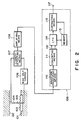
- Relativ-Positionserfassungsvorrichtung mit einer Sonde (104; 1701A; 5007; 5007′; 6007; 5071; 7102; 8102; 8601; 9001), die einen in einer ersten Richtung auf eine Referenz (101; 102; 5040; 7001; 8001; 8604; 9002) ausgerichteten Endabschnitt zur relativen Bewegung zwischen der Referenz und der Sonde in einer zweiten von der ersten Richtung unter-schiedlichen Richtung,
eine Vorrichtung (106, 1702A; 7106; Vp; V; 7113; 98008) zum Anlegen einer Spannung zwischen die Sonde und die Referenz und
eine Vorrichtung (107; 1703A; 7107; 5009; 6009; 7006; 8105; 9003) zum Erfassen eines zwischen der Sonde und der Referenz fließenden Tunnelstroms (105 Ip) aufweist,
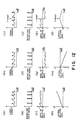
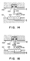
wobei eine nicht ringförmige gleichförmige Skala (103; 402; 403, 404; 1001; 5042; 6042) vorgesehen ist, welche sich in der zweiten Richtung erstreckt und wobei eine relative Position zwischen der Sonde und der Referenz auf der Grundlage der durch die Skala hervorgerufene Änderung im Tunnelstrom erfaßt wird. - Vorrichtung nach Patentanspruch 1,
wobei die Skala eine Anordnung von Atomen oder Molekülen (301) aufweist. - Vorrichtung nach Patentanspruch 1 oder 2, mit einer Vorrichtung (1901, 1902; 2801A, 2802A; 4115, 4116, 4117, 4118) zum Erfassen eines relativen Bewegungsabstandes zwischen der Sonde und der Referenz auf der Grundlage der durch die Skala während der relativen Bewegung hervorgerufenen Anzahl von Änderungen.
- Vorrichtung nach Patentanspruch 3,
wobei die Vorrichtung zum Erfassen des relativen Bewegungsabstands ein Stellglied (1901; 2801A; 4118; 5008b; 6008b; 7107, 7111) zum Bewegen der Sonde und der Referenz in der ersten Richtung, eine Vorrichtung (1902; 2802A; 4115, 4116, 4117; 7109, 7110) zum Erzeugen eines Ansteuersignals zum derartigen Steuern des Stellgliedes, das ein konstanter Tunnelstrom zwischen der Sonde und der Referenz fließt, eine Vorrichtung zum Weiterverarbeiten des Kurvensignals des Ansteuersignals und eine Vorrichtung zum Zählen der Signalwellen des verarbeiteten Kurvensignals aufweist. - Vorrichtung nach Patentanspruch 3, wobei die Vorrichtung zum Erfassen des relativen Bewegungsabstandes eine Vorrichtung zum Weiterverarbeiten des von der Tunnelstrom-Erfassungsvorrichtung erfaßten Tunnelstrom-Kurvensignals, und eine Vorrichtung zum Zählen der Signalwellen des weiterverarbeiteten Kurvensignals aufweist.
- Vorrichtung nach Patentanspruch 4 oder 5, wobei die Skala (403, 404; 1001) in der zweiten Richtung asymmetrisch ist, und ferner eine Vorrichtung (111) zum Erfassen der Richtung der relativen Bewegung zwischen der Sonde und der Referenz vorgesehen ist.
- Vorrichtung nach Patentanspruch 4 oder 5, mit einer Vorrichtung (1301; 1501) zum Eingeben von feinen Vibrationen in die Sonde in der zweiten Richtung, und einer Vorrichtung (111) zum Erfassen der Richtung der relativen Bewegung zwischen der Sonde und der Referenz.
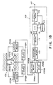
- Vorrichtung nach Patentanspruch 4, wobei eine zusätzliche Sonde (1701B; 5072; 7103; 8602), die einen in der ersten Richtung auf eine Referenz ausgerichteten Endabschnitt besitzt, zur relativen Bewegung zwischen der Referenz und der zusätzlichen Sonde in der zweiten Richtung gemeinsam mit der ersten Sonde,
eine Vorrichtung (1702B; 7113) zum Anlegen einer Spannung zwischen die zusätzliche Sonde und die Referenz,
eine zusätzliche Erfassungsvorrichtung (1703B; 7106; 8608) zum Erfassen eines zwischen der zusätzlichen Sonde und der Referenz fließenden Tunnelstroms,
ein zusätzliches Stellglied (2801B; 5082a; 7108; 8605P) zum Eingeben einer relativen Bewegung zwischen der Sonde und der Referenz in der ersten Bewegung,
eine Vorrichtung (2802B; 7109; 8608) zum Erzeugen eines Ansteuersignals zum Steuern des zusätzlichen Stellgliedes, wodurch ein zwischen der zusätzlichen Sonde und der Referenz fließender Tunnelstrom konstant gehalten wird,
eine Vorrichtung zum Weiterverarbeiten des Kurvensignals des Ansteuersignals, und
eine Vorrichtung (111) zum Erfassen einer Richtung der relativen Bewegung der ersten Sonde und der Referenz auf der Grundlage des Phasenunterschiedes zwischen dem ersten Ansteuersignal und des zusätzlichen Ansteuersignals vorgesehen ist. - Vorrichtung nach Patentanspruch 5, bestehend aus einer zusätzlichen Sonde mit einem in der ersten Richtung auf eine Referenz ausgerichteten Endabschnitt zum relativen Bewegen zwischen der Referenz und der zusätzlichen Sonde in der zweiten Richtung gemeinsam mit der ersten Sonde, einer Vorrichtung zum Anlegen einer Spannung zwischen die zusätzliche Sonde und die Referenz,
einer zusätzlichen Erfassungsvorrichtung zum Erfassen eines zwischen der zusätzlichen Sonde und der Referenz fließenden Tunnelstroms, und
einer Vorrichtung zum Erfassen einer Richtung der relativen Bewegung der ersten Sonde und der Referenz auf der Grundlage eines Phasenunterschiedes zwischen dem ersten Tunnelstrom und dem zusätzlichen Tunnelstrom. - Vorrichtung nach Patentanspruch 3, bestehend aus einer zusätzlichen Sonde mit einem in der ersten Richtung auf eine zusätzliche Referenz (8604B) ausgerichteten Endabschnitt zum relativen Bewegen zwischen der zusätzlichen Referenz und der zusätzlichen Sonde in der zweiten Richtung gemeinsam mit der ersten Sonde, wobei die zusätzliche Referenz einen Phasenunterschied in Bezug auf die erste Referenz (8604) aufweist.
- Vorrichtung nach Patentanspruch 3, wobei die Referenz eine zusätzliche gleichmäßige Skala aufweist, die sich in der zweiten Richtung mit einer größeren Gradeinteilung erstreckt.
- Vorrichtung nach Patentanspruch 3, bestehend aus einer zusätzlichen Referenz (5041), die sich in der zweiten Richtung erstreckt und die eine Skala mit einer größeren Gradeinteilung aufweist als die der ersten Skala (5042) und einer Photocodiereinrichtung (5003) zum Erfassen eines relativen Bewegungsabstandes eines auf die Sonde montierten Objektes in der zweiten Richtung, wobei die zusätzliche Referenz verwendet wird.
- Vorrichtung nach Patentanspruch 1, wobei die Referenz einen Bezugspunkt eines Ursprungs (501; 601a₁ bis 601a₃; 601b₁ bis 601b₃; 601c₁ bis 601c₃; 701d₁ bis 701d₄; 801; 802, 803, 804; 802′, 803′, 804; 7201; 7303; 8202; 8401, 8402; 8501, 8502) aufweist.
- Aufnahme- oder Wiedergabegerät mit einer Relativ-Positionserfassungsvorrichtung nach Patentanspruch 1 oder 2 , wobei die Referenz auf einem Aufzeichnungsmaterial (7001; 8001; 8604; 9002) vorgesehen ist, und die Informationen an einer gewünschten Position auf der Grundlage der mittels der relativen Positionserfassungsvorrichtung erfaßten relativ-Position aufgezeichnet oder wiedergegeben werden.
- Vorrichtung nach Patentanspruch 14, wobei die Informationen mittels der Sonde aufgezeichnet oder wiedergegeben werden.
- Vorrichtung nach Patentanspruch 14, bestehend aus einer zusätzlichen Sonde (8601) zum Durchführen einer Aufzeichnung oder Wiedergabe von Informationen auf oder von dem Aufzeichnungsmaterial.
Priority Applications (1)
| Application Number | Priority Date | Filing Date | Title |
|---|---|---|---|
| EP94120561A EP0646913B1 (de) | 1987-08-25 | 1988-08-24 | Tunnelstromkodierer |
Applications Claiming Priority (16)
| Application Number | Priority Date | Filing Date | Title |
|---|---|---|---|
| JP62212153A JP2603270B2 (ja) | 1987-08-25 | 1987-08-25 | 記録装置および再生装置 |
| JP212153/87 | 1987-08-25 | ||
| JP62212154A JP2632862B2 (ja) | 1987-08-25 | 1987-08-25 | 位置検出装置 |
| JP212154/87 | 1987-08-25 | ||
| JP62305748A JP2547334B2 (ja) | 1987-12-04 | 1987-12-04 | 位置検出装置 |
| JP62305747A JP2547333B2 (ja) | 1987-12-04 | 1987-12-04 | 位置検出装置 |
| JP305748/87 | 1987-12-04 | ||
| JP305747/87 | 1987-12-04 | ||
| JP309421/87 | 1987-12-09 | ||
| JP62309421A JP2559048B2 (ja) | 1987-12-09 | 1987-12-09 | 相対変位量測定装置 |
| JP201307/88 | 1988-08-12 | ||
| JP20130888A JP2692879B2 (ja) | 1988-08-12 | 1988-08-12 | 相対変位量測定装置 |
| JP201306/88 | 1988-08-12 | ||
| JP63201307A JP2851855B2 (ja) | 1988-08-12 | 1988-08-12 | 記録再生装置 |
| JP20130688A JP2670448B2 (ja) | 1988-08-12 | 1988-08-12 | 記録再生装置 |
| JP201308/88 | 1988-08-12 |
Related Child Applications (2)
| Application Number | Title | Priority Date | Filing Date |
|---|---|---|---|
| EP94120561A Division EP0646913B1 (de) | 1987-08-25 | 1988-08-24 | Tunnelstromkodierer |
| EP94120561.9 Division-Into | 1994-12-23 |
Publications (3)
| Publication Number | Publication Date |
|---|---|
| EP0304893A2 EP0304893A2 (de) | 1989-03-01 |
| EP0304893A3 EP0304893A3 (de) | 1993-04-07 |
| EP0304893B1 true EP0304893B1 (de) | 1995-07-19 |
Family
ID=27573426
Family Applications (2)
| Application Number | Title | Priority Date | Filing Date |
|---|---|---|---|
| EP94120561A Expired - Lifetime EP0646913B1 (de) | 1987-08-25 | 1988-08-24 | Tunnelstromkodierer |
| EP88113794A Expired - Lifetime EP0304893B1 (de) | 1987-08-25 | 1988-08-24 | Codiereinrichtung |
Family Applications Before (1)
| Application Number | Title | Priority Date | Filing Date |
|---|---|---|---|
| EP94120561A Expired - Lifetime EP0646913B1 (de) | 1987-08-25 | 1988-08-24 | Tunnelstromkodierer |
Country Status (3)
| Country | Link |
|---|---|
| US (2) | US5519686A (de) |
| EP (2) | EP0646913B1 (de) |
| DE (2) | DE3854173T2 (de) |
Families Citing this family (82)
| Publication number | Priority date | Publication date | Assignee | Title |
|---|---|---|---|---|
| DE3854173T2 (de) * | 1987-08-25 | 1995-11-30 | Canon Kk | Codiereinrichtung. |
| JP2714211B2 (ja) * | 1989-03-16 | 1998-02-16 | キヤノン株式会社 | 記録及び再生装置 |
| US5241527A (en) * | 1989-03-16 | 1993-08-31 | Canon Kabushiki Kaisha | Recording and reproducing apparatus and method using a recording layer having a positioning region |
| DE69002503T2 (de) * | 1989-03-29 | 1994-03-03 | Canon Kk | Kantendetektor. |
| US5304924A (en) * | 1989-03-29 | 1994-04-19 | Canon Kabushiki Kaisha | Edge detector |
| JP2775464B2 (ja) * | 1989-04-27 | 1998-07-16 | キヤノン株式会社 | 位置検出装置 |
| JP2686645B2 (ja) * | 1989-05-08 | 1997-12-08 | キヤノン株式会社 | 走査型トンネル電流検出装置 |
| EP0398334B1 (de) * | 1989-05-17 | 1994-09-21 | Canon Kabushiki Kaisha | Vorrichtung zur Ermittlung einer Position |
| DE3921756C1 (de) * | 1989-07-01 | 1991-01-03 | Teldix Gmbh, 6900 Heidelberg, De | |
| DE69024571T2 (de) * | 1989-09-07 | 1996-06-13 | Canon Kk | Informationsverarbeitungsverfahren und -vorrichtung |
| JP2996748B2 (ja) * | 1990-02-09 | 2000-01-11 | キヤノン株式会社 | 位置ずれ検出装置および方法 |
| JP2945090B2 (ja) * | 1990-07-09 | 1999-09-06 | キヤノン株式会社 | エンコーダ |
| US5441804A (en) * | 1991-02-12 | 1995-08-15 | Mitsubishi Plastics Industries Limited | Magneto-optical recording medium and method for production thereof |
| JP2983876B2 (ja) * | 1994-03-22 | 1999-11-29 | 徹雄 大原 | リアルタイムかつナノメータスケールの位置測定方法および装置 |
| US6353219B1 (en) | 1994-07-28 | 2002-03-05 | Victor B. Kley | Object inspection and/or modification system and method |
| US5751683A (en) * | 1995-07-24 | 1998-05-12 | General Nanotechnology, L.L.C. | Nanometer scale data storage device and associated positioning system |
| US6337479B1 (en) * | 1994-07-28 | 2002-01-08 | Victor B. Kley | Object inspection and/or modification system and method |
| US6339217B1 (en) * | 1995-07-28 | 2002-01-15 | General Nanotechnology Llc | Scanning probe microscope assembly and method for making spectrophotometric, near-field, and scanning probe measurements |
| JP3625530B2 (ja) * | 1995-06-12 | 2005-03-02 | ヒューレット・パッカード・カンパニー | 位置検出装置及び位置検出方法 |
| JPH0981977A (ja) * | 1995-07-10 | 1997-03-28 | Canon Inc | 記録再生装置 |
| US6507553B2 (en) | 1995-07-24 | 2003-01-14 | General Nanotechnology Llc | Nanometer scale data storage device and associated positioning system |
| US6011664A (en) * | 1995-08-31 | 2000-01-04 | Carnegie Mellon University | Techniques for ultrahigh density writing with a probe on erasable magnetic media |
| US5744799A (en) * | 1996-05-20 | 1998-04-28 | Ohara; Tetsuo | Apparatus for and method of real-time nanometer-scale position measurement of the sensor of a scanning tunneling microscope or other sensor scanning atomic or other undulating surfaces |
| US7102982B1 (en) * | 1997-05-30 | 2006-09-05 | International Business Machines Corporation | Storage apparatus and method utilizing a charge storage layer having discrete conductive charge-storing elements |
| US5856967A (en) * | 1997-08-27 | 1999-01-05 | International Business Machines Corporation | Atomic force microscopy data storage system with tracking servo from lateral force-sensing cantilever |
| US6195313B1 (en) * | 1997-08-29 | 2001-02-27 | Canon Kabushiki Kaisha | Tracking mechanism and method using probes for information recording/reproducing apparatus |
| US6923044B1 (en) | 2001-03-08 | 2005-08-02 | General Nanotechnology Llc | Active cantilever for nanomachining and metrology |
| US6787768B1 (en) | 2001-03-08 | 2004-09-07 | General Nanotechnology Llc | Method and apparatus for tool and tip design for nanomachining and measurement |
| US7196328B1 (en) | 2001-03-08 | 2007-03-27 | General Nanotechnology Llc | Nanomachining method and apparatus |
| US6802646B1 (en) * | 2001-04-30 | 2004-10-12 | General Nanotechnology Llc | Low-friction moving interfaces in micromachines and nanomachines |
| US6752008B1 (en) | 2001-03-08 | 2004-06-22 | General Nanotechnology Llc | Method and apparatus for scanning in scanning probe microscopy and presenting results |
| CN1249398C (zh) * | 1998-09-07 | 2006-04-05 | 坤特精密仪器有限公司 | 采用细长导电体之间的隧道效应电流的测量方法 |
| US7260051B1 (en) * | 1998-12-18 | 2007-08-21 | Nanochip, Inc. | Molecular memory medium and molecular memory integrated circuit |
| EP1196939A4 (de) * | 1999-07-01 | 2002-09-18 | Gen Nanotechnology Llc | Vorrichtung und verfahren zur untersuchung und/oder veränderungsobjekt |
| US8271316B2 (en) * | 1999-12-17 | 2012-09-18 | Buzzmetrics Ltd | Consumer to business data capturing system |
| US6931710B2 (en) * | 2001-01-30 | 2005-08-23 | General Nanotechnology Llc | Manufacturing of micro-objects such as miniature diamond tool tips |
| US7253407B1 (en) | 2001-03-08 | 2007-08-07 | General Nanotechnology Llc | Active cantilever for nanomachining and metrology |
| US6791931B2 (en) * | 2001-03-16 | 2004-09-14 | Hewlett-Packard Development Company, L.P. | Accelerometer using field emitter technology |
| US20020138301A1 (en) * | 2001-03-22 | 2002-09-26 | Thanos Karras | Integration of a portal into an application service provider data archive and/or web based viewer |
| US7053369B1 (en) | 2001-10-19 | 2006-05-30 | Rave Llc | Scan data collection for better overall data accuracy |
| US6813937B2 (en) | 2001-11-28 | 2004-11-09 | General Nanotechnology Llc | Method and apparatus for micromachines, microstructures, nanomachines and nanostructures |
| ATE338301T1 (de) | 2002-04-15 | 2006-09-15 | Epos Technologies Ltd | Verfahren und system zum erfassen von positionsdaten |
| JP4628099B2 (ja) * | 2002-07-08 | 2011-02-09 | マルチプローブ・インコーポレーテッド | 複数の走査プローブのソフトウエア同期化 |
| JP2005538855A (ja) | 2002-09-09 | 2005-12-22 | ジェネラル ナノテクノロジー エルエルシー | 走査型プローブ顕微鏡の流体送達 |
| US7233517B2 (en) * | 2002-10-15 | 2007-06-19 | Nanochip, Inc. | Atomic probes and media for high density data storage |
| US7133351B2 (en) * | 2003-08-01 | 2006-11-07 | Hewlett-Packard Development Company, L.P. | Data storage device and a method of reading data in a data storage device |
| KR100585462B1 (ko) * | 2003-12-26 | 2006-06-07 | 한국전자통신연구원 | 정보 저장 및 독출 장치 |
| US20050243592A1 (en) * | 2004-04-16 | 2005-11-03 | Rust Thomas F | High density data storage device having eraseable bit cells |
| US20050243660A1 (en) * | 2004-04-16 | 2005-11-03 | Rust Thomas F | Methods for erasing bit cells in a high density data storage device |
| WO2005111653A2 (en) | 2004-05-17 | 2005-11-24 | Epos Technologies Limited | Acoustic robust synchronization signaling for acoustic positioning system |
| US8391959B2 (en) * | 2004-09-29 | 2013-03-05 | Tel Hashomer Medical Research Infrastructure And Services Ltd. | Composition for improving efficiency of drug delivery |
| US7367944B2 (en) | 2004-12-13 | 2008-05-06 | Tel Hashomer Medical Research Infrastructure And Services Ltd. | Method and system for monitoring ablation of tissues |
| JP2006220560A (ja) * | 2005-02-10 | 2006-08-24 | Sii Nanotechnology Inc | 基板及び微小構造物並びに基準スケールの作製方法及び微小構造物の測長方法 |
| US7212488B2 (en) * | 2005-03-21 | 2007-05-01 | Hewlett-Packard Development Company, L.P. | Method and device enabling capacitive probe-based data storage readout |
| AU2006225986B2 (en) * | 2005-03-23 | 2011-09-01 | Qualcomm Incorporated | Method and system for digital pen assembly |
| US20070041237A1 (en) * | 2005-07-08 | 2007-02-22 | Nanochip, Inc. | Media for writing highly resolved domains |
| US7463573B2 (en) * | 2005-06-24 | 2008-12-09 | Nanochip, Inc. | Patterned media for a high density data storage device |
| US7367119B2 (en) * | 2005-06-24 | 2008-05-06 | Nanochip, Inc. | Method for forming a reinforced tip for a probe storage device |
| US20060291271A1 (en) * | 2005-06-24 | 2006-12-28 | Nanochip, Inc. | High density data storage devices having servo indicia formed in a patterned media |
| US20070008867A1 (en) * | 2005-07-08 | 2007-01-11 | Nanochip, Inc. | High density data storage devices with a lubricant layer comprised of a field of polymer chains |
| US20070008866A1 (en) * | 2005-07-08 | 2007-01-11 | Nanochip, Inc. | Methods for writing and reading in a polarity-dependent memory switch media |
| US20070008865A1 (en) * | 2005-07-08 | 2007-01-11 | Nanochip, Inc. | High density data storage devices with polarity-dependent memory switching media |
| DE102006021289B4 (de) * | 2006-05-05 | 2010-05-12 | Bundesrepublik Deutschland, vertr. d. d. Bundesministerium für Wirtschaft und Technologie, dieses vertr. d. d. Präsidenten der Physikalisch-Technischen Bundesanstalt | Verfahren und Vorrichtung zur Bestimmung einer Winkelteilung |
| US20080001075A1 (en) * | 2006-06-15 | 2008-01-03 | Nanochip, Inc. | Memory stage for a probe storage device |
| US20080175033A1 (en) * | 2007-01-19 | 2008-07-24 | Nanochip, Inc. | Method and system for improving domain stability in a ferroelectric media |
| US20080174918A1 (en) * | 2007-01-19 | 2008-07-24 | Nanochip, Inc. | Method and system for writing and reading a charge-trap media with a probe tip |
| NZ580288A (en) * | 2007-03-14 | 2012-07-27 | Epos Dev Ltd | A MEMS microphone including a case, a MEMS membrane, and a mesh covering |
| US20080233672A1 (en) * | 2007-03-20 | 2008-09-25 | Nanochip, Inc. | Method of integrating mems structures and cmos structures using oxide fusion bonding |
| US8031514B2 (en) * | 2007-04-09 | 2011-10-04 | Northeastern University | Bistable nanoswitch |
| WO2009013745A1 (en) * | 2007-07-23 | 2009-01-29 | Ramot At Tel Aviv University Ltd. | Photocatalytic hydrogen production and polypeptides capable of same |
| US20090129246A1 (en) * | 2007-11-21 | 2009-05-21 | Nanochip, Inc. | Environmental management of a probe storage device |
| US8347326B2 (en) | 2007-12-18 | 2013-01-01 | The Nielsen Company (US) | Identifying key media events and modeling causal relationships between key events and reported feelings |
| US20090294028A1 (en) * | 2008-06-03 | 2009-12-03 | Nanochip, Inc. | Process for fabricating high density storage device with high-temperature media |
| US20100039729A1 (en) * | 2008-08-14 | 2010-02-18 | Nanochip, Inc. | Package with integrated magnets for electromagnetically-actuated probe-storage device |
| US20100039919A1 (en) * | 2008-08-15 | 2010-02-18 | Nanochip, Inc. | Cantilever Structure for Use in Seek-and-Scan Probe Storage |
| JP5733724B2 (ja) * | 2009-06-23 | 2015-06-10 | 国立大学法人京都大学 | 走査型プローブ顕微鏡及びそのプローブ近接検出方法 |
| US20120109710A1 (en) * | 2010-10-27 | 2012-05-03 | Fair Isaac Corporation | Retail time to event scorecards incorporating clickstream data |
| JP5896804B2 (ja) * | 2012-03-26 | 2016-03-30 | 三菱電機株式会社 | リードヘッド制御機構、及び光学式エンコーダ |
| WO2014144018A2 (en) * | 2013-03-15 | 2014-09-18 | Bruker Nano, Inc. | Dual-probe scanning probe microscope |
| CN107636475A (zh) | 2015-02-26 | 2018-01-26 | 沙朗特有限责任公司 | 用于制造纳电子机械系统探针的系统和方法 |
| KR102097351B1 (ko) * | 2015-02-26 | 2020-04-06 | 살렌트, 엘엘씨 | 다중 통합 팁들 스캐닝 프로브 현미경 |
| KR20220067593A (ko) * | 2020-11-16 | 2022-05-25 | 삼성전자주식회사 | 근접장 검출용 프로브 및 이를 포함하는 근접장 검출 시스템 |
Family Cites Families (18)
| Publication number | Priority date | Publication date | Assignee | Title |
|---|---|---|---|---|
| US2715830A (en) * | 1952-07-12 | 1955-08-23 | Gen Motors Corp | Specimen for calibrating surface roughness measuring apparatus |
| CH643397A5 (de) * | 1979-09-20 | 1984-05-30 | Ibm | Raster-tunnelmikroskop. |
| US4575822A (en) * | 1983-02-15 | 1986-03-11 | The Board Of Trustees Of The Leland Stanford Junior University | Method and means for data storage using tunnel current data readout |
| US4560924A (en) * | 1983-07-22 | 1985-12-24 | Magnetic Peripherals Inc. | Flatness measuring apparatus |
| US4907195A (en) * | 1984-09-14 | 1990-03-06 | Xerox Corporation | Method of and system for atomic scale recording of information |
| US4677296A (en) * | 1984-09-24 | 1987-06-30 | Siemens Aktiengesellschaft | Apparatus and method for measuring lengths in a scanning particle microscope |
| US4618767A (en) * | 1985-03-22 | 1986-10-21 | International Business Machines Corporation | Low-energy scanning transmission electron microscope |
| US4724318A (en) * | 1985-11-26 | 1988-02-09 | International Business Machines Corporation | Atomic force microscope and method for imaging surfaces with atomic resolution |
| JPS62209302A (ja) * | 1986-03-10 | 1987-09-14 | Shimadzu Corp | 平行移動量検出装置 |
| EP0247219B1 (de) * | 1986-05-27 | 1991-05-15 | International Business Machines Corporation | Speichereinheit mit direktem Zugriff |
| EP0252745A3 (de) * | 1986-07-11 | 1990-01-24 | AGENCY OF INDUSTRIAL SCIENCE & TECHNOLOGY MINISTRY OF INTERNATIONAL TRADE & INDUSTRY | Gerät zum Steuern relativer Verschiebungen |
| US4877957A (en) * | 1986-07-14 | 1989-10-31 | Olympus Optical Co., Ltd. | Scanning type tunnel microscope |
| JPS63304103A (ja) * | 1987-06-05 | 1988-12-12 | Hitachi Ltd | 走査表面顕微鏡 |
| DE3854173T2 (de) * | 1987-08-25 | 1995-11-30 | Canon Kk | Codiereinrichtung. |
| US4814622A (en) * | 1987-11-06 | 1989-03-21 | Bell Communications Research, Inc. | High speed scanning tunneling microscope |
| US4916688A (en) * | 1988-03-31 | 1990-04-10 | International Business Machines Corporation | Data storage method using state transformable materials |
| US4987303A (en) * | 1989-04-07 | 1991-01-22 | Olympus Optical Co., Inc. | Micro-displacement detector device, piezo-actuator provided with the micro-displacement detector device and scanning probe microscope provided with the piezo-actuator |
| JP2775464B2 (ja) * | 1989-04-27 | 1998-07-16 | キヤノン株式会社 | 位置検出装置 |
-
1988
- 1988-08-24 DE DE3854173T patent/DE3854173T2/de not_active Expired - Fee Related
- 1988-08-24 DE DE3856296T patent/DE3856296T2/de not_active Expired - Fee Related
- 1988-08-24 EP EP94120561A patent/EP0646913B1/de not_active Expired - Lifetime
- 1988-08-24 EP EP88113794A patent/EP0304893B1/de not_active Expired - Lifetime
-
1995
- 1995-05-08 US US08/438,079 patent/US5519686A/en not_active Expired - Lifetime
-
1996
- 1996-01-22 US US08/589,473 patent/US5721721A/en not_active Expired - Fee Related
Also Published As
| Publication number | Publication date |
|---|---|
| EP0646913A3 (de) | 1996-08-21 |
| US5519686A (en) | 1996-05-21 |
| EP0304893A2 (de) | 1989-03-01 |
| DE3854173T2 (de) | 1995-11-30 |
| EP0304893A3 (de) | 1993-04-07 |
| DE3854173D1 (de) | 1995-08-24 |
| EP0646913B1 (de) | 1999-01-13 |
| EP0646913A2 (de) | 1995-04-05 |
| DE3856296D1 (de) | 1999-02-25 |
| DE3856296T2 (de) | 1999-07-15 |
| US5721721A (en) | 1998-02-24 |
Similar Documents
| Publication | Publication Date | Title |
|---|---|---|
| EP0304893B1 (de) | Codiereinrichtung | |
| CA1312952C (en) | Microprobe, preparation thereof and electronic device by use of said microprobe | |
| EP0416920B1 (de) | Informationsverarbeitungsverfahren und -vorrichtung | |
| US5317152A (en) | Cantilever type probe, and scanning tunnel microscope and information processing apparatus employing the same | |
| US5448421A (en) | Method for positioning an information processing head by detecting a magnetization pattern on a magnetic material positioned relative to a recording medium and a process for forming a recording and/or reproducing cantilever type probe | |
| KR100540027B1 (ko) | 원자간측정방법 | |
| EP0378444B1 (de) | Wiedergabegerät | |
| EP0475365B1 (de) | Nachführungsmethode für Speichergerät | |
| EP0674170A1 (de) | Interatomares Messverfahren | |
| US5132533A (en) | Method for forming probe and apparatus therefor | |
| CA1328131C (en) | Encoder | |
| US5793040A (en) | Information processing aparatus effecting probe position control with electrostatic force | |
| JP2603270B2 (ja) | 記録装置および再生装置 | |
| JP2000511634A (ja) | 原子間測定技術 | |
| EP0640963B1 (de) | Aufzeichnungs und Wiedergabeverfahren und Gerät mit einer Rastersonde | |
| EP0449409A2 (de) | Sonde, Vorrichtung zur Datenverarbeitung in welcher die Sonde benutzt wird und Verfahren zum Gebrauch und zur Herstellung | |
| JP2559048B2 (ja) | 相対変位量測定装置 | |
| JPH06333276A (ja) | 記録媒体及びその製造方法、及び該記録媒体を用いた情報処理装置 | |
| JP2632862B2 (ja) | 位置検出装置 | |
| JP2670448B2 (ja) | 記録再生装置 | |
| JP2686651B2 (ja) | 変位量検出装置 | |
| CA2045878C (en) | Method for forming probe and apparatus therefor | |
| CA2024725C (en) | Information processing method and information processing device | |
| JPH06162581A (ja) | 記録再生装置 | |
| JPH0490151A (ja) | 情報処理方法及び情報処理装置 |
Legal Events
| Date | Code | Title | Description |
|---|---|---|---|
| PUAI | Public reference made under article 153(3) epc to a published international application that has entered the european phase |
Free format text: ORIGINAL CODE: 0009012 |
|
| 17P | Request for examination filed |
Effective date: 19880824 |
|
| AK | Designated contracting states |
Kind code of ref document: A2 Designated state(s): BE CH DE FR GB IT LI NL SE |
|
| PUAL | Search report despatched |
Free format text: ORIGINAL CODE: 0009013 |
|
| AK | Designated contracting states |
Kind code of ref document: A3 Designated state(s): BE CH DE FR GB IT LI NL SE |
|
| 17Q | First examination report despatched |
Effective date: 19931129 |
|
| GRAA | (expected) grant |
Free format text: ORIGINAL CODE: 0009210 |
|
| AK | Designated contracting states |
Kind code of ref document: B1 Designated state(s): BE CH DE FR GB IT LI NL SE |
|
| XX | Miscellaneous (additional remarks) |
Free format text: TEILANMELDUNG 94120561.9 EINGEREICHT AM 24/08/88. |
|
| REF | Corresponds to: |
Ref document number: 3854173 Country of ref document: DE Date of ref document: 19950824 |
|
| ET | Fr: translation filed | ||
| ITF | It: translation for a ep patent filed |
Owner name: SOCIETA' ITALIANA BREVETTI S.P.A. |
|
| PLBE | No opposition filed within time limit |
Free format text: ORIGINAL CODE: 0009261 |
|
| STAA | Information on the status of an ep patent application or granted ep patent |
Free format text: STATUS: NO OPPOSITION FILED WITHIN TIME LIMIT |
|
| 26N | No opposition filed | ||
| REG | Reference to a national code |
Ref country code: GB Ref legal event code: IF02 |
|
| PGFP | Annual fee paid to national office [announced via postgrant information from national office to epo] |
Ref country code: SE Payment date: 20030806 Year of fee payment: 16 |
|
| PGFP | Annual fee paid to national office [announced via postgrant information from national office to epo] |
Ref country code: FR Payment date: 20030808 Year of fee payment: 16 |
|
| PGFP | Annual fee paid to national office [announced via postgrant information from national office to epo] |
Ref country code: GB Payment date: 20030820 Year of fee payment: 16 |
|
| PGFP | Annual fee paid to national office [announced via postgrant information from national office to epo] |
Ref country code: CH Payment date: 20030829 Year of fee payment: 16 |
|
| PGFP | Annual fee paid to national office [announced via postgrant information from national office to epo] |
Ref country code: NL Payment date: 20030831 Year of fee payment: 16 |
|
| PGFP | Annual fee paid to national office [announced via postgrant information from national office to epo] |
Ref country code: DE Payment date: 20030904 Year of fee payment: 16 |
|
| PGFP | Annual fee paid to national office [announced via postgrant information from national office to epo] |
Ref country code: BE Payment date: 20031009 Year of fee payment: 16 |
|
| PG25 | Lapsed in a contracting state [announced via postgrant information from national office to epo] |
Ref country code: GB Free format text: LAPSE BECAUSE OF NON-PAYMENT OF DUE FEES Effective date: 20040824 |
|
| PG25 | Lapsed in a contracting state [announced via postgrant information from national office to epo] |
Ref country code: SE Free format text: LAPSE BECAUSE OF NON-PAYMENT OF DUE FEES Effective date: 20040825 |
|
| PG25 | Lapsed in a contracting state [announced via postgrant information from national office to epo] |
Ref country code: LI Free format text: LAPSE BECAUSE OF NON-PAYMENT OF DUE FEES Effective date: 20040831 Ref country code: CH Free format text: LAPSE BECAUSE OF NON-PAYMENT OF DUE FEES Effective date: 20040831 Ref country code: BE Free format text: LAPSE BECAUSE OF NON-PAYMENT OF DUE FEES Effective date: 20040831 |
|
| BERE | Be: lapsed |
Owner name: *CANON K.K. Effective date: 20040831 |
|
| PG25 | Lapsed in a contracting state [announced via postgrant information from national office to epo] |
Ref country code: NL Free format text: LAPSE BECAUSE OF NON-PAYMENT OF DUE FEES Effective date: 20050301 Ref country code: DE Free format text: LAPSE BECAUSE OF NON-PAYMENT OF DUE FEES Effective date: 20050301 |
|
| EUG | Se: european patent has lapsed | ||
| GBPC | Gb: european patent ceased through non-payment of renewal fee |
Effective date: 20040824 |
|
| REG | Reference to a national code |
Ref country code: CH Ref legal event code: PL |
|
| PG25 | Lapsed in a contracting state [announced via postgrant information from national office to epo] |
Ref country code: FR Free format text: LAPSE BECAUSE OF NON-PAYMENT OF DUE FEES Effective date: 20050429 |
|
| NLV4 | Nl: lapsed or anulled due to non-payment of the annual fee |
Effective date: 20050301 |
|
| REG | Reference to a national code |
Ref country code: FR Ref legal event code: ST |
|
| PG25 | Lapsed in a contracting state [announced via postgrant information from national office to epo] |
Ref country code: IT Free format text: LAPSE BECAUSE OF NON-PAYMENT OF DUE FEES;WARNING: LAPSES OF ITALIAN PATENTS WITH EFFECTIVE DATE BEFORE 2007 MAY HAVE OCCURRED AT ANY TIME BEFORE 2007. THE CORRECT EFFECTIVE DATE MAY BE DIFFERENT FROM THE ONE RECORDED. Effective date: 20050824 |
|
| BERE | Be: lapsed |
Owner name: *CANON K.K. Effective date: 20040831 |