EP0300755A2 - Treiberschaltung - Google Patents
Treiberschaltung Download PDFInfo
- Publication number
- EP0300755A2 EP0300755A2 EP88306637A EP88306637A EP0300755A2 EP 0300755 A2 EP0300755 A2 EP 0300755A2 EP 88306637 A EP88306637 A EP 88306637A EP 88306637 A EP88306637 A EP 88306637A EP 0300755 A2 EP0300755 A2 EP 0300755A2
- Authority
- EP
- European Patent Office
- Prior art keywords
- waveform
- drive circuit
- voltage
- waveforms
- electrodes
- Prior art date
- Legal status (The legal status is an assumption and is not a legal conclusion. Google has not performed a legal analysis and makes no representation as to the accuracy of the status listed.)
- Granted
Links
- 239000004973 liquid crystal related substance Substances 0.000 claims description 24
- 238000000034 method Methods 0.000 claims description 10
- 210000002858 crystal cell Anatomy 0.000 claims description 3
- 239000000463 material Substances 0.000 description 7
- 230000000694 effects Effects 0.000 description 6
- 239000011159 matrix material Substances 0.000 description 6
- 230000005684 electric field Effects 0.000 description 5
- 239000005262 ferroelectric liquid crystals (FLCs) Substances 0.000 description 4
- 235000010290 biphenyl Nutrition 0.000 description 2
- 239000004305 biphenyl Substances 0.000 description 2
- -1 biphenyl ester Chemical class 0.000 description 2
- 239000003990 capacitor Substances 0.000 description 2
- 238000010586 diagram Methods 0.000 description 2
- 230000003287 optical effect Effects 0.000 description 2
- ZUOUZKKEUPVFJK-UHFFFAOYSA-N phenylbenzene Natural products C1=CC=CC=C1C1=CC=CC=C1 ZUOUZKKEUPVFJK-UHFFFAOYSA-N 0.000 description 2
- 101100041822 Schizosaccharomyces pombe (strain 972 / ATCC 24843) sce3 gene Proteins 0.000 description 1
- 239000004990 Smectic liquid crystal Substances 0.000 description 1
- 230000015556 catabolic process Effects 0.000 description 1
- 210000004027 cell Anatomy 0.000 description 1
- 230000001186 cumulative effect Effects 0.000 description 1
- 238000006731 degradation reaction Methods 0.000 description 1
- 239000011521 glass Substances 0.000 description 1
- 238000009413 insulation Methods 0.000 description 1
- 239000007788 liquid Substances 0.000 description 1
- 230000007774 longterm Effects 0.000 description 1
- 230000001151 other effect Effects 0.000 description 1
- 238000005070 sampling Methods 0.000 description 1
- 238000004088 simulation Methods 0.000 description 1
- 230000006641 stabilisation Effects 0.000 description 1
- 230000001360 synchronised effect Effects 0.000 description 1
Images


Classifications
-
- G—PHYSICS
- G09—EDUCATION; CRYPTOGRAPHY; DISPLAY; ADVERTISING; SEALS
- G09G—ARRANGEMENTS OR CIRCUITS FOR CONTROL OF INDICATING DEVICES USING STATIC MEANS TO PRESENT VARIABLE INFORMATION
- G09G3/00—Control arrangements or circuits, of interest only in connection with visual indicators other than cathode-ray tubes
- G09G3/20—Control arrangements or circuits, of interest only in connection with visual indicators other than cathode-ray tubes for presentation of an assembly of a number of characters, e.g. a page, by composing the assembly by combination of individual elements arranged in a matrix no fixed position being assigned to or needed to be assigned to the individual characters or partial characters
- G09G3/34—Control arrangements or circuits, of interest only in connection with visual indicators other than cathode-ray tubes for presentation of an assembly of a number of characters, e.g. a page, by composing the assembly by combination of individual elements arranged in a matrix no fixed position being assigned to or needed to be assigned to the individual characters or partial characters by control of light from an independent source
- G09G3/36—Control arrangements or circuits, of interest only in connection with visual indicators other than cathode-ray tubes for presentation of an assembly of a number of characters, e.g. a page, by composing the assembly by combination of individual elements arranged in a matrix no fixed position being assigned to or needed to be assigned to the individual characters or partial characters by control of light from an independent source using liquid crystals
- G09G3/3611—Control of matrices with row and column drivers
- G09G3/3685—Details of drivers for data electrodes
- G09G3/3692—Details of drivers for data electrodes suitable for passive matrices only
-
- G—PHYSICS
- G09—EDUCATION; CRYPTOGRAPHY; DISPLAY; ADVERTISING; SEALS
- G09G—ARRANGEMENTS OR CIRCUITS FOR CONTROL OF INDICATING DEVICES USING STATIC MEANS TO PRESENT VARIABLE INFORMATION
- G09G3/00—Control arrangements or circuits, of interest only in connection with visual indicators other than cathode-ray tubes
- G09G3/20—Control arrangements or circuits, of interest only in connection with visual indicators other than cathode-ray tubes for presentation of an assembly of a number of characters, e.g. a page, by composing the assembly by combination of individual elements arranged in a matrix no fixed position being assigned to or needed to be assigned to the individual characters or partial characters
- G09G3/34—Control arrangements or circuits, of interest only in connection with visual indicators other than cathode-ray tubes for presentation of an assembly of a number of characters, e.g. a page, by composing the assembly by combination of individual elements arranged in a matrix no fixed position being assigned to or needed to be assigned to the individual characters or partial characters by control of light from an independent source
- G09G3/36—Control arrangements or circuits, of interest only in connection with visual indicators other than cathode-ray tubes for presentation of an assembly of a number of characters, e.g. a page, by composing the assembly by combination of individual elements arranged in a matrix no fixed position being assigned to or needed to be assigned to the individual characters or partial characters by control of light from an independent source using liquid crystals
- G09G3/3611—Control of matrices with row and column drivers
- G09G3/3622—Control of matrices with row and column drivers using a passive matrix
- G09G3/3629—Control of matrices with row and column drivers using a passive matrix using liquid crystals having memory effects, e.g. ferroelectric liquid crystals
-
- G—PHYSICS
- G09—EDUCATION; CRYPTOGRAPHY; DISPLAY; ADVERTISING; SEALS
- G09G—ARRANGEMENTS OR CIRCUITS FOR CONTROL OF INDICATING DEVICES USING STATIC MEANS TO PRESENT VARIABLE INFORMATION
- G09G3/00—Control arrangements or circuits, of interest only in connection with visual indicators other than cathode-ray tubes
- G09G3/20—Control arrangements or circuits, of interest only in connection with visual indicators other than cathode-ray tubes for presentation of an assembly of a number of characters, e.g. a page, by composing the assembly by combination of individual elements arranged in a matrix no fixed position being assigned to or needed to be assigned to the individual characters or partial characters
- G09G3/34—Control arrangements or circuits, of interest only in connection with visual indicators other than cathode-ray tubes for presentation of an assembly of a number of characters, e.g. a page, by composing the assembly by combination of individual elements arranged in a matrix no fixed position being assigned to or needed to be assigned to the individual characters or partial characters by control of light from an independent source
- G09G3/36—Control arrangements or circuits, of interest only in connection with visual indicators other than cathode-ray tubes for presentation of an assembly of a number of characters, e.g. a page, by composing the assembly by combination of individual elements arranged in a matrix no fixed position being assigned to or needed to be assigned to the individual characters or partial characters by control of light from an independent source using liquid crystals
- G09G3/3611—Control of matrices with row and column drivers
- G09G3/3674—Details of drivers for scan electrodes
- G09G3/3681—Details of drivers for scan electrodes suitable for passive matrices only
-
- G—PHYSICS
- G09—EDUCATION; CRYPTOGRAPHY; DISPLAY; ADVERTISING; SEALS
- G09G—ARRANGEMENTS OR CIRCUITS FOR CONTROL OF INDICATING DEVICES USING STATIC MEANS TO PRESENT VARIABLE INFORMATION
- G09G2310/00—Command of the display device
- G09G2310/06—Details of flat display driving waveforms
-
- G—PHYSICS
- G09—EDUCATION; CRYPTOGRAPHY; DISPLAY; ADVERTISING; SEALS
- G09G—ARRANGEMENTS OR CIRCUITS FOR CONTROL OF INDICATING DEVICES USING STATIC MEANS TO PRESENT VARIABLE INFORMATION
- G09G2330/00—Aspects of power supply; Aspects of display protection and defect management
- G09G2330/02—Details of power systems and of start or stop of display operation
Definitions
- the invention relates to a drive circuit for producing a plurality of outputs, in particular, though not exclusively, to such a drive circuit for driving a matrix addressed display.
- the present invention concerns the use of readily-available integrated circuits for efficiently implementing complicated X-Y matrix display device drive schemes for two level displays.
- One application of the present invention is to techniques involving pulse-width multiplex switching of matrix-array type liquid crystal display devices, whether alone or in combination with pulse-height switching, as disclosed in our copending European Patent Application also claiming priority from GB 8717172 and GB 8718351.
- Another application of the present invention is to methods of addressing a matrix array type liquid crystal display device in which pixels not being switched are stabilised in a required state by the application of a high frequency A.C. waveform.
- Display driver chips are available which have multiple high voltage CMOS outputs and take the form of n stage shift registers with latched outputs. These chips were originally designed for use with ACEL displays but they are now being used in a number of LCD implementations. An apparent limitation of these devices is that the outputs are two state. The output voltage is either at the high voltage or at ground. This limitation is removed by using the proposed arrangement and method.
- a liquid crystal material consists of long thin polar molecules and so can preserve a high degree of long range orientational ordering of the molecules in a liquid condition.
- Such materials are anisotropic with properties, such as dielectric constant, characterised by two constants, one in the direction of the long molecular axis and one perpendicular to it.
- dielectric constant characterised by two constants, one in the direction of the long molecular axis and one perpendicular to it.
- the anisotropic nature of the dielectric constant enables the molecules to be aligned in an electric field, the molecules tending to be orientated in the direction giving the minimum electrostatic free energy.
- liquid crystal materials also exhibit ferroelectric properties i.e. they have a permanent dipole moment which is perpendicular to the long molecular axis.
- ferroelectric properties i.e. they have a permanent dipole moment which is perpendicular to the long molecular axis.
- the molecules When the liquid crystal material is placed between two glass plates whose surfaces have been treated to align the molecules, then the molecules will have two possible states depending on the direction of the permanent dipole moment. These states are bistable. By applying an electric field of the correct amplitude and polarity, it is possible to switch the molecules between the two states.
- the molecules Once the molecules have been switched into one of the two states, they can advantageously be stabilised in that state by the application of a high frequency A.C. waveform.
- the pixels of the matrix are defined by areas of overlap between members of a first set of electrodes on one side of the liquid crystal layer and members of a second set of electrodes on the other side of the liquid crystal layer.
- An electric field is applied across the molecules of a pixel by the generation of voltages at the member of the first set of electrodes and the member of the second set of electrodes that define the pixel.
- the individual electrodes can be either in electrical contact with or insulated from the liquid crystal layer.
- there is a risk of electrolytic degradation of the liquid crystal if there is a nett flow of direct current through the layer.
- an electric field has two effects on ferroelectric liquid crystal molecules.
- One is to stabilise them into the nearest preferred state by acting on the dielectric anisotropy.
- the applied couple due to this effect is proportional to the square of the voltage.
- the other effect of the field is to act on the permanent dipole.
- the couple applied due to this effect is proportional to the voltage.
- the nett effect is a parabolic voltage to 'switching force' characteristic.
- a drive circuit for producing a plurality of outputs suitable for driving a matrix-addressed display
- the circuit comprising a first and a second means to generate respectively a first and a second waveform, each of said first and said second means being capable of generating at least two voltage states, the instantaneous voltage of said first waveform being never less than that of said second waveform by more than a defined amount, the circuit further comprising a plurality of means to produce a respective output waveform by selectively switching to either said first waveform or said second waveform and means to control said selective switching, the arrangement being such that each of said plurality of means to produce a respective output waveform is capable of producing a respective output waveform having at least four voltage states.
- relatively complex output waveforms can be produced at a plurality of outputs but generating waveforms at only said first and said second means for the whole drive circuit.
- the invention utilises the fact that though the output waveform may be complex, involving four voltage states or more, and may be different at each output, at any one instant, an output should be in one of only two voltage states, depending on whether the output is to be 'on' or 'off'.
- the term 'slot' can have one of two meanings i.e. 1) the minimum time that a liquid crystal material takes to switch from a first state to a second state for a given pulse height; 2) the time for which a waveform is at a (given) constant voltage, i.e. the pulse width of a pulse of a given pulse height.
- meaning (2) is more common in the art, this will be the meaning intended in the present specification unless otherwise indicated. Also unless otherwise indicated the term used in the present specification for meaning (1) will be 'response time, t s '.
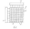
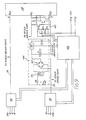
- Figure 1 shows, schematically, part of a matrix-array type liquid crystal cell 2 with a layer formed of a ferroelectric liquid crystal material, such as biphenyl ester sold under the trade name BDH SCE3, and having a thickness in the range of from 1.4 ⁇ m to 2.0 ⁇ m.
- the pixels 4 of the matrix are defined by areas of overlap between members of a first set of row electrodes 6 on one side of the liquid crystal layer and members of a second set of column electrodes 8 on the other side of the liquid crystal layer. For each pixel, the electric field thereacross determines the state and hence alignment of the liquid crystal molecules.
- Parallel polarizers (not shown) are provided at either side of the cell 2.
- each pixel has a first and a second optically distinguishable state provided by the two bistable states of the liquid crystal molecules in that pixel.
- Voltage waveforms are applied to the row electrodes 6 and column electrodes 8 respectively by row drivers 10 and column drivers 12.
- the matrix of pixels 4 is addressed on a line-by-line basis by applying voltage waveforms, termed strobe waveforms, serially to the row electrodes 6 while voltage waveforms, termed data waveforms, are applied in parallel to the column electrodes 8.
- the resultant waveform across a pixel defined by a row electrode and a column electrode is given by the potential difference between the waveform applied to that row electrode and the waveform applied to that column electrode.
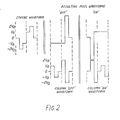
- Figure 2 shows an arrangement as disclosed in our copending European patent application also claiming priority from GB 8717172 and GB 8718351.
- the arrangment utilizes a 1.5 slot in the sense of a slot being the minimum time that the material takes to switch, i.e. 1.5t s .
- the driver output voltages have to change 6 times and 5 output states are required.
- the top left hand strobe waveform appears on the selected row. Unselected i,e, unstrobed rows have a constant 0 volts applied.
- the second row on the diagram shows the column or data waveforms. These have been arranged to consist of bipolar pulses to minimize their switching effect on unselected rows.
- the resultant pixel waveforms for a selected row are shown above the respective column waveforms.
- a pixel being switched off receives a long low voltage negative pulse followed by a short high voltage positive one of equivalent area maintaining zero D.C. content.
- a pixel being switched on receives a short high voltage negative equalising pulse followed by a long low voltage positive switching pulse.
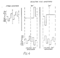
- Related schemes are shown in Figures 3 and 4 giving alternative equalisation pulse shapes.
- Figure 5 shows a one field three slot scheme arrangment including high frequency A.C. stabilisation.
- a pixel is switched by a pulse of height ⁇ 3V e and width t s .
- This switching pulse is charged balanced by two pulses of width t s , a first pulse of height ⁇ 2V e and a second pulse of average height ⁇ V e .
- These resulting pixel waveforms, as shown in Figures 5c and 5f are produced by the combination of a strobe waveform, as shown in Figure 5c and one of the column waveforms, respectively as shown in Figures 5a and 5b.
- the resulting pixel waveforms on unstrobed rows are shown in Figures 5g and 5h, the pixels of the unstrobed rows being A.C. stabilised.
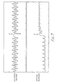
- Figures 6 and 7 show an oscilloscope trace of the switching voltage, i.e. resulting pixel waveform, and optical response resulting from a simulation of a waveform arrangement similar to that of Figure 2.
- Figure 6 shows that the liquid crystal is switching between the two optically distinguishable states and remaining stable while the row is not being selected; the switching waveform is too fast for the oscilloscope sampling.
- Figure 7 shows in more detail the switching point S. Switching occurs when the wide pulse is applied. The narrower equalisation and crosstalk pulses serve to stabilise the pixel state.
- FIG. 8 shows a block diagram representing a drive circuit provided in accordance with the present invention.
- the drive circuit comprises means 20 to generate a first waveform A at a first supply rail 21 and means 22 to generate a second waveform B at a second supply rail 23 which acts as ground potential for the circuit.
- a display driver chip 24 has a plurality of outputs, each including a switch for switching the output either to waveform A at the first supply rail 21 or to waveform B at the second supply rail 23. Accordingly a respective output waveform is produced at each of the plurality of outputs.
- each output to either waveform A or two waveform B is controlled by control and output latch data from a control circuit (not shown).
- the data is fed to the driver chip 24 via means to isolate the data waveforms so that these will be relative to the supply rail 23, such as opto-isolators 26. If the logic for an output is '1' then the output is switched to waveform A at supply rail 21; if the logic is '0' then the output is switched to waveform B at supply rail 23.
- the power supply to the driver chip 24 comprises an isolated power supply 28 to provide a constant 12V potential difference with respect to the potential of the ground supply rail 23.
- Waveforms X and Y at supply rails 30 and 32 are generated by first and second 4-way high voltage multiplexers 34, 36.
- Each multiplexer 34, 36 is capable of generating four voltage states, e.g.
- the display driver chip 38 of the circuit is an Si 9555 (manufactured under the trade mark 'Siliconix') having 32 channels, i.e. a 32 bit stage shift register, 32 latches and 32 outputs. Each one of the outputs is switched to either the voltage of supply rail 30 (i.e. waveform X) by a logic input of '1' or to the voltage of supply rail 32 (i.e. waveform Y) by a logic input of 'O'.
- FIG. 9 shows three outputs from the gate array 40 connected to respective three inputs of the driver chip 38 via three opto-isolators (designated generally by the reference 42).
- the three inputs shown comprise a clock input and a data input which load logic serially into the 32 bit stage shift register, and a latch enable which, when high, shifts the contents of the 32 bit stage shift register into an output register, in known manner Power is supplied to the gate array 40 itself by two supply rails at -2V f and -2V f + 5V.
- the driver chip 38 is powered by a 12V constant DC supply produced by an isolated power supply 44 connected across a positive power supply rail 45 and the ground supply rail 32.
- Inputs 46, 48 to the power supply 44 are connected to a 240V AC mains supply.
- the voltage is transformed down at a transformer 50 and rectified at a full wave rectifier 52.
- the power supply 44 further comprises a 10,000 ⁇ F electrolytic capacitor C1, a 7812 voltage regulator 54 and a 100nF capacitor C2.
- the 12V constant DC supply produced is constant with respect to the ground supply rail 32 and accordingly the positive power supply rail 45 has superimposed thereon the voltage of waveform Y.
- a typical display device has of the order of several hundred row and column electrodes and accordingly a large number of driver chips are required.
- a single multiplexer 34, multiplexer 36, isolated power supply 44 and gate array 40 can be provided for a set of row or column electrodes and corresponding driver chips.
- the chip is effectively being used as a set of analogue switches.
- the latches and the shift register are powered separately to the high voltage output stage so their operation is not affected, provided the power is maintained with respect to the ground (waveform B).
- Any of the outputs can be switched to either waveform A or waveform B.
- the only limitation is that the instantaneous voltage of waveform A must never be less than that of waveform B by more than two diode forward voltage drops. If the two alternative row or column drive waveforms cross then the contents of the output latches can be inverted and the waveforms interchanged.
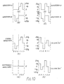
- Figure 10 shows how this method and arrangement can be used to implement the arrangement of Figure 3.
- the left hand column shows the waveforms for a drive circuit for the row electrodes and the right hand column shows the waveforms for a drive circuit for the column electrodes.
- Figures 10a and 10b show the waveforms A and B (both requiring three voltage states) applied to the supply rails of the row drive circuit.
- the strobed waveform ( Figure 10c) is produced by a data sequence of 000111 and the unstrobed waveform ( Figure 10d) by a data sequence of 111000. Accordingly the outputs of the row drive circuit are capable of producing respective output waveforms having five voltage states.
- Figures 10e and 10f show the waveforms A and B (both requiring three voltage states) applied to the supply rails of the column drive circuit.
- the column 'on' waveforms ( Figure 10g) is produced by a data sequence of 110011 and the column 'off' waveform ( Figure 10h) by a data sequence of 001100. Accordingly the outputs of the column drive circuit are capable of producing respective output waveforms having five voltage states.
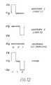
- FIG. 11 A second specific embodiment of a drive circuit is shown in Figure 11. This drive circuit is similar to that of Figure 9 and accordingly like parts are designated by like reference numerals.
- each output of the drive circuit needs to be capable of generating +2V e , -2V e and also the two ⁇ V g voltage states of the high frequency A.C. waveform of period t s /5, a total of four voltage states in all.
- t s is in the range of from 10 ⁇ s to 100 ⁇ s and so the high frequency AC waveform has a frequency of in the range of about 50KHz to about 500KHz.
- waveform generators 60, 62 produce waveforms C and D as shown in Figure 12. As shown in Figure 12, the waveforms are produced by selective switching, using a data sequence of 110 for the strobe waveform and data sequence of 001 for the A.C. stabilised waveform (for unstrobed rows).
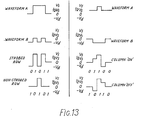
- Figure 13 shows an example of how this method and arrangement can be used to implement the five-slot coincident pulse scheme for a smectic C LC displays.
- the top four waveforms are those which would appear on the power lines to the respective driver chips.
- the lower four waveforms are those which appear on outputs that are cycled through the given data sequences.
Priority Applications (1)
| Application Number | Priority Date | Filing Date | Title |
|---|---|---|---|
| AT88306637T ATE96240T1 (de) | 1987-07-21 | 1988-07-20 | Treiberschaltung. |
Applications Claiming Priority (4)
| Application Number | Priority Date | Filing Date | Title |
|---|---|---|---|
| GB8717172 | 1987-07-21 | ||
| GB878717172A GB8717172D0 (en) | 1987-07-21 | 1987-07-21 | Display device |
| GB878718351A GB8718351D0 (en) | 1987-08-03 | 1987-08-03 | Display device |
| GB8718351 | 1987-08-03 |
Publications (3)
| Publication Number | Publication Date |
|---|---|
| EP0300755A2 true EP0300755A2 (de) | 1989-01-25 |
| EP0300755A3 EP0300755A3 (en) | 1990-06-13 |
| EP0300755B1 EP0300755B1 (de) | 1993-10-20 |
Family
ID=26292517
Family Applications (2)
| Application Number | Title | Priority Date | Filing Date |
|---|---|---|---|
| EP88306637A Expired - Lifetime EP0300755B1 (de) | 1987-07-21 | 1988-07-20 | Treiberschaltung |
| EP88306636A Expired - Lifetime EP0300754B1 (de) | 1987-07-21 | 1988-07-20 | Anzeigegerät |
Family Applications After (1)
| Application Number | Title | Priority Date | Filing Date |
|---|---|---|---|
| EP88306636A Expired - Lifetime EP0300754B1 (de) | 1987-07-21 | 1988-07-20 | Anzeigegerät |
Country Status (6)
| Country | Link |
|---|---|
| US (2) | US5010328A (de) |
| EP (2) | EP0300755B1 (de) |
| JP (2) | JP2609690B2 (de) |
| CA (2) | CA1311319C (de) |
| DE (2) | DE3886290T2 (de) |
| ES (2) | ES2047551T3 (de) |
Cited By (5)
| Publication number | Priority date | Publication date | Assignee | Title |
|---|---|---|---|---|
| EP0391655A2 (de) * | 1989-04-04 | 1990-10-10 | Sharp Kabushiki Kaisha | Ansteuerschaltung für ein Matrixanzeigegerät mit Flüssigkristallen |
| EP0762377A2 (de) * | 1995-08-18 | 1997-03-12 | Sony Corporation | Ansteuerungsverfahren für eine Flüssigkristallvorrichtung |
| EP0866441A1 (de) * | 1993-02-25 | 1998-09-23 | Seiko Epson Corporation | Steuerungsverfahren für Flüssigkristallanzeigeeinrichtung mit 8 Spannungspegeln |
| US6072558A (en) * | 1992-07-16 | 2000-06-06 | Seiko Epson Corporation | Electrooptical element switchable between a plurality of metabstable states |
| US6252571B1 (en) | 1995-05-17 | 2001-06-26 | Seiko Epson Corporation | Liquid crystal display device and its drive method and the drive circuit and power supply circuit device used therein |
Families Citing this family (48)
| Publication number | Priority date | Publication date | Assignee | Title |
|---|---|---|---|---|
| JPH02135419A (ja) * | 1988-11-17 | 1990-05-24 | Seiko Epson Corp | 液晶表示装置の駆動法 |
| US5301047A (en) * | 1989-05-17 | 1994-04-05 | Hitachi, Ltd. | Liquid crystal display |
| DE4017893A1 (de) * | 1990-06-02 | 1991-12-05 | Hoechst Ag | Verfahren zur ansteuerung eines ferroelektrischen fluessigkristalldisplays |
| JPH04113314A (ja) * | 1990-09-03 | 1992-04-14 | Sharp Corp | 液晶表示装置 |
| US6778159B1 (en) * | 1991-10-08 | 2004-08-17 | Semiconductor Energy Laboratory Co., Ltd. | Active matrix display and a method of driving the same |
| JP2639764B2 (ja) * | 1991-10-08 | 1997-08-13 | 株式会社半導体エネルギー研究所 | 電気光学装置の表示方法 |
| JP2639763B2 (ja) * | 1991-10-08 | 1997-08-13 | 株式会社半導体エネルギー研究所 | 電気光学装置およびその表示方法 |
| DE69411223T2 (de) * | 1993-04-30 | 1999-02-18 | Ibm | Verfahren und Vorrichtung zum Eliminieren des Übersprechens in einer Flüssigkristall-Anzeigeeinrichtung mit aktiver Matrix |
| US5517251A (en) * | 1994-04-28 | 1996-05-14 | The Regents Of The University Of California | Acquisition of video images simultaneously with analog signals |
| TW396200B (en) | 1994-10-19 | 2000-07-01 | Sumitomo Chemical Co | Liquid crystal composition and liquid crystal element containing such composition |
| JP3511409B2 (ja) * | 1994-10-27 | 2004-03-29 | 株式会社半導体エネルギー研究所 | アクティブマトリクス型液晶表示装置およびその駆動方法 |
| US5760759A (en) * | 1994-11-08 | 1998-06-02 | Sanyo Electric Co., Ltd. | Liquid crystal display |
| KR970700896A (ko) * | 1994-11-28 | 1997-02-12 | 요트.게.아. 롤페즈 | 액정 표시 장치 접속용 마이크로 콘트롤러 장치(Microcontroller interfacing with an LCD) |
| US5739805A (en) * | 1994-12-15 | 1998-04-14 | David Sarnoff Research Center, Inc. | Matrix addressed LCD display having LCD age indication, and autocalibrated amplification driver, and a cascaded column driver with capacitor-DAC operating on split groups of data bits |
| CN1129887C (zh) * | 1994-12-26 | 2003-12-03 | 夏普公司 | 液晶显示装置 |
| WO1999052006A2 (en) | 1998-04-08 | 1999-10-14 | Etalon, Inc. | Interferometric modulation of radiation |
| US8928967B2 (en) | 1998-04-08 | 2015-01-06 | Qualcomm Mems Technologies, Inc. | Method and device for modulating light |
| ES2143883T3 (es) | 1998-04-17 | 2000-05-16 | Barco Nv | Conversion de una señal de video para accionar una pantalla de cristal liquido. |
| JP2006047997A (ja) * | 2004-06-30 | 2006-02-16 | Canon Inc | 変調回路、駆動回路および出力方法 |
| US7889163B2 (en) | 2004-08-27 | 2011-02-15 | Qualcomm Mems Technologies, Inc. | Drive method for MEMS devices |
| US7499208B2 (en) | 2004-08-27 | 2009-03-03 | Udc, Llc | Current mode display driver circuit realization feature |
| US7532195B2 (en) | 2004-09-27 | 2009-05-12 | Idc, Llc | Method and system for reducing power consumption in a display |
| US8514169B2 (en) | 2004-09-27 | 2013-08-20 | Qualcomm Mems Technologies, Inc. | Apparatus and system for writing data to electromechanical display elements |
| US7136213B2 (en) | 2004-09-27 | 2006-11-14 | Idc, Llc | Interferometric modulators having charge persistence |
| US7843410B2 (en) | 2004-09-27 | 2010-11-30 | Qualcomm Mems Technologies, Inc. | Method and device for electrically programmable display |
| US8878825B2 (en) | 2004-09-27 | 2014-11-04 | Qualcomm Mems Technologies, Inc. | System and method for providing a variable refresh rate of an interferometric modulator display |
| US7675669B2 (en) | 2004-09-27 | 2010-03-09 | Qualcomm Mems Technologies, Inc. | Method and system for driving interferometric modulators |
| US7679627B2 (en) | 2004-09-27 | 2010-03-16 | Qualcomm Mems Technologies, Inc. | Controller and driver features for bi-stable display |
| US8310441B2 (en) | 2004-09-27 | 2012-11-13 | Qualcomm Mems Technologies, Inc. | Method and system for writing data to MEMS display elements |
| US7724993B2 (en) | 2004-09-27 | 2010-05-25 | Qualcomm Mems Technologies, Inc. | MEMS switches with deforming membranes |
| US7545550B2 (en) | 2004-09-27 | 2009-06-09 | Idc, Llc | Systems and methods of actuating MEMS display elements |
| US7948457B2 (en) | 2005-05-05 | 2011-05-24 | Qualcomm Mems Technologies, Inc. | Systems and methods of actuating MEMS display elements |
| US7920136B2 (en) | 2005-05-05 | 2011-04-05 | Qualcomm Mems Technologies, Inc. | System and method of driving a MEMS display device |
| KR20080027236A (ko) | 2005-05-05 | 2008-03-26 | 콸콤 인코포레이티드 | 다이나믹 드라이버 ic 및 디스플레이 패널 구성 |
| US8391630B2 (en) | 2005-12-22 | 2013-03-05 | Qualcomm Mems Technologies, Inc. | System and method for power reduction when decompressing video streams for interferometric modulator displays |
| US7916980B2 (en) | 2006-01-13 | 2011-03-29 | Qualcomm Mems Technologies, Inc. | Interconnect structure for MEMS device |
| US8194056B2 (en) | 2006-02-09 | 2012-06-05 | Qualcomm Mems Technologies Inc. | Method and system for writing data to MEMS display elements |
| US7952545B2 (en) | 2006-04-06 | 2011-05-31 | Lockheed Martin Corporation | Compensation for display device flicker |
| US8049713B2 (en) | 2006-04-24 | 2011-11-01 | Qualcomm Mems Technologies, Inc. | Power consumption optimized display update |
| US7702192B2 (en) | 2006-06-21 | 2010-04-20 | Qualcomm Mems Technologies, Inc. | Systems and methods for driving MEMS display |
| US7777715B2 (en) | 2006-06-29 | 2010-08-17 | Qualcomm Mems Technologies, Inc. | Passive circuits for de-multiplexing display inputs |
| US7957589B2 (en) | 2007-01-25 | 2011-06-07 | Qualcomm Mems Technologies, Inc. | Arbitrary power function using logarithm lookup table |
| KR101487738B1 (ko) * | 2007-07-13 | 2015-01-29 | 삼성디스플레이 주식회사 | 액정 표시 장치 및 그의 구동 방법 |
| CN101562428B (zh) * | 2008-04-16 | 2011-06-15 | 瑞铭科技股份有限公司 | 信号调变装置及其控制方法 |
| US8405649B2 (en) | 2009-03-27 | 2013-03-26 | Qualcomm Mems Technologies, Inc. | Low voltage driver scheme for interferometric modulators |
| US8736590B2 (en) | 2009-03-27 | 2014-05-27 | Qualcomm Mems Technologies, Inc. | Low voltage driver scheme for interferometric modulators |
| US8669926B2 (en) | 2011-11-30 | 2014-03-11 | Qualcomm Mems Technologies, Inc. | Drive scheme for a display |
| KR101673733B1 (ko) * | 2012-02-27 | 2016-11-08 | 시웅-쾅 차이 | 데이터 전송 시스템 |
Citations (1)
| Publication number | Priority date | Publication date | Assignee | Title |
|---|---|---|---|---|
| EP0214856A2 (de) * | 1985-09-06 | 1987-03-18 | Matsushita Electric Industrial Co., Ltd. | Verfahren zur Ansteuerung eines Flüssigkristallrasterbildschirmes |
Family Cites Families (20)
| Publication number | Priority date | Publication date | Assignee | Title |
|---|---|---|---|---|
| US3911421A (en) * | 1973-12-28 | 1975-10-07 | Ibm | Selection system for matrix displays requiring AC drive waveforms |
| JPS51132940A (en) * | 1975-05-14 | 1976-11-18 | Sharp Corp | Electric source apparatus |
| JPS5227400A (en) * | 1975-08-27 | 1977-03-01 | Sharp Corp | Power source device |
| US4227193A (en) * | 1977-07-26 | 1980-10-07 | National Research Development Corporation | Method and apparatus for matrix addressing opto-electric displays |
| NL169647B (nl) * | 1977-10-27 | 1982-03-01 | Philips Nv | Weergeefinrichting met een vloeibaar kristal. |
| JPS54132196A (en) * | 1978-04-06 | 1979-10-13 | Seiko Instr & Electronics Ltd | Driving system for display unit |
| US4408135A (en) * | 1979-12-26 | 1983-10-04 | Tokyo Shibaura Denki Kabushiki Kaisha | Multi-level signal generating circuit |
| JPS5865481A (ja) * | 1981-10-15 | 1983-04-19 | 株式会社東芝 | 液晶駆動用電圧分割回路 |
| JPS5888788A (ja) * | 1981-11-24 | 1983-05-26 | 株式会社日立製作所 | 液晶表示装置 |
| JPS58216289A (ja) * | 1982-06-10 | 1983-12-15 | シャープ株式会社 | 液晶表示装置駆動回路 |
| GB2146473B (en) * | 1983-09-10 | 1987-03-11 | Standard Telephones Cables Ltd | Addressing liquid crystal displays |
| JPS61156229A (ja) * | 1984-12-28 | 1986-07-15 | Canon Inc | 液晶装置 |
| GB2173336B (en) * | 1985-04-03 | 1988-04-27 | Stc Plc | Addressing liquid crystal cells |
| GB2173337B (en) * | 1985-04-03 | 1989-01-11 | Stc Plc | Addressing liquid crystal cells |
| GB2173335B (en) * | 1985-04-03 | 1988-02-17 | Stc Plc | Addressing liquid crystal cells |
| JPS61241731A (ja) * | 1985-04-19 | 1986-10-28 | Seiko Instr & Electronics Ltd | スメクテイック液晶装置 |
| US4770502A (en) * | 1986-01-10 | 1988-09-13 | Hitachi, Ltd. | Ferroelectric liquid crystal matrix driving apparatus and method |
| JPS62218943A (ja) * | 1986-03-19 | 1987-09-26 | Sharp Corp | 液晶表示装置 |
| GB2194663B (en) * | 1986-07-18 | 1990-06-20 | Stc Plc | Display device |
| JP2505756B2 (ja) * | 1986-07-22 | 1996-06-12 | キヤノン株式会社 | 光学変調素子の駆動法 |
-
1988
- 1988-07-18 US US07/220,316 patent/US5010328A/en not_active Expired - Lifetime
- 1988-07-20 DE DE3886290T patent/DE3886290T2/de not_active Expired - Fee Related
- 1988-07-20 EP EP88306637A patent/EP0300755B1/de not_active Expired - Lifetime
- 1988-07-20 ES ES88306636T patent/ES2047551T3/es not_active Expired - Lifetime
- 1988-07-20 EP EP88306636A patent/EP0300754B1/de not_active Expired - Lifetime
- 1988-07-20 JP JP63179276A patent/JP2609690B2/ja not_active Expired - Fee Related
- 1988-07-20 CA CA000572581A patent/CA1311319C/en not_active Expired - Lifetime
- 1988-07-20 JP JP63179275A patent/JP2558331B2/ja not_active Expired - Fee Related
- 1988-07-20 CA CA000572574A patent/CA1311318C/en not_active Expired - Lifetime
- 1988-07-20 DE DE88306637T patent/DE3885026T2/de not_active Expired - Fee Related
- 1988-07-20 ES ES198888306637T patent/ES2046302T3/es not_active Expired - Lifetime
-
1991
- 1991-02-11 US US07/653,759 patent/US5111319A/en not_active Expired - Fee Related
Patent Citations (1)
| Publication number | Priority date | Publication date | Assignee | Title |
|---|---|---|---|---|
| EP0214856A2 (de) * | 1985-09-06 | 1987-03-18 | Matsushita Electric Industrial Co., Ltd. | Verfahren zur Ansteuerung eines Flüssigkristallrasterbildschirmes |
Non-Patent Citations (1)
| Title |
|---|
| DISPLAYS, vol. 6, no. 3, July 1985, Guildford, GB, pages 153-156; B. PIEPER: "Floating drive schemes for dual-frequency addressing of complex liquid crystal displays" * |
Cited By (9)
| Publication number | Priority date | Publication date | Assignee | Title |
|---|---|---|---|---|
| EP0391655A2 (de) * | 1989-04-04 | 1990-10-10 | Sharp Kabushiki Kaisha | Ansteuerschaltung für ein Matrixanzeigegerät mit Flüssigkristallen |
| EP0391655A3 (de) * | 1989-04-04 | 1992-09-09 | Sharp Kabushiki Kaisha | Ansteuerschaltung für ein Matrixanzeigegerät mit Flüssigkristallen |
| US5414443A (en) * | 1989-04-04 | 1995-05-09 | Sharp Kabushiki Kaisha | Drive device for driving a matrix-type LCD apparatus |
| US6072558A (en) * | 1992-07-16 | 2000-06-06 | Seiko Epson Corporation | Electrooptical element switchable between a plurality of metabstable states |
| EP0866441A1 (de) * | 1993-02-25 | 1998-09-23 | Seiko Epson Corporation | Steuerungsverfahren für Flüssigkristallanzeigeeinrichtung mit 8 Spannungspegeln |
| US6236385B1 (en) | 1993-02-25 | 2001-05-22 | Seiko Epson Corporation | Method of driving a liquid crystal display device |
| US6252571B1 (en) | 1995-05-17 | 2001-06-26 | Seiko Epson Corporation | Liquid crystal display device and its drive method and the drive circuit and power supply circuit device used therein |
| EP0762377A2 (de) * | 1995-08-18 | 1997-03-12 | Sony Corporation | Ansteuerungsverfahren für eine Flüssigkristallvorrichtung |
| EP0762377A3 (de) * | 1995-08-18 | 1997-12-03 | Sony Corporation | Ansteuerungsverfahren für eine Flüssigkristallvorrichtung |
Also Published As
| Publication number | Publication date |
|---|---|
| JPS6454421A (en) | 1989-03-01 |
| EP0300755B1 (de) | 1993-10-20 |
| DE3886290T2 (de) | 1994-06-09 |
| JPS6448042A (en) | 1989-02-22 |
| CA1311318C (en) | 1992-12-08 |
| US5010328A (en) | 1991-04-23 |
| DE3886290D1 (de) | 1994-01-27 |
| EP0300755A3 (en) | 1990-06-13 |
| DE3885026D1 (de) | 1993-11-25 |
| ES2047551T3 (es) | 1994-03-01 |
| DE3885026T2 (de) | 1994-04-28 |
| EP0300754B1 (de) | 1993-12-15 |
| JP2558331B2 (ja) | 1996-11-27 |
| CA1311319C (en) | 1992-12-08 |
| EP0300754A2 (de) | 1989-01-25 |
| JP2609690B2 (ja) | 1997-05-14 |
| US5111319A (en) | 1992-05-05 |
| EP0300754A3 (en) | 1990-06-13 |
| ES2046302T3 (es) | 1994-02-01 |
Similar Documents
| Publication | Publication Date | Title |
|---|---|---|
| EP0300755B1 (de) | Treiberschaltung | |
| US4707692A (en) | Electroluminescent display drive system | |
| KR100719274B1 (ko) | 액정 디스플레이용 누진 구동장치 및 구동방법 | |
| EP0224243A2 (de) | Optische Modulationsvorrichtung und Verfahren zu deren Ansteuerung | |
| EP0177365A2 (de) | Flüssigkristallanzeigevorrichtung für Zeitmultiplexansteuerung | |
| WO1995026545A1 (en) | Active matrix display device and method of driving such | |
| US7724221B2 (en) | Bistable nematic liquid crystal display method and device | |
| JPH11505635A (ja) | 表示装置 | |
| EP0350934B1 (de) | Flüssigkristallanzeigegerät | |
| EP0469531B1 (de) | Flüssigkristallgerät und Verfahren zum Steuern dieses Gerätes | |
| JP2759589B2 (ja) | 強誘電性液晶表示素子 | |
| CN101981495B (zh) | 胆甾型液晶面板的多灰度驱动电路、驱动方法及显示装置 | |
| EP0616311A2 (de) | Matrixanzeigegerät mit mit Pixels in Reihe Liegenden nichtlinearen Elementen vom Zweiklemmentyp und Steuerverfahren dafür | |
| Okada et al. | Electro-optic responses of antiferroelectric liquid crystals with very short reverse pulse voltage | |
| KR100296835B1 (ko) | 어드레싱된 강유전성 액정 디스플레이 | |
| KR100192648B1 (ko) | Dhf 액정 셀의 구동 방법 및 이를 사용하는 dhf 액정 셀 | |
| JP2725003B2 (ja) | 液晶表示装置の駆動方法 | |
| EP0447919B1 (de) | Steuereinrichtung für eine Bildpunktmatrixanzeige | |
| JPH0850278A (ja) | 強誘電性液晶表示装置およびその階調表示駆動方法 | |
| KR950005569B1 (ko) | Stn 구동용 ic를 이용한 강유전성 액정의 구동방법 및 구동회로 | |
| CN102483532B (zh) | 双稳态液晶显示面板及其驱动方法 | |
| JP2920642B2 (ja) | 液晶表示素子の駆動方式 | |
| EP0809233A2 (de) | Ansteuermethode und Ansteuerschaltung für Flüssigkristall-Array-Vorrichtung | |
| Wah et al. | Experimental driver and addressing techniques for ferroelectric liquid crystal devices | |
| Ruckmongathan et al. | Two-line addressing technique for SSFLC displays |
Legal Events
| Date | Code | Title | Description |
|---|---|---|---|
| PUAI | Public reference made under article 153(3) epc to a published international application that has entered the european phase |
Free format text: ORIGINAL CODE: 0009012 |
|
| AK | Designated contracting states |
Kind code of ref document: A2 Designated state(s): AT BE CH DE ES FR GB GR IT LI LU NL SE |
|
| PUAL | Search report despatched |
Free format text: ORIGINAL CODE: 0009013 |
|
| AK | Designated contracting states |
Kind code of ref document: A3 Designated state(s): AT BE CH DE ES FR GB GR IT LI LU NL SE |
|
| 17P | Request for examination filed |
Effective date: 19901114 |
|
| 17Q | First examination report despatched |
Effective date: 19920817 |
|
| GRAA | (expected) grant |
Free format text: ORIGINAL CODE: 0009210 |
|
| AK | Designated contracting states |
Kind code of ref document: B1 Designated state(s): AT BE CH DE ES FR GB GR IT LI LU NL SE |
|
| PG25 | Lapsed in a contracting state [announced via postgrant information from national office to epo] |
Ref country code: GR Free format text: LAPSE BECAUSE OF FAILURE TO SUBMIT A TRANSLATION OF THE DESCRIPTION OR TO PAY THE FEE WITHIN THE PRESCRIBED TIME-LIMIT Effective date: 19931020 Ref country code: AT Effective date: 19931020 |
|
| REF | Corresponds to: |
Ref document number: 96240 Country of ref document: AT Date of ref document: 19931115 Kind code of ref document: T |
|
| REF | Corresponds to: |
Ref document number: 3885026 Country of ref document: DE Date of ref document: 19931125 |
|
| ITF | It: translation for a ep patent filed |
Owner name: FUMERO BREVETTI S.N.C. |
|
| ET | Fr: translation filed | ||
| REG | Reference to a national code |
Ref country code: ES Ref legal event code: FG2A Ref document number: 2046302 Country of ref document: ES Kind code of ref document: T3 |
|
| PG25 | Lapsed in a contracting state [announced via postgrant information from national office to epo] |
Ref country code: LU Free format text: LAPSE BECAUSE OF NON-PAYMENT OF DUE FEES Effective date: 19940731 |
|
| PLBE | No opposition filed within time limit |
Free format text: ORIGINAL CODE: 0009261 |
|
| STAA | Information on the status of an ep patent application or granted ep patent |
Free format text: STATUS: NO OPPOSITION FILED WITHIN TIME LIMIT |
|
| 26N | No opposition filed | ||
| EAL | Se: european patent in force in sweden |
Ref document number: 88306637.5 |
|
| PGFP | Annual fee paid to national office [announced via postgrant information from national office to epo] |
Ref country code: CH Payment date: 19950612 Year of fee payment: 8 |
|
| PGFP | Annual fee paid to national office [announced via postgrant information from national office to epo] |
Ref country code: ES Payment date: 19950626 Year of fee payment: 8 |
|
| PGFP | Annual fee paid to national office [announced via postgrant information from national office to epo] |
Ref country code: BE Payment date: 19950712 Year of fee payment: 8 |
|
| REG | Reference to a national code |
Ref country code: CH Ref legal event code: PUE Owner name: THORN EMI PLC TRANSFER- CENTRAL RESEARCH LABORATOR |
|
| REG | Reference to a national code |
Ref country code: GB Ref legal event code: 732E |
|
| NLS | Nl: assignments of ep-patents |
Owner name: CENTRAL RESEARCH LABORATORIES LIMITED |
|
| PG25 | Lapsed in a contracting state [announced via postgrant information from national office to epo] |
Ref country code: ES Free format text: LAPSE BECAUSE OF THE APPLICANT RENOUNCES Effective date: 19960722 |
|
| PG25 | Lapsed in a contracting state [announced via postgrant information from national office to epo] |
Ref country code: LI Effective date: 19960731 Ref country code: CH Effective date: 19960731 Ref country code: BE Effective date: 19960731 |
|
| REG | Reference to a national code |
Ref country code: FR Ref legal event code: TP Free format text: CORRECTION |
|
| REG | Reference to a national code |
Ref country code: ES Ref legal event code: PC2A Owner name: CENTRAL RESEARCH LABORATORIES LIMITED |
|
| BERE | Be: lapsed |
Owner name: THORN EMI P.L.C. Effective date: 19960731 |
|
| REG | Reference to a national code |
Ref country code: CH Ref legal event code: PL |
|
| REG | Reference to a national code |
Ref country code: ES Ref legal event code: FD2A Effective date: 19991007 |
|
| REG | Reference to a national code |
Ref country code: GB Ref legal event code: IF02 |
|
| PGFP | Annual fee paid to national office [announced via postgrant information from national office to epo] |
Ref country code: SE Payment date: 20020531 Year of fee payment: 15 |
|
| PGFP | Annual fee paid to national office [announced via postgrant information from national office to epo] |
Ref country code: FR Payment date: 20020619 Year of fee payment: 15 |
|
| PGFP | Annual fee paid to national office [announced via postgrant information from national office to epo] |
Ref country code: GB Payment date: 20020719 Year of fee payment: 15 |
|
| PGFP | Annual fee paid to national office [announced via postgrant information from national office to epo] |
Ref country code: NL Payment date: 20020731 Year of fee payment: 15 |
|
| PGFP | Annual fee paid to national office [announced via postgrant information from national office to epo] |
Ref country code: DE Payment date: 20020925 Year of fee payment: 15 |
|
| PG25 | Lapsed in a contracting state [announced via postgrant information from national office to epo] |
Ref country code: GB Free format text: LAPSE BECAUSE OF NON-PAYMENT OF DUE FEES Effective date: 20030720 |
|
| PG25 | Lapsed in a contracting state [announced via postgrant information from national office to epo] |
Ref country code: SE Free format text: LAPSE BECAUSE OF NON-PAYMENT OF DUE FEES Effective date: 20030721 |
|
| PG25 | Lapsed in a contracting state [announced via postgrant information from national office to epo] |
Ref country code: NL Free format text: LAPSE BECAUSE OF NON-PAYMENT OF DUE FEES Effective date: 20040201 |
|
| PG25 | Lapsed in a contracting state [announced via postgrant information from national office to epo] |
Ref country code: DE Free format text: LAPSE BECAUSE OF NON-PAYMENT OF DUE FEES Effective date: 20040203 |
|
| EUG | Se: european patent has lapsed | ||
| GBPC | Gb: european patent ceased through non-payment of renewal fee |
Effective date: 20030720 |
|
| PG25 | Lapsed in a contracting state [announced via postgrant information from national office to epo] |
Ref country code: FR Free format text: LAPSE BECAUSE OF NON-PAYMENT OF DUE FEES Effective date: 20040331 |
|
| NLV4 | Nl: lapsed or anulled due to non-payment of the annual fee |
Effective date: 20040201 |
|
| REG | Reference to a national code |
Ref country code: FR Ref legal event code: ST |
|
| PG25 | Lapsed in a contracting state [announced via postgrant information from national office to epo] |
Ref country code: IT Free format text: LAPSE BECAUSE OF NON-PAYMENT OF DUE FEES Effective date: 20050720 |