EP0300571B1 - Microscope optique à balayage - Google Patents
Microscope optique à balayage Download PDFInfo
- Publication number
- EP0300571B1 EP0300571B1 EP88201517A EP88201517A EP0300571B1 EP 0300571 B1 EP0300571 B1 EP 0300571B1 EP 88201517 A EP88201517 A EP 88201517A EP 88201517 A EP88201517 A EP 88201517A EP 0300571 B1 EP0300571 B1 EP 0300571B1
- Authority
- EP
- European Patent Office
- Prior art keywords
- grating
- radiation
- spot
- microscope
- deflecting element
- Prior art date
- Legal status (The legal status is an assumption and is not a legal conclusion. Google has not performed a legal analysis and makes no representation as to the accuracy of the status listed.)
- Expired - Lifetime
Links
Images
Classifications
-
- G—PHYSICS
- G02—OPTICS
- G02B—OPTICAL ELEMENTS, SYSTEMS OR APPARATUS
- G02B21/00—Microscopes
- G02B21/0004—Microscopes specially adapted for specific applications
- G02B21/002—Scanning microscopes
Definitions
- the invention relates to a scanning optical microscope comprising a radiation source unit for supplying a radiation beam, an objective system for focusing the radiation beam to a scanning spot in an object plane, a beam-deflecting element arranged in the radiation path of the radiation beam for displacing the scanning spot in the object plane, a beam splitter for splitting off a reference beam from the radiation beam, a radiation sensitive detection system in which a reference plane is present which is arranged in the radiation path of the reference beam for detecting the position of a reference spot formed by the reference beam in the reference plane, and a grating located in the reference plane.
- a microscope of this type may be used, for example, for sampling a biological preparation or a piece of semiconductor material which has undergone one or more process steps for accommodating an integrated circuit therein.
- a scanning optical microscope of the type described in the opening paragraph is known from the Article "An ultrafast laser scanner microscope for digital image analysis", R. L. Shoemaker et al., in IEEE Transactions on Biomedical Engineering, Vol. BME-29, No. 2, February 1982, pages 82-91.
- the scanning spot is moved on the surface of an object by means of a rotatable mirror.
- a beam splitter splits off a reference beam from the beam of the radiation source. After reflecting off the mirror the reference beam is focused on a diffraction grating in a reference plane, such that the position of the focus on the grating is related to the orientation of the mirror.
- a detector transforms the radiation transmitted by the grating into a localisation signal for the scanning spot in the object plane.
- the invention has for its object to provide a scanning optical microscope of the type described in the opening paragraph which is not very sensitive to contaminations in the reference plane.
- the scanning optical microscope according to the invention is characterized in that said beam splitter is arranged in the radiation path of the radiation beam between said beam-deflecting element and said objective system, in that said grating has grating lines extending in a direction substantially transverse to a direction of movement of the reference spot determined by the beam-deflecting element and in that a cylindrical lens is arranged in the radiation path of the reference beam for deforming the reference spot to a reference line extending in a direction substantially transverse to the said direction of movement.
- apertures are not only understood to mean transparent parts of the grating, but also, for example reflective parts which can establish a radiation path from the radiation source to a radiation-sensitive detection element.
- the radiation sensitive detection system supplies a periodical clock pulse signal in which each period or pulse corresponds to a fixed distance in the object plane.
- the grating used may be either a transmission grating in which grating lines which are transparent and non-transparent to radiation alternate with one another, or a reflection grating composed of reflective and non-reflective grating lines.
- a scanning optical microscope of the type described in the opening paragraph is also known from the Article "High-precision laser scanning microscope” in IBM Technical Disclosure Bulletin, Vol. 28, no. 10, pages 4260 - 4261 (March 1986).
- the scanning spot is moved on the surface of an object by means of a rotatable mirror.
- a diffraction grating, with which two reference beams are separated from the scanning beam, is arranged in the radiation beam.
- Each reference beam is focused in a reference plane in which a series of apertures is provided. Radiation from the reference beams, which passes the reference plane through the apertures, is used to generate a localisation signal for the scanning spot in the object plane.
- the apertures in the reference plane and the size of the reference spot are very small, so that dust and other contaminations on the reference plane will also considerably affect the aperture radiation transmission and thus the accuracy with which the scanning spot position can be established.
- the microscope should be adapted to move the scanning spot in the object plane in two directions which are preferably mutually substantially perpendicular.
- the scanning rate in one direction may then be considerably slower than the scanning rate in the other direction.
- the reference branch may be used to check the movement in only one of the two directions.
- the faster scanning movement is preferably checked by means of the reference branch, whereas the slower scaning movement can be controlled by means of a controllable beam-deflecting element which, due to the low scanning frequency, can achieve the required accuracy in said direction in a relatively simple way. It is evident that the position of the spot in the second direction can also be checked by means of a second reference branch.
- a preferred embodiment of the microscope according to the invention in which the microscope comprises two beam-deflecting elements for moving the scanning spot in two mutually substantially perpendicular directions in the object plane is characterized in that the beam splitter is arranged in the radiation path between the two beam-deflecting elements. It has been found in practice that by arranging the beam splitter and hence the reference branch directly behind the beam-deflecting element to be checked, the quality of the reference signal is enhanced so that the electronic processing of this signal does not require any measures for compensating a detrimental influence owing to a deviation in the alignment of the other beam deflecting element.
- the microscope according to the invention is further characterized in that the grating has a grating period which is from approximately one quarter of the width up to approximately the entire width of the reference spot in the direction of movement.
- the periodical clock signal supplied by the radiation-sensitive detection system then has a wavy variation so that the location can be very accurately determined by measuring characteristic points of the wave, such as the maximum values or the zero crossings, by means of known signal processing techniques.
- the microscope according to the invention is characterized in that the grating is provided with a starting point indication which can be detected by means of the reference spot.
- a staring point indication produces a signal at the output of the radiation-sensitive detection system forming a reference point for the absolute position of the scanning spot in the object plane.
- the microscope according to the invention is characterized in that the starting point indication is constituted by a bounding line extending parallel to the grating lines between two areas in the reference plane, the optical properties of said areas being mutually different.
- the optical properties of the two areas may be different, for example, in that the one area is transparent or reflective to radiation whereas the other area absorbs radiation.
- the microscope according to the invention may be characterized in that the two areas are located next to the grating. Simultaneously with the grating the two areas are then covered by an auxiliary spot which is split off the reference beam, or by a part of the reference spot.
- the microscope according to the invention is preferably characterized in that one of the two areas is the grating and the other is an area whose reflection or transmission coefficient for the reference beam is substantially constant, said deflection or transmission coefficient being substantially equal to the average reflection or transmission coefficient of the grating.
- the starting point is then indicated by the transition between an area having a constant grey level and the grating itself.
- the area with the constant grey level, viewed in the direction of movement of the reference spot, may be located next to the grating as well as within the grating and it may adjoin parts of the grating on either side.
- a constant grey level is understood to mean that the area has a substantially constant reflection or transmission for the reference spot.
- the area may, however, have a structure whose detail size is small with respect to the dimensions of the spot.
- the microscope according to the invention may therefore be further characterized in that the area with a substantially constant reflection or transmission coefficient is a grating having a grating constant which is smaller than one quarter of the size of the reference spot. Consequently the grating and the starting point indication can be provided on one and the same substrate by means of the same technique.
- the grating lines in the area having a substantially constant transmission may either be parallel to the grating lines of the grating itself, or they may be transverse thereto or they may extend at an angle thereto.
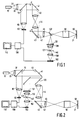
- FIG. 1 shows diagrammatically a first embodiment of the scanning optical microscope according to the invention.
- a radiation source 10 for example, a laser emits a radiation beam 20 which is focussed via a collimator system 30, a pair of beam-deflecting elements 40 an 42, and an objective system 50 to a scanning spot 21 on the surface 60.
- the two beam-deflecting elements are shown in the Figure as flat mirrors which are rotatable about an axis, but alternatively, the beam-deflecting elements may be, for example a rotatable polygon with reflective side faces or an electroacoustic element.
- the axis of rotation 41 of mirror 40 is at right angles to the plane of the drawing and the axis of rotation 43 of the mirror 42 is located in the plane of the drawing.
- an orientation of the mirror 42 and the axis 43 will in practice be chosen in which the radiation path between the mirror 42 and the surface 60 will be directed substantially perpendicularly to the plane of the drawing.
- a lens system 44 To avoid imaging errors and loss of light due to the finite distance between the two mirrors 40 and 42, they are imaged on each other by means of a lens system 44.
- the radiation in the scanning spot 21 which is reflected from the surface 60 is received by the objective system 50 and coupled out to a lens system 80 by a beam splitter 70 via the mirrors 40 and 42. Via this lens system the radiation reaches a radiation detector 90 generating an electrical signal which may be used to form an image of the surface on an image display unit 110, for example a video monitor or a printing-device, by means of the image-processing system 100.
- a radiation detector 90 generating an electrical signal which may be used to form an image of the surface on an image display unit 110, for example a video monitor or a printing-device, by means of the image-processing system 100.
- the beam splitter 70 is arranged between the collimator lens 30 and the mirror 40, but other positions, for example between the objective system 50 and the mirror 42 are alternatively possible, provided that the displacement of the radiation beam in the beam splitter due to scanning of the surface is taken into account.
- the image formed on the image display unit 110 is an accurate linear image of the surface 60
- information about the position of the scanning spot 21 on the surface 60 must be available in the image-processing system 100.
- this information originates from a reference plane 140 on which a sub-beam split off from the radiation beam 20 by a beam splitter 120 is focussed to a reference spot by means of a lens system 130.
- the information about the position may originate directly from the reference plane, for example, because a position-dependent radiation-sensitive detection system is arranged in this plane.
- a greater accuracy is, however, achieved by arranging a grating 140 with a constant grating period in the reference plane and by arranging a radiation-sensitive detection system 160 behind the grating.
- the reference spot is displaced on the grating 140 the reference beam is modulated and thus a corresponding modulation is produced in the output signal of the detection system 160.
- One period in the output signal then corresponds to a fixed distance on the surface 60 of the object, provided that there are no distortions in the two branches whereby a linear image is disturbed.
- a cylindrical lens 131 is arranged in the radiation path of the reference beam.
- the cylindrical lens extends the scanning spot to an elongated spot whose longitudinal direction is parallel to the direction of the grating lines of the grating. The sensitivity of the reference system to dust and dirt on the grating is reduced thereby.
- Figure 2 shows a slightly different embodiment of the scanning optical microscope according to the invention.
- the comparable details in the drawing are denoted by the same reference numerals as in Figure 1 and consequently they do not need any further explanation.
- the beam splitter 120 is arranged in the direction path between the two beam-deflecting elements 40 and 42. Consequently the clock signal, which is generated in the reference branch, is not subject to interferences and signal loss due to the beam-deflecting element 42.
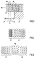
- FIGS 3, 4 and 5 show diagrammatically three embodiments of gratings which can be used in the reference plane. Each of these embodiments not only comprise the actual grating but also an area which serves to indicate a reference or starting point in the signal modulated by means of the grating.
- the actual grating 300 comprises a plurality of juxtaposed light and dark strips 302 and 303, respectively.
- the dark strips 303 are, for example, radiation-absorbing and the light strips are radiation-transparent or radiation-reflective.
- the shape of a reference spot 310 formed on the grating is denoted by a broken line.
- the spot 310 is displaced on the grating in the direction indicated by the arrow 311.
- the radiation from the reference beam passed or reflected by the grating is then periodically modulated in conformity with the displacement of the reference spot.
- the modulation and hence the displacement of the reference spot on the grating is detected by a radiation detector which is arranged in the radiation path of the modulated reference beam.
- the grating period is preferably between a quarter and half the width of the radiation spot so that a uniform wave-shaped modulation is brought about.
- Two areas 320 and 321 are arranged next to the grating 300, which areas have mutually different optical properties and in which the bounding line 322 between these areas extend parallel to the direction of the grating lines.
- the optical properties of the areas are, for example, such that area 320 is comparable with the light strips 302 in the grating 300 and that area 321 is comparable with the dark strips 303.
- the grating shown in Figure 3 requires two radiation detectors, one for detecting the clock pulse signal and one for detecting the bounding line 322 between the areas 320 and 321. Each of the two detectors should be provided with supply and read circuits and they should be aligned with respect to each other.
- Figure 4 shows a grating with which the position of the starting point can be determined more accurately by means of one detector only. Here again the starting point is indicated by the bounding line between two areas having different optical properties, the bounding line being at right angles to the direction of movement of the reference spot.
- the one area denoted by 400 is the grating itself, the other area 420 is an adjoining grating area which is in alignment with the grating 400. This other area 420 has a transmission or reflection coefficient for radiation which is approximately equal to the average value of that of the grating 400.
- this is realized by giving the area 420 the structure of a grating whose grating lines are parallel to the direction of the grating lines in the actual grating 400, but in which the grating period is considerably smaller than the width of the reference spot.
- Figure 5 shows another embodiment for providing a starting point in a grating.
- the grating period of the area 520 is approximately equal to the grating period of the actual grating.
- the direction of the grating lines is, however, parallel to the direction of displacement of the reference spot.
- the area 520 with optical properties different from the grating is arranged within the grating between two grating parts 501 and 502. Otherwise this grating is comparable with the grating shown in Figure 4.
Landscapes
- Physics & Mathematics (AREA)
- Chemical & Material Sciences (AREA)
- Analytical Chemistry (AREA)
- General Physics & Mathematics (AREA)
- Optics & Photonics (AREA)
- Microscoopes, Condenser (AREA)
Claims (8)
- Microscope optique à balayage comportant une unité de source de rayonnement (10) pour fournir un faisceau de rayonnement, un système d'objectif (50) pour focaliser le faisceau de rayonnement de manière à former un spot de balayage (21) sur un plan d'objet (60), un élément de déviation de faisceau (40, 42) disposé dans le trajet de rayonnement du faisceau de rayonnement pour déplacer ledit spot de balayage sur ledit plan d'objet, un diviseur de faisceau (120) pour séparer un faisceau de référence dudit faisceau de rayonnement, un système de détection (160) sensible au rayonnement comportant un plan de référence (140) disposé dans le trajet de rayonnement dudit faisceau de référence pour détecter la position d'un spot de référence (121) formé par ledit faisceau de référence sur ledit plan de référence, ainsi qu'un réseau (300) situé sur ledit plan de référence, caractérisé en ce que ledit diviseur de faisceau est disposé dans le trajet de rayonnement du faisceau de rayonnement entre ledit élément de déviation de faisceau et ledit système d'objectif, en ce que ledit réseau (300) présente des lignes de réseau (302, 303) s'étendant dans une direction sensiblement transversale à la direction de déplacement dudit spot de référence déterminé par ledit élément de déviation de faisceau et en ce qu'une lentille cylindrique (131) est disposée dans le trajet de rayonnement dudit faisceau de référence pour déformer ledit spot de référence de manière à former une ligne de référence s'étendant dans une direction sensiblement transversale à ladite direction de déplacement.
- Microscope selon la revendication 1, caractérisé en ce que le microscope comporte un deuxième élément de déviation de faisceau (42) pour déplacer ledit spot de balayage (21) sur le plan d'objet dans une direction sensiblement perpendiculaire à ladite direction de déplacement déterminée par le premier élément de déviation de faisceau et en ce que ledit diviseur de faisceau (120) est disposé dans le trajet de rayonnement du faisceau de rayonnement entre lesdits premier et deuxième éléments de déviation de faisceau.
- Microscope selon la revendication 1 ou 2, caractérisé en ce que le réseau (300) présente une période de réseau dont la largeur est comprise approximativement entre un quart de la largeur et approximativement la largeur entière dudit spot de référence (121) dans la direction de déplacement déterminée par le premier élément de déviation de faisceau.
- Microscope selon la revendication 1, 2 ou 3, caractérisé en ce que ledit réseau (300) est muni d'une indication de point de départ (322) qui peut être détectée par l'intermédiaire dudit spot de référence.
- Microscope selon la revendication 4, caractérisé en ce que ladite indication de point de départ (322) est constituée par une ligne de séparation (322) s'étendant parallèlement auxdites lignes de réseau (302, 303) entre deux zones (320, 321) sur ledit plan de référence, les propriétés optiques desdites deux zones étant mutuellement différentes.
- Microscope selon la revendication 5, caractérisé en ce que lesdites zones (320, 321) sont situées à côté dudit réseau (300).
- Microscope selon la revendication 5, caractérisé en ce que l'une desdites deux zones (400) est constituée par ledit réseau (400) et en ce que l'autre (420) est une zone dont le coefficient de transmission ou de réflexion pour le faisceau de référence est sensiblement constant, ledit coefficient de transmission ou de réflexion étant sensiblement égal au coefficient de transmission ou de réflexion moyen dudit réseau (300).
- Microscope selon la revendication 7, caractérisé en ce que ladite zone (420) ayant un coefficient de transmission ou de réflexion sensiblement constant est constituée d'un réseau présentant une constante de réseau inférieure à un quart de la taille dudit spot de référence (121).
Applications Claiming Priority (2)
| Application Number | Priority Date | Filing Date | Title |
|---|---|---|---|
| NL8701716 | 1987-07-21 | ||
| NL8701716A NL8701716A (nl) | 1987-07-21 | 1987-07-21 | Aftastende optische mikroskoop. |
Publications (2)
| Publication Number | Publication Date |
|---|---|
| EP0300571A1 EP0300571A1 (fr) | 1989-01-25 |
| EP0300571B1 true EP0300571B1 (fr) | 1993-03-31 |
Family
ID=19850349
Family Applications (1)
| Application Number | Title | Priority Date | Filing Date |
|---|---|---|---|
| EP88201517A Expired - Lifetime EP0300571B1 (fr) | 1987-07-21 | 1988-07-14 | Microscope optique à balayage |
Country Status (5)
| Country | Link |
|---|---|
| US (1) | US4861982A (fr) |
| EP (1) | EP0300571B1 (fr) |
| JP (1) | JPS6437521A (fr) |
| DE (1) | DE3879790T2 (fr) |
| NL (1) | NL8701716A (fr) |
Cited By (5)
| Publication number | Priority date | Publication date | Assignee | Title |
|---|---|---|---|---|
| US7794839B2 (en) | 2003-08-06 | 2010-09-14 | The Procter & Gamble Company | Coated water-swellable material comprising hydrogel forming polymers |
| US7847144B2 (en) | 2003-09-25 | 2010-12-07 | The Procter & Gamble Company | Absorbent articles comprising fluid acquisition zones with superabsorbent polymers |
| US7947865B2 (en) | 2003-08-06 | 2011-05-24 | The Procter & Gamble Company | Absorbent structure comprising water-swellable material |
| US8137746B2 (en) | 2003-08-06 | 2012-03-20 | The Procter & Gamble Company | Process for making water-swellable material comprising coated water-swellable polymers |
| US8287999B2 (en) | 2005-02-04 | 2012-10-16 | The Procter & Gamble Company | Absorbent structure with improved water-absorbing material comprising polyurethane, coalescing aid and antioxidant |
Families Citing this family (21)
| Publication number | Priority date | Publication date | Assignee | Title |
|---|---|---|---|---|
| GB8817672D0 (en) * | 1988-07-25 | 1988-09-01 | Sira Ltd | Optical apparatus |
| US5057686A (en) * | 1988-10-12 | 1991-10-15 | Mitutoyo Corporation | Self-stabilizing photoelectric displacement detector |
| JP3018687B2 (ja) * | 1991-12-12 | 2000-03-13 | 松下電器産業株式会社 | 走査型レーザー顕微鏡 |
| JPH06148525A (ja) * | 1992-10-30 | 1994-05-27 | Koike Seiki Kk | 共焦点レーザー顕微鏡 |
| US5594242A (en) * | 1993-09-09 | 1997-01-14 | Kabushiki Kaisha Topcon | Position detecting apparatus which uses a continuously moving light spot |
| US5880880A (en) * | 1995-01-13 | 1999-03-09 | The General Hospital Corp. | Three-dimensional scanning confocal laser microscope |
| US6108127A (en) * | 1997-05-15 | 2000-08-22 | 3M Innovative Properties Company | High resolution confocal microscope |
| DE59915024D1 (de) * | 1998-02-20 | 2009-06-25 | Leica Microsystems | Anordnung zum kalibrieren eines laserscanmikroskops |
| DE19944148C2 (de) * | 1999-09-15 | 2003-08-21 | Leica Microsystems | Mikroskop |
| US6423960B1 (en) * | 1999-12-31 | 2002-07-23 | Leica Microsystems Heidelberg Gmbh | Method and system for processing scan-data from a confocal microscope |
| DE10160172B4 (de) * | 2001-12-07 | 2016-06-09 | Carl Zeiss Microscopy Gmbh | Laserscanningmikroskop und Laserscanningmikroskopieverfahren |
| US7129473B2 (en) * | 2003-05-16 | 2006-10-31 | Olympus Corporation | Optical image pickup apparatus for imaging living body tissue |
| US20080154224A1 (en) * | 2005-02-04 | 2008-06-26 | Basf Aktiengesellschaft | Process for Producing a Water-Absorbing Material Having a Coating of Elastic Filmforming Polymers |
| TW200635959A (en) * | 2005-02-04 | 2006-10-16 | Basf Ag | Water swellable material |
| DE602006015422D1 (de) * | 2005-02-04 | 2010-08-26 | Basf Se | Verfahren zur herstellung eines wasserabsorbierenden materials mit einem überzug aus elastischen filmbildenden polymeren |
| EP1846049B1 (fr) * | 2005-02-04 | 2011-08-03 | Basf Se | Materiau absorbant l'eau avec revetement de polymeres formant un film elastique |
| JP4877634B2 (ja) * | 2008-10-09 | 2012-02-15 | 修 永井 | ナースコールクリップ |
| JP6084227B2 (ja) * | 2011-10-20 | 2017-02-22 | エーエスエムエル ネザーランズ ビー.ブイ. | リソグラフィ装置及び方法 |
| JP5896797B2 (ja) * | 2012-03-16 | 2016-03-30 | オリンパス株式会社 | ピクセルクロック発生装置 |
| EP3538941A4 (fr) | 2016-11-10 | 2020-06-17 | The Trustees of Columbia University in the City of New York | Procédés d'imagerie rapide de grands échantillons à haute résolution |
| CN106990542B (zh) * | 2017-05-26 | 2023-07-04 | 四川瑞丰锻造有限公司 | 稳定性好的分光器 |
Family Cites Families (8)
| Publication number | Priority date | Publication date | Assignee | Title |
|---|---|---|---|---|
| US3849004A (en) * | 1973-10-11 | 1974-11-19 | Geisco Ass | Photo-detector for optical inspection system |
| US4037941A (en) * | 1975-06-30 | 1977-07-26 | International Business Machines Corporation | Inspection tool |
| US4152588A (en) * | 1977-10-28 | 1979-05-01 | Hughes Aircraft Company | Infrared scanning and display system having a noncontacting angle encoder |
| JPS5850333U (ja) * | 1981-09-30 | 1983-04-05 | スズキ株式会社 | 車輛用油圧式クツシヨン装置 |
| JPS6197619A (ja) * | 1984-10-19 | 1986-05-16 | Fuji Photo Film Co Ltd | 光学式リニアエンコ−ダ |
| US4643569A (en) * | 1985-06-18 | 1987-02-17 | Lincoln Laser Company | Dual beam laser inspection apparatus |
| DE3531129A1 (de) * | 1985-08-30 | 1987-03-12 | Siemens Ag | Verfahren und anordnung zum betrieb eines rastermikroskopes |
| US4775788A (en) * | 1986-10-03 | 1988-10-04 | Greyhawk Systems, Inc. | Apparatus for detecting position of a rotating element using a two-grating moire pattern |
-
1987
- 1987-07-21 NL NL8701716A patent/NL8701716A/nl not_active Application Discontinuation
-
1988
- 1988-07-14 EP EP88201517A patent/EP0300571B1/fr not_active Expired - Lifetime
- 1988-07-14 DE DE8888201517T patent/DE3879790T2/de not_active Expired - Fee Related
- 1988-07-15 US US07/219,516 patent/US4861982A/en not_active Expired - Fee Related
- 1988-07-18 JP JP63177254A patent/JPS6437521A/ja active Pending
Cited By (5)
| Publication number | Priority date | Publication date | Assignee | Title |
|---|---|---|---|---|
| US7794839B2 (en) | 2003-08-06 | 2010-09-14 | The Procter & Gamble Company | Coated water-swellable material comprising hydrogel forming polymers |
| US7947865B2 (en) | 2003-08-06 | 2011-05-24 | The Procter & Gamble Company | Absorbent structure comprising water-swellable material |
| US8137746B2 (en) | 2003-08-06 | 2012-03-20 | The Procter & Gamble Company | Process for making water-swellable material comprising coated water-swellable polymers |
| US7847144B2 (en) | 2003-09-25 | 2010-12-07 | The Procter & Gamble Company | Absorbent articles comprising fluid acquisition zones with superabsorbent polymers |
| US8287999B2 (en) | 2005-02-04 | 2012-10-16 | The Procter & Gamble Company | Absorbent structure with improved water-absorbing material comprising polyurethane, coalescing aid and antioxidant |
Also Published As
| Publication number | Publication date |
|---|---|
| NL8701716A (nl) | 1989-02-16 |
| DE3879790T2 (de) | 1993-09-23 |
| EP0300571A1 (fr) | 1989-01-25 |
| US4861982A (en) | 1989-08-29 |
| DE3879790D1 (de) | 1993-05-06 |
| JPS6437521A (en) | 1989-02-08 |
Similar Documents
| Publication | Publication Date | Title |
|---|---|---|
| EP0300571B1 (fr) | Microscope optique à balayage | |
| US4906922A (en) | Voltage mapping device having fast time resolution | |
| EP0176358B1 (fr) | Dispositif de formation d'image | |
| US3866038A (en) | Apparatus for measuring surface flatness | |
| EP0274155B1 (fr) | Microscope | |
| US5006721A (en) | Lidar scanning system | |
| US4798437A (en) | Method and apparatus for processing analog optical wave signals | |
| US20040129858A1 (en) | Automatic focussing device for an optical appliance | |
| US6741082B2 (en) | Distance information obtaining apparatus and distance information obtaining method | |
| US5288987A (en) | Autofocusing arrangement for a stereomicroscope which permits automatic focusing on objects on which reflections occur | |
| AU5190599A (en) | Imaging a three-dimensional structure by confocal focussing an array of light beams | |
| CN106052585B (zh) | 一种面形检测装置与检测方法 | |
| JP2000275027A (ja) | スリット共焦点顕微鏡とそれを用いた表面形状計測装置 | |
| EP0351011B1 (fr) | Dispositif de balayage optique | |
| US4711576A (en) | Wave front aberration measuring apparatus | |
| EP0872722A1 (fr) | Appareil de mesure de particules et méthode pour sa calibration | |
| US5298727A (en) | Device for reading bar codes on semiconductor surfaces | |
| US3418477A (en) | Apparatus for determining the focal point of a light beam | |
| US4054388A (en) | Optical control means | |
| US5170217A (en) | Object measuring apparatus using lightwave interference | |
| US5170221A (en) | Parallel light ray measuring apparatus | |
| EP0310231B1 (fr) | Appareil de mesure optique | |
| JP2950004B2 (ja) | 共焦点レーザ顕微鏡 | |
| US4758731A (en) | Method and arrangement for aligning, examining and/or measuring two-dimensional objects | |
| US6750436B2 (en) | Focus error detection apparatus and method having dual focus error detection path |
Legal Events
| Date | Code | Title | Description |
|---|---|---|---|
| PUAI | Public reference made under article 153(3) epc to a published international application that has entered the european phase |
Free format text: ORIGINAL CODE: 0009012 |
|
| AK | Designated contracting states |
Kind code of ref document: A1 Designated state(s): DE FR GB |
|
| 17P | Request for examination filed |
Effective date: 19890715 |
|
| 17Q | First examination report despatched |
Effective date: 19911029 |
|
| GRAA | (expected) grant |
Free format text: ORIGINAL CODE: 0009210 |
|
| AK | Designated contracting states |
Kind code of ref document: B1 Designated state(s): DE FR GB |
|
| REF | Corresponds to: |
Ref document number: 3879790 Country of ref document: DE Date of ref document: 19930506 |
|
| ET | Fr: translation filed | ||
| PLBE | No opposition filed within time limit |
Free format text: ORIGINAL CODE: 0009261 |
|
| STAA | Information on the status of an ep patent application or granted ep patent |
Free format text: STATUS: NO OPPOSITION FILED WITHIN TIME LIMIT |
|
| 26N | No opposition filed | ||
| REG | Reference to a national code |
Ref country code: FR Ref legal event code: CD |
|
| PGFP | Annual fee paid to national office [announced via postgrant information from national office to epo] |
Ref country code: DE Payment date: 19960924 Year of fee payment: 9 |
|
| PGFP | Annual fee paid to national office [announced via postgrant information from national office to epo] |
Ref country code: GB Payment date: 19970701 Year of fee payment: 10 |
|
| PGFP | Annual fee paid to national office [announced via postgrant information from national office to epo] |
Ref country code: FR Payment date: 19970722 Year of fee payment: 10 |
|
| PG25 | Lapsed in a contracting state [announced via postgrant information from national office to epo] |
Ref country code: DE Free format text: LAPSE BECAUSE OF NON-PAYMENT OF DUE FEES Effective date: 19980401 |
|
| PG25 | Lapsed in a contracting state [announced via postgrant information from national office to epo] |
Ref country code: GB Free format text: LAPSE BECAUSE OF NON-PAYMENT OF DUE FEES Effective date: 19980714 |
|
| REG | Reference to a national code |
Ref country code: FR Ref legal event code: CD |
|
| GBPC | Gb: european patent ceased through non-payment of renewal fee |
Effective date: 19980714 |
|
| PG25 | Lapsed in a contracting state [announced via postgrant information from national office to epo] |
Ref country code: FR Free format text: LAPSE BECAUSE OF NON-PAYMENT OF DUE FEES Effective date: 19990331 |
|
| REG | Reference to a national code |
Ref country code: FR Ref legal event code: ST |